ICTON 2011
We.C5.6
Clock Recovery of an Injection-Locked Resonant Tunneling Diode Microwave-Photonics Oscillator 1
B. Romeira1, L.M. Pessoa2, H.M. Salgado2, S. Silva2 and J. M. L. Figueiredo1 Departamento de Física, Optoelectrónica e Telecomunicações, Universidade do Algarve, Portugal 2 INESC Porto, Faculdade de Engenharia, Universidade do Porto, Portugal email:
[email protected], {lpessoa, hsalgado, ssilva}@inescporto.pt,
[email protected]
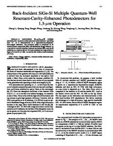
ABSTRACT We show experimental results of clock recovery from return-to-zero (RZ) format data by using injection locking of a free-running optoelectronic oscillator (OEO) circuit, which consists of a resonant tunneling diode (RTD) oscillator integrated circuit with both a detector and optical source. Error free extraction of a clock signal from the RTD-OEO is shown under both optical and electrical injection. The clock recovery performance at ~1.25 Gb/s is analyzed in terms of timing jitter, phase noise and locking bandwidth. Keywords: Clock recovery, injection-locked oscillators, laser diode, microwave photonics, resonant tunnelling diode, timing jitter. 1. INTRODUCTION The ability to recover the clock signal from incoming random data is a fundamental operation in digital communications. Clock recovery consists in deriving a clock signal from the received signal which is synchronized in both frequency and phase, avoiding its transmission along with the data, and providing a timing basis to sample the received signal. In this context, the ability to perform clock recovery using both electrical and optical techniques is an important issue in the development of circuits for novel high-speed optical communication systems. OEOs are a major candidate for that purpose, combining both electronic and photonic components to achieve highly pure microwave signals. OEOs may combine the functions of microwave oscillation and photo-detection, while offering intrinsic gain and high responsivities, being suitable to be injection locked with incoming data in both optical and electrical domains [1]. The RTD-OEO analyzed here, relies on a monolithic integration of a double barrier quantum well (DBQW) with a waveguide photo-detector (PD) at 1.55 µm which works as a RTD-PD oscillator that subsequently drives a laser diode. The RTD-based oscillator takes advantage of the RTD-PD highly nonlinear current-voltage (I-V) characteristic with a wide bandwidth negative differential resistance (NDR) region that can be used to produce self-sustained oscillations at very high frequencies. In fact, RTDs can self-oscillate with a fundamental frequency above 1 THz, at room temperature [2]. When optically or electrically injection locked, RTD-based oscillators synchronize the frequency and phase of the free-running signal to the external signal, therefore being very attractive in both microwave photonics and optical transmission systems. Recently, we demonstrated electrical injection and electrical-to-optical (E-O) conversion using an optoelectronic voltage controlled oscillator (VCO) at GHz frequencies consisting of an RTD oscillator hybrid integrated with a laser diode, the RTD-LD [3]. This novel concept allows the RTD to synchronize to the phase modulation of the injected wireless signal, therefore modulating the laser with the synchronized radio frequency (RF) subcarrier. The advantage of this concept relies in the integration of both microwave and optical functions in a single chip, which brings not only cost reduction but also increased speed and reliability. Furthermore, optical injection and optical-to-electrical (O-E) conversion was also demonstrated using a unipolar semiconductor optical waveguide photo-detector incorporating an RTD, the RTD-PD [4]. Additionally, the RTD-PD was integrated with a LD, the RTD-PD-LD, having both optical and electrical input and output ports, Fig. 1(a). This device does not require additional techniques to produce stable low-phase noise signals, allowing the realization of simple and compact low phase-noise microwave-photonic oscillators for optical-electrical signal processing and for Radio-over-Fiber (RoF) cellular network base stations [5].
Figure 1: (a) RTD-PD monolithic integrated chip and laser diode chip (not scaled) showing optical and electrical input and output ports; (b) I-V characteristic of the RTD-PD device in series with the LD and frequency tuning curve of RTD-OEO free-running oscillations; (c) Schematic of RTD-OEO electrical and optical injection and output ports.
978-1-4577-0882-4/11/$26.00 ©2011 IEEE
1
ICTON 2011
We.C5.6
Here we demonstrate clock recovery from return-to-zero (RZ) format data by using injection locking of a freerunning OEO circuit. The performance of both optically and electrically recovered clocks was assessed considering the following parameters: timing jitter, phase noise and locking bandwidth. Additionally, bit-errorrate (BER) measurements were carried out using the recovered clock as a timing base for the sampling of the received data. 2. RTD-OEO DESCRIPTION AND EXPERIMENTAL SETUP The experimental demonstration of clock recovery was performed using an OEO circuit consisting of a RTDPD, which provides O-E conversion, hybrid integrated with a laser diode, for E-O conversion, Fig. 1(a). The measured responsivity of the O-E conversion is ~0.3 A/W while the E-O conversion efficiency is ~0.25 W/A. The ridge waveguide structure gives an advantage to traditional RTD-PDs by providing light confinement along the DBQW plane [6]. The LD is a 5 μm ridge waveguide designed for continuous-wave emission at around 1.55 µm with a threshold current of ∼ 6 mA. When biased in the NDR region, self-sustained current oscillations builds-up and modulate the LD, incorporating into the circuit optical output an RF sub-carrier that mimics the current self-oscillations. The circuit I-V characteristic is shown in Fig. 1(b), where it is indicated that the natural oscillation frequency is bounded between 0.98 GHz and 1.25 GHz, within the NDR region. In the experimental setup, bias settings for 1.25 GHz and 1.24 GHz were considered for the electrical and optical injection setups, respectively, close to the valley region of the NDR where higher responsivity is also obtained [4]. Figure 1(c) shows the RTD-OEO injection locked schematic setup. As depicted, the incoming data can be injected into the OEO either optically or electrically. The free running OEO is tuned to oscillate at a frequency sufficiently close to the incoming signal. The locking range is typically on the order of kHz up to MHz, depending on the power of the injected clock frequency. With the injection of the incoming signal, the RTDOEO locks to the clock frequency in a time inversely proportional to the locking range. The recovered signal can be accessed both at the optical and electrical output ports. In the following sections, we present and discuss the electrical and optical injection locking results showing stable frequency and low-jitter noise signals and demonstrate clock recovery and error free timing extraction of 1.25 Gb/s and 1.24 Gb/s data streams. 3. E-O INJECTION LOCKING 3.1 Experimental Setup The electrical injection setup consisting of an electrical input and optical output signals is shown schematically in Fig. 2. The RTD-OEO was DC biased for a free-running oscillation frequency of approximately 1.25 GHz. Then an electrical input signal was injected, consisting of a RZ pseudorandom bit stream (PRBS) at 1.25 Gb/s generated from a BER transmitter, whose spectrum is shown in Fig. 3(a), and respective eye diagram in Fig. 3(b). Two different amplitude levels were tested for the RZ data stream, specifically 100 mV and 500 mV. The recovered clock was accessed at the laser optical output and then converted to the electrical domain using a commercial photo-diode.
(a)
20.5 mV/div
(b)
200 ps/div
Figure 2. RTD-OEO experimental schematic for timing extraction.
Figure 3. RZ data stream input of 1.25 Gb/s using a PRBS of 27-1 using a clock signal with 100 mV amplitude (Vp-p) and 50% duty cycle: (a) RZ data stream measured in the frequency domain, b) Eye diagram of RZ data.
3.2 Measurement results Figure 4 shows the electrical spectrum of both free-running oscillation and the injection locked RTD-OEO photo-detected optical output. The RTD-OEO output oscillation frequency was clearly pulled to 1.25 GHz with a significant phase noise reduction of more than 30 dB, as shown in Fig. 5. The noise floor of the recovered clock is approximately 10 dB higher than that of the original clock signal. The 1/f noises of the recovered signals are similar to that of the original clock signal. For example, the phase noise of the recovered clock at 10 kHz
2
ICTON 2011
We.C5.6
offset is -103.8 dBc/Hz and almost matches the original clock of -104.5 dBc/Hz. The locking range was verified to depend on the power of the injected signal, varying from 1 MHz up to 9.1 MHz, for the tested range of signal levels. The inset of Fig. 4 shows the temporal waveform of the recovered clock. To perform this measurement, the oscilloscope was triggered by the original clock signal. Additionally, the oscilloscope indicated a root-meansquare (rms) jitter of 6.26 ps, which matches well with that from the phase noise measurement. The integrated timing jitter over a 90-kHz bandwidth was < 4 ps and compares with the timing jitter measured by the oscilloscope. 12.6 mV/div
200 ps/div
Figure 4. The 1.25 Gb/s recovered clock LD photo-detected signal from an RZ data stream (100 mV amplitude) measured in the frequency domain. The inset is shows the LD output recovered clock in the time domain.
Figure 5. SSB phase noise of free-running, recovered clock signals (at 100 mV and 500 mV) and injected RZ signal (at 500 mV).
4. O-E INJECTION LOCKING
Voltage (mV)
4.1 Experimental Setup Figure 6 shows the experimental schematic for timing extraction and BER measurements. A 1.24 Gb/s RZ signal was used to modulate a tunable laser diode optical carrier at 1550 nm using a 10 Gb/s modulator that then fed an EDFA which output was subsequently split in a 50/50 coupler. One of the coupler outputs went to a commercial photo-receiver whose output was connected to the error analyzer. The other part of the optical signal was coupled to the RTD-PD waveguide. 14.2 mV/div
200 ps/div
Time (ps)
Figure 6. RTD-OEO experimental schematic for timing extraction and BER measurements.
Figure 7. Power spectrum of the 1.24 GHz clock signal recovered from an optical-modulated RZ data stream (500 mV amplitude). The optical injection power was ~4.84 dBm.
4.2 Measurement results Figure 7 shows the spectra traces of the free-running oscillation slightly above 1.24 GHz and the injection locked output at 1.24 GHz. The inset of Fig. 7 presents the injection locked RTD-OEO time domain output signal, for an optical injection power of 0.52 dBm. The output spectrum was clearly pulled to 1.24 GHz in the presence of the optical injected signal. The phase noise was considerably reduced as shown in Fig. 8. A phase noise reduction of ~24 dB at 10 kHz offset from the carrier frequency is achieved for an optical injection power in the fiber of around 7.85 dBm. The minimum optical power in the fiber to obtain locking was around 0.52 dBm with a locking range of 0.3 MHz. We observed the locking range and the phase noise reduction were strongly dependent on the optical power of the optically modulated injected signal. The rms jitter measured by the
3
ICTON 2011
We.C5.6
oscilloscope was 2.16 ps, which also matches well with that from phase-noise measurement. The integrated timing jitter over a 90-kHz bandwidth was < 2 ps and compares with the timing jitter measured with the oscilloscope. 4.3 Bit-error-rate (BER) measurement A comprehensive way to characterize the performance of a recovered clock signal is to measure the BER. First, the quality of data detection was investigated for a direct clock situation where the clock signal from the pattern generator was used to trigger the bit error rate tester. Next, clock recovery was performed and the optically injection locked RTD electrical output was used to trigger the bit error tester. To reduce the effect of environmental fluctuations, the measurement time was 10 s and the data pattern length was 27 – 1. Fig. 9 shows the BER at 1.24 Gb/s as a function of the received power for both direct and recovered clocks.
Figure 8. SSB phase noise of free-running and recovered clock signals.
Figure 9. BER measurement of RTD-OEO recovered clock and direct clock.
The two BER curves are similar, provided the low jitter of the extracted RTD-OEO clock signal. It is believed that the mismatch in some of the BER points results from environmental instabilities (vibration, temperature fluctuations) which can be reduced significantly with further optimizations in the measurement setup. 5. CONCLUSIONS We have presented experimental results of clock recovery from return-to-zero (RZ) format data by using injection locking of a free-running optoelectronic oscillator circuit. The timing jitter, phase noise, and locking bandwidth aspects of optical- and electrical recovered clocks were investigated. The performance of the recovery clock was also investigated using bit-error-rate (BER) measurements. The RTD-OEO is a simple and compact circuit configuration with interesting applications over a wide range of RF-photonic systems such as distribution of low-phase noise signals, and stable RF carriers in communication links. ACKNOWLEDGMENT This work was supported by FCT under the project WOWi (PTDC/EEA-TEL/100755/2008) and in the framework of programme POCTI/FEDER with grant REEQ/1272/EEI/2005. B. Romeira also acknowledges support from FCT through a PhD grant (SFRH/BD/43433/2008). B. Romeira and J. M. L. Figueiredo acknowledge the fruitful discussions with Professor Charles N. Ironside and Dr. A. E. Kelly of the School of Engineering, University of Glasgow, UK, on RTD optoelectronic oscillators. REFERENCES [1] X. Y. Yao and L. Maleki, “Optoelectronic oscillator for photonic systems,” IEEE J. Quantum Electron., vol. 32, no. 7, 1996. [2] S. Suzuki, et al., “Fundamental oscillation of resonant tunneling diodes above 1 THz at room temperature,” Appl. Phys. Lett., vol. 97, 2010. [3] B. Romeira, et al., “Nonlinear dynamics of resonant tunneling optoelectronic circuits for wireless/optical interfaces,” IEEE J. Quantum Electron., vol. 45, no. 11, pp. 1436-1445, Nov. 2009. [4] B. Romeira, et al., “Optical control of a resonant tunneling diode microwave-photonic oscillator,” IEEE Photon. Technol. Lett., vol. 22, no. 21, pp. 1610-1612, Nov. 1, 2010. [5] A. J. Seeds and K. J. Williams, “Microwave photonics,” J. Lightw. Technol., vol. 24, no. 12, pp. 4628-4641, 2006. [6] T. Ramond, L. Hollberg, P. W. Juodawlkis, and S. D. Calawa, “Low-noise optical injection locking of a resonant tunneling diode to a stable optical frequency comb,” Appl. Phys. Lett., vol. 90, p. 171124, 2007.
4