Infineon Technologies, Villach, Austria. ABSTRACT. In this study consideration is made of the common mode (CM) behavior of two-stage fully differential.
COMMON MODE STABILITY IN FULLY DIFFERENTIAL VOLTAGE FEEDBACK CMOS AMPLIFIERS Arturo Tauro*, Cristoforo Marzocca*, Francesco Corsi*, Antonio Di Giandomenico** * Dipartimento di Elettrotecnica ed Elettronica, Politecnico di Bari, Italy ** Infineon Technologies, Villach, Austria
ABSTRACT In this study consideration is made of the common mode (CM) behavior of two-stage fully differential amplifiers in voltage feedback connection. In particular, interaction between internal CMFB circuitry and the external feedback network is investigated in order to highlight a possible operating point instability condition, due to the presence of a positive feedback loop. Two alternative CMFB topologies are compared, one of which is affected by instability, with development of constraints on the feedback network parameters to be fulfilled in order to avoid instability. Comparison was made by circuit simulations with reference to a low voltage, deep sub-micron CMOS technology (0.12 µm) implementation of a differential amplifier.
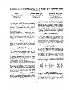
may cause the set up of an erroneous d.c. operating point at the amplifier power on. Fig.1 shows the schematic of a differential voltage amplifier implemented with a fully differential Opamp. One of the feedback loops, internal to the Opamp, includes the CMFB circuitry, while the other is made up of the external passive feedback network and the CM signal path of the Opamp. While the former achieves negative feedback, the latter is positive for a typical two-stage amplifier, and may cause instability. R2 1
R1
3
+ -
5
2
R1
4
- +
6
Vout=V’in
V’in
R2
Figure 1 – Fully-Differential voltage feedback Opamp.
1. INTRODUCTION Fully differential circuit structures are at present widely employed in low voltage (LV) applications, due to their improved immunity to noise, larger output swings and reduced distortion. However, these benefits are obtained at the expense of greater complexity, since differential amplifiers usually require internal common mode feedback (CMFB) loop in order to stabilize their d.c. voltages at both internal and output nodes. Although a great amount of work is currently underway which addresses this problem either by optimizing the CMFB loop in terms of linearity, speed, power consumption, and so on [1,2], or by trying to control the CM without employing any additional circuitry [3,4], no general solution is presently available since the variety of different situations arising in practical applications requires special approaches. This study shows that two distinct CMFB loops are generally active in a differential voltage amplifier with internal CMFB circuitry [5] and identify the conditions for which their interaction
In order to distinguish between the two loops, the former is referred to as ‘internal’, while the latter is ‘external’. According to this definition, Tint and Tex represent corresponding loop gains while V’icm, Vicm and Vocm are CM voltages at nodes 1-2, 3-4 and 5-6 respectively, as indicated in Fig.1. 2. ANALYZING THE CMFB LOOP The problem can be studied in its essential aspects with reference to simple Miller Opamp architecture, although analysis can easily be extended to more complex situations including both telescopic and folded cascode topologies, circuits or opamps. An initial CMFB topology is analyzed here which sets up CM control by regulating gate voltage across M0, as shown in Fig.2. In this figure, ACMFB, which is negative, represents the voltage gain of the CMFB circuit, while M0 is in the saturation region. Apparently, the amplifier has a non-inverting common-mode gain, Acm, resulting as it does from cascade connection of two inverting stages. As a consequence, as has already been pointed out, a positive feedback effect arises when the external
0-7803-8163-7/03/$17.00 © 2003 IEEE
ICECS-2003
288
differential feedback network is connected which may affect overall amplifier stability. In fact,
Vr2
M7
M0/2
A
R1 , the denoting the feedback factor by: f = R1 + R 2
external CM loop gain, Tex = Acm·f, must be kept smaller than unity so as to avoid instability.
C MFB
VoCM M1
ViCM
M3 M0
A Vr2
VoCM
M5
C MFB
M7
M8
Vin-
M1
M2
Vin+
Vout-
Figure 3 – CM Half circuit of the amplifier.
Vout+ M3
Vr1
M4
Vr1
M5
R R Vocm = 1 + 2 Vicm − 2 ⋅ VREF R1 R1
M6
Figure 2 – Miller Opamp employing a CMFB topology regulating the gate voltage across M0.
In particular: A cm =
A cm0 , where: Acm0 is the CM 1 + Tint
gain without the CMFB circuit and Tint is the internal CM loop gain. Defining the impedances at the drain of the cascode and output transistors by rp1 and rp2 respectively, Tint can be calculated from the CM half circuit of the amplifier shown in Fig.3: Tint = A CMFB
g m0 rp1g m3 rp2 2
(1)
As Acm0 has a low value due to the high CMRR of the Opamp, Acm will normally be very small. However, with reference to the CM loop in Fig.2, an increase of the CM signal Vicm, at the input of the amplifier, may lead the transistor M0 to operate in its triode region, in which case the circuit assumes a nonlinear behavior since the M0 output resistance is no longer constant. Reducing output resistance of the tail current source will cause a decrease in CMRR and an increase in Acm0, with Tint also dropping owing to its proportionality to gm0. As a result, Acm increases along with Tex. The amplifier d.c. operating point is determined by the equilibrium condition resulting from the simultaneous action of both internal and external feedback loops. If V’icm = VREF = cost., the expression of the static characteristic of the external feedback network is simply:
(2)
Graphical representation of this relationship, with k= R2 / R1, is shown in Fig.4 (solid lines). The slope of these characteristics is 1/f. The dashed curve refers to the static input-output CM characteristic of the Opamp. The equilibrium condition must satisfy the constraints imposed by both characteristics and corresponds to the intersection of the two curves of Fig.4. Owing to the non-linearity of Acm, the equilibrium condition may not be univocally identified, also depending on the values assumed by the two resistors R1 and R2. In particular, a range [0, k*] exists, such that three distinct intersection points occur when 0 < k < k*, while a single equilibrium point exists for k > k*. For example, assuming VREF = 0.7 V and VDD = 1.5 V leads to a value of k* = 1.67 (obtained by setting Vocm = VDD and Vicm = VDD-VSG-VSDsat in eq. (2)). Thus even a simple, widely employed, voltage buffer (k = 1) may be affected by the described operating point ambiguity. Analysis of Fig.4 appears to indicate that for k within the interval [0, k*], points 1 and 3 correspond to stable equilibrium conditions, since they refer to low values of Acm, while point 2 is unstable, since it occurs in correspondence with a high Acm value. This is also apparent from evaluation of the slope of the dashed line at point 2. Under these conditions, in fact, Acm> 1/f or, equivalently, Tex > 1. In order to check for the validity of the above conclusions, circuit simulations were carried out with reference to a low voltage deep sub-micron
289
obtain Vicm = 1.1V which falls outside the CM input dynamic range of the Opamp, corresponding (Fig.5) approximately to the interval [0, 0.9V]. Simulation (Fig.6) confirms that the circuit leaves the operating point 3 for V’icm = 0.3V, obtained by evaluating VREF in eq. (2) for Vicm = 0.9V and Vocm = VDD.
Vocm VDD 3
1
VREF
2
k=0 k=k* 0
VREF
Vicm
Figure 4 – Static input-output CM characteristic of the open loop Opamp (dashed line). Eq. (2) has been plotted (solid lines) for two values of k: k=0 and a generic value k*.
CMOS technology (0.12 µm) implementation of a differential amplifier. Values for VDD and VREF are respectively 1.5V and 0.7 V. A voltage buffer configuration has been chosen: R1 = R2 = R, with CMFB circuit assumed to have a unity gain.
Figure 6 – Transient CM output voltage of the feedback amplifier (solid line) and input signal V’icm (dotted line).
The operating point ambiguity is apparent from analysis of the figure 5, which shows the CM static input-output characteristics of the open loop Opamp.
3. ALTERNATIVE CMFB TOPOLOGY A dissimilar CMFB topology is obtained by controlling the gate voltage across transistors M5M6, rather than the Vgs of M0. Fig.7 shows the CM half circuit of the Miller Opamp of Fig.2 which employs the above CMFB topology. Evaluation of the internal CM loop gain Tint for the circuit in Fig.7 leads to the following expression: Tint = A CMFB g m5 rp1g m3 rp2
Figure 5 – CM static characteristics of the open loop Opamp. The dotted line corresponds to eq. (2) for k = 1.
A graphical estimation of k* from Fig.5, gives a value of 1.92, not too far from that obtained by manual analysis. Figure 6 shows the transient CM output voltage of the feedback amplifier corresponding to an input triangular signal V’icm. The output signal waveform can be derived from the static characteristic in Fig.5, since input signal frequency is small enough to be considered as a static stimulation. For V’icm approximately equal to 1.2 V, the d.c. amplifier output sets to: Vocm = VDD (point 3 in Fig.4). Once in this erroneus operating condition, the circuit is unable to exit even when V’icm settles to VREF. In fact, setting Vocm = VDD in equation (2), we
(3)
In contrast to the previous case, Tint is now independent from gm0, guaranteeing that Acm and, consequently Tex, are within a relatively low value even when high CM input voltage is applied which reduces gm0. The value of ACMFB can be chosen so as to obtain the desired value of Acm, even though it must also satisfy stability constraints referred to the internal CM loop. Reduction of Acm over a wider range of Vicm well above VREF results in the elimination of the instability condition since no multiple intersection points will be allowed in the plots of Fig.4. Circuit simulations were again carried out under the same conditions as in Figs. 5 and 6, but with the adoption of the second CMFB network, with results presented in Fig.8 and Fig.9.
290
Vr2
M7
Vr1
M0/2
VoCM M1
ViCM
M3
M5
A
Figure 8 – CM static characteristics of the open loop Opamp employing the alternative CMFB network. The dotted line corresponds to eq. (2) for k = 1.
C MFB
Figure 7 – CM half circuit of the amplifier employing the alternative CMFB topology.
Fig.8 shows that a single equilibrium point now exists for Vicm = 0.7 V. This result is also confirmed by transient analysis (Fig.9) since, in this case, the circuit does not enter an erroneous operating condition when stimulated with a full amplitude triangular waveform. However, for high values of the input signal, the output CM voltage Vocm drifts from its correct value, due to variation of the CM gain Acm, as is clearly in evidence looking at the slope of the solid line in Fig.8.
Figure 9 – Transient CM output voltage of the feedback amplifier (solid line) and input signal V’icm (dotted line).
5. REFERENCES 4. CONCLUSIONS This study shows that two distinct feedback loops are generally operating in a differential voltage amplifier with internal CMFB circuitry. The conditions under which their interaction does not allow for univocal determination of the d.c. operating point of the circuit have been identified. In particular, we related the presence of instability to the drop of the internal CM gain Tint for certain values of the input CM signal, which, in turn, increases the value of Acm and Tex. When comparison of the two different topologies of CMFB networks was carried out, only one solution was shown to be affected by instability. The validity of this analysis was checked by simulation with reference to deep submicron CMOS technology implementation.
[1] J. F. Duque-Carrillo, “Continuous-Time CommonMode Feedback Networks for Fully-Differential Amplifiers: a Comparative Study,” Circuits and Systems, 1993., ISCAS ’93, 1993 IEEE International Symposium on, vol. 2. pp. 1267-1270, 3-6 May 1993. [2] P. M. VanPeteghem, J. F. Duque-Carrillo, “A General Description of Common-Mode Feedback in Fully-Differential Amplifiers,” Circuits and Systems, 1990., IEEE International Symposium on, vol.. 4. pp. 320–312, 1-3 May 1990. [3] P. D. Walker and M. M. Green, “An Approach to Fully Differential Circuit Design without CommonMode Feedback,” IEEE Trans. Circuits Syst., vol. 43, pp. 752-762, Nov. 1996. [4] G. Nicollini, F. Moretti and M. Conti, “HighFrequency Fully Differential Filter Using Operational Amplifiers Without Common-Mode Feedback,” IEEE J. Solid-State Circuits, vol. 24. pp. 803-813, Jun. 1989. [5] P.J. Hurst, “Determination of Stability Using Return Ratios in Balanced Fully Differential Feedback Circuits,” IEEE Trans. Circuits Syst., vol. 42, pp. 805-817, Dec. 1995.
291