Available online at www.sciencedirect.com
ScienceDirect Materials Today: Proceedings 5 (2018) 9041–9050
www.materialstoday.com/proceedings
NCNN 2017
Conduction Mechanism and Charge Transporting Property of Te90-xSe10Cdx Chalcogenides by AC Conductivity and Dielectric Analysis Arvind Kumar Verma, Pramesh Chandra, Nishant Kumar, Anchal Srivastava and R.K.Shukla* Department of Physics, University of Lucknow, Lucknow,226007, Uttar Pradesh, India.
Abstract The effects of Cd incorporation on the dielectric properties of chalcogenide alloy Te90-xSe10Cdx (x = 0, 10, 15, 20 at. wt. %) have been studied. These are synthesised by melt quenching technique. Frequency dependence of the AC conductivity, dielectric constants (ε′), dielectric losses (ε′′) and dissipation factor in the frequency range 50Hz -5 MHz at room temperature have been reported. Temperature dependent studies in 298 – 473 K at a fixed audio frequency of 10 kHz have also been measured. It is found that AC conductivity, dielectric loss and dissipation factor increase as frequency and temperature increase. Dielectric constant decreases as frequency increases whereas it increases with increasing temperature. Dielectric constant increases while dielectric loss decreases with increasing Cd content in Te-Se matrix. Possible explanations of metal (Cd) induced effects on the conduction mechanism of the Te90Se10 alloy are discussed. © 2017 Elsevier Ltd. All rights reserved. Selection and Peer-review under responsibility of 6th NATIONAL CONFERENCE ON NANOMATERIALS AND NANOTECHNOLOGY (NATCON NAMTECH VI - 2017)
Keywords: Te90-xSe10Cdx (x = 0, 10, 15,20); XRD; FESEM; LCR METER
*Email address:
[email protected]
2214-7853 © 2017 Elsevier Ltd. All rights reserved. Selection and Peer-review under responsibility of 6th NATIONAL CONFERENCE ON NANOMATERIALS AND NANOTECHNOLOGY (NATCON NAMTECH VI - 2017)
9042
1.
Arvind K.Verma et al/ Materials Today: Proceedings 5 (2018) 9041–9050
Introduction
Dielectrics analysis measurement gives information about the two fundamental electrical characteristics of the material as a function of frequency and temperature. These are the capacitive nature which represents the ability of the materials to store electric charge and the conductive nature which represents the ability of the materials to transfer electric charge. These abilities are called dielectric constant and dielectric loss analysis respectively [1]. Undoped chalcogenide materials show low values of electrical conductivity which limits their technological applications and electrical measurements. Certain additives (semiconductors or metals) are used to improve the conductive properties of the chalcogenide alloys [2]. Dielectrics are a class of materials that are poor conductors of electricity, in contrast to materials such as metals that are generally good electrical conductors. The electrical nature of the synthesised chalcogenide alloys can be described by their dielectric properties which influence the distribution of electromagnetic fields and currents in the region occupied by the materials and also determine the characteristics of the pure and doped synthesised materials in electric fields. The dielectric properties determine how rapidly a material will heat in radio-frequency or microwave dielectric heating applications. Because of the properties of the heated materials, it influences the design of the equipment and its operation. Their influence on the electric fields also provides a means for sensing the properties of the materials, which can be correlated with the dielectric properties, by non-destructive electrical measurements [3]. The frequency-dependent electrical conductivity of chalcogenide semiconductors is helpful to understand the conduction mechanism in their alloys. Therefore, it is interesting to study the electrical behaviour of the materials in a field which gives important information about the transport process in localised state in the forbidden gap [4]. AC conductivity and dielectric measurements have been reported for a wide variety of chalcogenide semiconductors in order to understand the mechanisms of conduction processes as well as types of polarisation in the given materials. Chalcogenide alloys are known to be structurally disordered systems and the addition of impurities in the disordered system changes their structure, which leads to changes in conduction mechanism and varies with different impurities [5]. The main problem of the chalcogenide alloys is the presence of localised states in the mobility gap due to the absence of longrange order as well as various inherent defects [6]. It is well-known that the addition of metallic additives to binary chalcogenide system changes their structure and new properties are expected for these alloys. From this point of view, the effect of the addition of Cd metal on the electrical properties of the Te-Se binary system has been studied. We have performed an AC conduction and dielectrics studies in Te90-xSe10Cdx (x = 0, 10, 15, 20 at. wt. %) alloy to analyse the metal-induced effects on the conduction mechanism and electrical transport properties. 2.
Experimental Methods and Results
Chalcogenide alloy Te90-xSe10Cdx (x = 0, 10, 15, 20 at. wt. %) were prepared from 99.999% pure Te, Se and Cd elements by melt quenching technique. The exact amounts of alloying elements were weighed according to their atomic weight percentages using an electronic balance with the least count of a 10-4 gram. These were then placed into ultra-cleaned quartz ampoules (length ≈ 5 cm and internal diameter ≈ 8 mm). The ampoules were evacuated and sealed under a vacuum of 10-3 Torr to avoid reaction of alloying elements with oxygen at a higher temperature. The sealed ampoules were heated in a furnace at the rate of 40 C/min. The temperature was raised up to 10000 C and was maintained for 10 hours. During the heating process, the ampoules were constantly rocked by a ceramic rod to ensure the homogeneity of the alloying materials. The ampoules with molten materials were rapidly quenched into the ice-cooled water to allow glass formation and to avoid crystallisation. The ingots of synthesised materials were taken out from ampoules by breaking them. The obtained melt was ground into powder form to obtain homogeneous alloy. This was then compressed into pellets having a diameter of 13 mm and thickness of about 1-2 mm under a uniform pressure of 5 tons using a hydraulic press machine. The pellets made from Te90-xSe10Cdx (x = 0, 10, 15, 20) alloy were named as S1 (Te90Se10), S2 (Te80Se10Cd10), S3 (Te75Se10Cd15) and S4 (Te70Se10Cd20). Physical dimensions of each pellet were measured with the help of digital screw-gauge (BAKER-Type J02, 7301) having least count 0.01 mm. Each pellet was sandwiched between two circular brass discs in order to ensure good electrical contact. This whole assembly of pellet and discs was placed between the electrodes of the LCR meter. The signal voltage was kept at 1.0 volt. AC electrical conductivity and dielectric measurements were made with Wayne Kerr 6500 P high-speed LCR meter in the frequency range 20 Hz to 5 MHz. In this entire process, all the pellets used were kept uncoated.
Arvind K.Verma et al / Materials Today: Proceedings 5 (2018) 9041–9050
3.
9043
X-Ray Diffraction
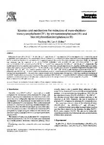
Crystal structure and phases of the samples S1, S2, S3 and S4 of chalcogenide alloy Te90-xSe10Cdx (x = 0, 10, 15, 20 at. wt. %) were determined by X-ray diffraction (XRD) using Ultima IV model from Rigaku, Japan employing Cu Kα radiation (wavelength 1.5404 Å) in the 2θ range from 20° to 80° with a scan speed of 2°/sec. Figure 1 shows the structural peaks diffracted by the crystals of the synthesised samples. The presence of sharp peaks confirms the polycrystalline nature of all the samples. It has been reported by researchers that the XRD pattern of Te-rich alloys shows a high degree of crystallinity [7, 8]. 101
7200 4800 2400
S4(Te70Se10Cd20) 100 002
110 102
201
202
210
0
Intensity
8100
101
S3(Te75Se10Cd15)
5400 2700
100 002
102 110
201
202
210
0 101
8400
S2(Te80Se10Cd10)
5600 2800
102
100 002
110
201
202
210
0 101
6000 4000
S1(Te90Se10)
100
110
2000
102 111
201
202
210
0 20
30
40
50
60
211
70
80
Bragg's angle(2) Fig.1. X-ray pattern of the Te90-xSe10Cdx (x= 0, 10, 15, 20 at.wt. %) alloys
The peaks observed at (1,0,0), (2,0,1), and (2,1,0) confirm the hexagonal phase and the one observed at (101) confirms the cubic phase among all the peaks of the sample S1, S2, S3 and S4 as concluded from DB card no. (000040554).The average crystallite size D corresponding to observed peaks is calculated using Scherrer’s formula (D = Kλ/βcosθ), where k is constant dependent on crystallite shape (=0.89), λ is X-ray wavelength (1.5405Å), β is FWHM (full width at half maxima in radian) and θB is Bragg angle [9, 10, 11]. Using the crystallite size, the rough approximation of a number of defects in the sample is defined by dislocation density (δ) which have been calculated using the formula [12]; δ=n/D2 Where n is a factor, which equals unity giving minimum dislocation density. The crystallite size D and dislocation density (δ) have been calculated using these formulas for all the samples and are given in Table 1. Higher dislocation density in terms of defects is responsible for decreasing the crystal size of the samples [13]. 4.
Surface morphology
In FESEM, the electrons interact with atoms in the sample which produces various signals that can be detected. This gives important information regarding growth mechanism, shape, and size of the samples. Surface morphology of the glassy chalcogenide alloy Te90-xSe10Cdx (x = 0, 10, 15, 20 at. wt. %) was studied using JSM-
9044
Arvind K.Verma et al/ Materials Today: Proceedings 5 (2018) 9041–9050
7610F Model FESEM from JEOL, Japan. Figure 2 shows the Field Emission Scanning Electron Micrographs of the samples S1, S2, S3, and S4 for Te90-xSe10Cdx (x = 0, 10, 15, 20 at. wt. %). It is observed that the surface morphology of the as-prepared bulk samples (pellets) has changed with changing Cadmium content for samples S1, S2, S3, and S4.
Fig.2. FESEM images of the Te90-xSe10Cdx (x= 0, 10, 15, 20 at.wt. %) alloys
From FESEM micrographs, it is evident that the images of the as-prepared sample S1 (undoped) and S2 (10% of Cd) are not in uniform due to defects in the disorder of the nanoparticles which shows irregular and without interconnecting assembly of the particles. Cd-doped sample S3 (15%) an S4(20%) show some pinholes and cracks with a smooth surface as doping concentration increases. Change in crystal size of all samples with increasing Cadmium content is indicated by FESEM images which confirm the correctness of the XRD data. 5. Frequency and Temperature dependent AC conductivity (σac) Measurement of AC conductivity of chalcogenide semiconductors gives information about the conduction process and the nature of charge transport between localised states in the forbidden gap of the materials [14]. The frequency variation studies have been carried out to understand the electrical homogeneity and nature of the electrical conduction in the material. In AC electrical conductivity measurements, the sinusoidal voltage of different frequencies is applied to the sample of thickness d and area A. The AC conductivity is given as σac = 2πfεoε'tanδ, where f is the frequency of the applied signal (50 Hz to 5 MHz), εo is the permittivity of free space, ε'=Cpd/εoA is the real part of dielectric constant and tanδ is loss tangent or dissipation factor [15]. The variation of AC conductivity in the frequency range 50Hz - 5MHz at room temperature and in the temperature range 298–473K at fixed audio frequency of 10 kHz for different compositions of Te90-xSe10Cdx (x = 0, 10, 15, 20 at. wt. %) alloys are shown in Figures 3(a) and (b) respectively. From figure 3(a), it has been observed that AC conductivity increases with increase in frequency.
Arvind K.Verma et al / Materials Today: Proceedings 5 (2018) 9041–9050
1.4x10
14
1.2x10
14
1.0x10
14
8.0x10
13
6.0x10
13
4.0x10
13
2.0x10
13
S1 S2 S3 S4
9
5x10
AC conductivity (ac)
14
AC conductivity ( ac)
1.6x10
9
9045
at 10khz
S1 S2 S3 S4
4x10
9
3x10
9
2x10
9
1x10
3(a)
0.0 4
6
8
10
ln(f) Hz
12
14
16
0
3(b)
300
330
360
390
420
450
480
Temperature(K)
Fig. 3(a).Variation of AC conductivity with ln (f) at room temperature; Fig. 3(b).Variation of AC conductivity for different temperatures at 10 kHz frequency for Te90-xSe10Cdx (x= 0, 10, 15, 20 at. wt. %) alloys.
The graph of σac vs. ln (f) shows the almost frequency-independent region in low-frequency range followed by strong frequency dependence at higher values of frequencies. Enhancement in conduction mechanism is responsible for the increase of AC conductivity in the high-frequency range at room temperature for samples S1, S2, S3 and S4 [16]. Temperature dependence of the AC conductivity (σac) at fixed frequency of 10 kHz was studied for Te90-xSe10Cdx (x = 0, 10, 15, 20 at. wt. %) alloys. Figure 3 (b) shows a plot of σac against different temperatures at 10 kHz frequency for the investigated Cd-doped chalcogenide alloys. It is clear from this figure that σac increases with increasing temperature for the synthesised Cd-doped sample S2 (10%) which has maximum AC conductivity in comparison to the S3(15%), S4(20%) and S1 (undoped) samples. The influence of temperature on AC conductivity has been explained by the mobility of charge carriers which are responsible for hopping. Hence, as temperature increases, the mobility of hopping ions also increases thereby increasing AC conductivity of the synthesised samples [17]. 6.
Frequency and Temperature dependent Dielectric constant (ε′)
The ability of a material to store electric charge is determined by a dielectric constant. The variation of dielectric constant (ε′) in the frequency range 50Hz - 5MHz at room temperature and variations in the temperature range 298–473K at a constant 10 kHz frequency for different compositions of Te90-xSe10Cdx (x = 0, 10, 15, 20 at. wt. %) chalcogenide system are shown in figure 4 (a) and (b) respectively. Figure 4(a) shows that the values of a real part of dielectric constant ε′ drop from a maximum value at low frequencies and then become weekly frequency-dependent before finally attaining a constant value at higher frequencies. The decrease of dielectric constant ε′ with increasing frequency can be attributed to the fact that dielectric constant ε′ for polar material at low frequencies due to the impedance of mobile charge carriers by interfaces explained by the space charge polarisation at a frequency range from 1 to 103 Hz [18].Therefore, the increase in frequency leads to a decrease in orientational polarisation which reduces the dielectric constant ε′ of all the samples S1, S2, S3 and S4, and reaching at a nearly constant value at a higher frequency. The temperature dependence of dielectric constant ε′ in the temperature range 298–473K at fixed frequency of 10 kHz for Te90-xSe10Cdx (x = 0, 10, 15, 20 at. wt. %) alloys as shown in figure 4(b) indicates that dielectric constant ε′ increases with the increase of temperature. Dielectric constant ε′ of samples S3 (15% 0f Cd) and S4 (20% of Cd) has maximum value over the range of increasing temperature in comparison to samples S2 (10% of Cd) and S1 (undoped) and at a higher temperature, it is almost constant. The observed increase of dielectric constant ε′ is different at different temperatures.
Arvind K.Verma et al/ Materials Today: Proceedings 5 (2018) 9041–9050
140
S1 S2 S3 S4
3
8.0x10
Dielectric constant ( ')
Dielectric constant (')
9046
3
6.0x10
3
4.0x10
3
2.0x10
0.0
at 10Khz
120 100 80 60 40 S1 S2 S3 S4
20 4(a)
4
6
8
10
ln(f) Hz
12
14
4(b)
0
16
300
330
360
390
420
Temperature (K)
450
480
Fig. 4(a).Variation of Dielectric constant ε′ with ln (f) at room temperature;Fig.4(b).Variation of Dielectric constant ε′ with different temperatures at 10 kHz for Te90-xSe10Cdx (x= 0, 10, 15, 20 at. wt. %)
The increase of dielectric constant ε′ with increasing temperature can be attributed to orientational polarisation which is connected with the thermal motion of molecules. So, dipoles cannot orient themselves at low temperatures. When the temperature is increased, the orientation of dipoles is facilitated and this increases the value of orientational polarisation, thereby causing an increase in the dielectric constant ε′ and much faster at 103 Hz [19, 20]. This type of behaviour may be due to disordering of the lattice, consisting of a shift of ions from one site to another. Although the disordering of the lattice does not lead by itself to the appearance of charge carriers, it substantially facilitates their formation. The reason is that disorder is accompanied by an increment of a dielectric constant which weakens the Coulomb interaction between the ions that have departed to another unit cell and have left a vacancy behind. As a result, the dielectric constant of the materials increases with increasing temperature [21]. 7.
Frequency and Temperature Dependent Dielectric loss (ε′′)
The amount of energy dissipated in the form of heat of any dielectric material is known as a dielectric loss. This occurs due to internal friction developed between the dipoles of the dielectric materials. The variation of dielectric loss ε′′ in the frequency range 50Hz - 5MHz at room temperature and variations in the temperature range 298–473K at fixed 10 kHz frequency for different compositions of Te90-xSe10Cdx (x = 0, 10, 15, 20 at. wt. %) chalcogenide system is shown in figure 5(a) and (b) respectively. The value of dielectric loss ε′′ increases with an increase in frequency at room temperature for all compositions as shown in figure 5(a). The space charge and orientation polarisation are more pronounced in radio and microwave regions and are responsible for the higher dielectric loss in the synthesised materials [22]. Disorder in the structure of nanoparticles of the samples S1, S2, S3, and S4 are responsible for the increase in dielectric loss developed due to distortion, dipolar, interfacial and conduction loss with respect to increasing frequency [23]. The temperature dependence of dielectric loss ε′′ are studied in the temperature range 298 – 473K at fixed frequency of 10 kHz for Te90-xSe10Cdx (x = 0, 10, 15, 20 at. wt. %) glassy alloys as shown in figure 5 (b). It is clear that dielectric loss ε′′ of Cd-doped sample S2 (10%) has maximum value in comparison to samples S3, S4, and S1 with increasing temperature. The dielectric loss consists of contributions from the dielectric polarisation processes and also from DC conduction. Loss factor due to conduction increases with increasing temperature [24].
6x10
17
5x10
17
4x10
17
3x10
17
2x10
17
1x10
17
16
S1 S2 S3 S4
1.0x10
Dielectric loss ('')
Dielectric loss ('')
Arvind K.Verma et al / Materials Today: Proceedings 5 (2018) 9041–9050
0
5(a)
4
6
8
10
12
14
15
8.0x10
9047
at 10Khz
S1 S2 S3 S4
15
6.0x10
15
4.0x10
15
2.0x10
0.0
16
5(b)
300
ln(f) Hz
330
360
390
420
450
480
Temperature (K)
Fig. 5(a) .Variation of dielectric loss (ε′′) with ln (f) at room temperature;Fig. 5 (a). Variation of dielectric loss ε′′ with different temperature at 10 kHz for Te90-xSe10Cdx (x= 0, 10, 15, 20 at. wt. %)
The increase of dielectric loss with temperature for Cd-doped sample S2 (10%) can be explained according to Stevels, who divided the relaxation phenomenon into three parts: conduction losses, dipole losses and vibrational losses. At low temperatures, conduction losses have a minimum value, since it is proportional to σac (ω) /ω. As the temperature increases, σac (ω) increases and so the conduction losses increase. As a result, the dielectric loss of the samples increases with increasing temperature [25]. Table 1: Variations of AC conductivities and Dielectric parameters at room temperature (298K or 250C) at an audio frequency of 10 KHz. Crystallite Ac Dislocation Dielectric Dielectric Dissipation Sample Cd% Size (nm) conductivity Density(nm-2) constant Loss factor δ by XRD σac ε′ ε′′ tanδ
8.
S1(Te90Se10)
x= 0
22.83
0.00191
1.37E+08
64.94
2.46E+14
S2(Te80Se10Cd10)
x= 10
33.86
0.00087
S3(Te75Se10Cd15)
x= 15
26.71
0.00140
S4(Te70Se10Cd20)
x= 20
32.27
0.00096
3.78E+12
7.79E+08
45.71
1.40E+15
3.06E+13
1.87E+07
106.32
3.37E+13
3.17E+11
3.17E+07
112.70
5.71E+13
5.06E+11
Frequency and Temperature dependent loss tangent (tanδ) or Dissipation Factor
The dissipation factor tanδ determines how a material can absorb electromagnetic field [26]. It also gives the idea about the electrical loss of the dielectric materials. The variation of dissipation factor in the frequency range 50Hz - 5MHz at room temperature and variations in the temperature range 298 – 473K at fixed 10 kHz frequency for Te90-xSe10Cdx (x = 0, 10, 15, 20 at. wt. %) alloys are shown in Figures 6 (a) and (b) respectively. From figure 6(a), the variation of loss factor (tan δ) is found to be constant at lower frequencies. It is observed that dissipation factor of the sample S2 (10%) is slightly more than those of S1, S3 and S4 with increasing frequency due to disorder in the lattice as well as charge carriers of the materials.
9048
Arvind K.Verma et al/ Materials Today: Proceedings 5 (2018) 9041–9050 16
1.2x10
Dissipation factor (tan )
Dissipation factor (tan )
16
1.2x10
16
1.0x10
15
8.0x10
15
6.0x10
15
4.0x10
15
2.0x10
4
6
8
10
12
14
14
1.0x10
13
8.0x10
13
6.0x10
13
4.0x10
13
2.0x10
0.0
6(a)
0.0
at 10Khz
S1 S2 S3 S4
14
S1 S2 S3 S4
1.4x10
6(b)
300
16
330
360
390
420
450
480
Temperature (K)
ln(f) Hz
Fig.6 (a).Variations of tanδ with ln (f) at room temperature; Fig. 6(b).Variation of tanδ with different temperature at 10 kHz forTe90-xSe10Cdx (x= 0, 10, 15, 20 at. wt. %)
The variation of dissipation factor with temperature for Te90-xSe10Cdx (x = 0, 10, 15, 20 at. wt. %) alloy was measured in the temperature range 298 – 473K at fixed 10 kHz frequency and is shown in figure 6(b).The dissipation factor of the sample S2 (10%) exhibits a strong dependence on temperature in the high-temperature region in comparison to sample S1, S3 and S4. The increase in dissipation factor (tan δ) with increasing temperature is due to space charge polarisation. [27]. Table 1 shows variations of AC conductivities and dielectric parameters at room temperature (298K or 250C) at an audio frequency of 10 KHz. 9.
Compositional Dependence of Dielectric constant (ε′) and Dielectric loss (ε′′)
Compositional dependence of dielectric constant ε′ and dielectric loss ε′′ of Te90-xSe10Cdx (x = 0, 10, 15, 20 at. wt. %) alloys at fixed frequency of 10 kHz and at room temperature as shown in Figures 7 (a) and (b) respectively. The value of dielectric constant ε′ increases whereas dielectric loss ε′′ decreases with increasing Cd content in the Te–Se matrix. In the present case, the electronegativity of Te, Se and Cd are 2.1, 2.55 and 1.69 respectively following Pauling values of electronegativity. 15
1.8x10
2
S4 2
S3
1.0x10
1
8.0x10
1
6.0x10
S1
Dielectric loss('')
Dielectric constant(')
1.2x10
15
1.5x10
15
1.2x10
14
9.0x10
14
6.0x10
14
3.0x10
S2
1
4.0x10
S2
S1 S3
0.0
S4 7(b)
7(a) 1
2.0x10
0
5
10
Cd%
15
20
0
5
10
15
Cd%
Fig.7 (a, b).Variations of dielectric constant (ε′) and dielectric loss (ε′′) with Cd %( 0, 10, 15, 20) at room Temperature and at 10 kHz frequency
20
Arvind K.Verma et al / Materials Today: Proceedings 5 (2018) 9041–9050
9049
When Cd having lower electronegativity than that of Te and Se is introduced, negatively charged defects will be lost thereby increasing the density of defect states in the Te–Se matrix. From the above, it is clear that addition of Cd to Te–Se matrix increases the number of charged defect states, which may affect the dielectric properties. Due to increase in the number of dipoles at higher concentration of Cd, the dielectric constant increases as is shown in figure 7(a). From figure 7(b), the dielectric loss shows a decrease with increasing concentration of Cd in synthesised samples S1, S2, S3, and S4. This may depend on the total number of localised states. The decrease of dielectric loss with an increase of Cd concentration can also be understood in terms of increased density of defects as a result of the addition of Cd to Te–Se system [28]. 10.
Conclusions
Te90-xSe10Cdx (x = 0, 10, 15, 20 at. wt. %) chalcogenide alloys were prepared by the conventional melt quenching technique. The frequency and temperature dependence of AC conductivity, dielectric constants, dielectric losses and dissipation factor in these systems in the frequency range 50Hz – 5 MHz at room temperature and in the temperature range 298 – 473K at 10 kHz fixed frequency as well as compositional dependence of dielectric constant and dielectric loss with increasing Cd% have been measured by uncoated pellets. Due to decreasing dislocation density in the form of defects, the crystal size of the samples S2, S3 and S4 increase with respect to the undoped sample S1. This decreases the reactivity, scattering, and surface area of the materials. From FESEM micrographs, all the samples S1, S2, S3, and S4 show nanosize regime and the surface of the Cd-doped samples S1, S2 show irregular and discontinuous phase, while S3 and S4 show some cracks with smooth surfaces. AC conductivity increases with increasing frequency due to bound carriers trapped in forbidden gaps of all the samples and also increases with increasing temperature in sample S2 (10%) as compared to S1, S3 and S4 due to the mobility of charge carriers for hopping which confirm that Cd-doped sample S2 (10%) has maximum charge transporting property with increasing temperature with respect to sample S1, S3, S4.Dielectric constant of all the samples S1, S2, S3 and S4 decreases with increasing frequency due to orientation polarization and increases with increasing temperature due to disordering of the lattice which confirm that capacitive nature (charge storing) of Cd-doped sample S3(15%) and S4(20%) has maximum value in comparison to S1(undoped), S2(10%) due to increasing temperature. Dielectric loss of all the samples increases with increasing frequency due to disorder in the structure of the nanoparticles and increases with increasing temperature due to the increment of conduction loss. This confirms that conductive nature (charge transporting) of Cd-doped Sample S2 (10%) has minimum value with respect to sample S1, S3, and S4 with increasing temperature. Dissipation factor of all the samples increases with increasing frequency and temperature due to space charge polarisation which confirms that electrical loss by Cd-doped sample S2 (10%) is more than that S1, S3, S4. Dielectric constant increases with increasing composition of Cd% due to the increase in the number of dipoles which favours the increasing capacitive nature of the samples and dielectric loss decreases with increasing Cd% of samples S1, S2, S3 and S4 due to increased in the density of defects which confirm that as Cd% increases the conductive nature or thermal motion of charge carriers decreases. Due to a high dielectric constant of sample S3(15%), S4(20%) as well as high dielectric loss and dissipation factor of sample S2(10%); the synthesised Te90-xSe10Cdx chalcogenides may not be suitable for better optical applications. but may be used as dielectric materials for charge transport and conduction management. Acknowledgement Financial assistance from UGC New Delhi India vide project F.No 42-773/2013(SR) is gratefully acknowledged. Authors are thankful to U.P State Government for providing XRD facility through Centre of Excellence Scheme at the Department of Physics, University of Lucknow, Lucknow. References [1] [2] [3] [4] [5]
M.Barsoum, Mc Graw-Hill, New York, 543 (1977) B.T. Kolomieto, Phys. Status Solidi, 7 (1964) 713. Stuart.O.Nelson, Journal of Microwave Power and Electromagnetic Energy, 44 (2) (2010) 98-113. A.N.R. Long, Adv. Phys, 31 (1981) 553–637. V.K. Bhatnagar, K.L. Bhatia, J. Non-Cryst. Solids, 119(2) (1990) 214–231.
9050
Arvind K.Verma et al/ Materials Today: Proceedings 5 (2018) 9041–9050
[6] AN.I. Gubanov, Quantum Electron theory of amorphous conductors (Consultant, Bureau), New York, (1965). [7] S.K. Shinde, D.P.Dubal, G.S.Ghodake, V.J.Fulari, Synthesis and characterization of chemically deposited flower-like CdSe0.6Te0.4 thin films for solar cell application, Materials Letters,126 (2014) 17-19. [8] Y. Haoyong, X. Zhude, B. Jingyi, B. Huahui, Z. Yifan, Ethylenediamine assisted the growth of single crystal tellurium channels, Materials Letters,59 (2005) 3779. [9] M. Brian, X.Younan, One-dimensional nanostructures of trigonal tellurium with various morphologies can be synthesised using a solution Phase approach, Mater.Chem,2 (2002) 1875. [10] C. Bhattacharya, J.Datta, J. Solid State Electrochem 11 (2007) 215. [11] Md. Nasir, M. Zulfequar, Open J. of Inorganic Nonmetallic Mat, 2 (2012) 11-17. [12] N.Tohge, T.Minami, M.Tanaka. J. Non-Cryst. Solid 59 (1983) 999. [13] R.Sathyamoorthy, J. Dheepa, J. Phys. Chem. Solids 68 (2007) 111. [14] S. R Elliott, Adv. Phys, 36(2) (1987) 135. [15] S.Bhat, S.K.Khosa, P.N.Kotru, R.P.Tondon, Mater. Sci. Eng. B, 309 (1995) 7-11. [16] Nitesh Shukla, D.K.Dwivedi, Journal of Asian Ceramic Societies, JASCER-214, 7 (2016) [17] S.Sindhu, M.R.Anantharaman, Bindu P Thampi, K.A.Malini, P.Kurian, Bull.Mater.Sci, 25 (2002) 599. [18] N.A.hegab, H.M.El-Mallah, Acta Phys. Pol. A, 116 (2009) 1048-1152. [19] A. Sharma, N.Mehta, Defect and Diffusion Forum, 329 (2012) 165-175. [20] C.S.Cole, R.H.Cole, J. Chem. Phys, 9 (1941) 341. [21] R.P.Tondon, S.Hotchandini, Phys. Stat. Sol. A, 185 (2001) 453. [22] B.K.pandey, Sujeet Chaturvedi, Cengage Learning, Technological University series, ISBN 978- 81-315-13200 [23] G. L. Johnson, Solid State Tesla Coil, Ch.3 Lossy Capacitors, 124 (2001) [24] Mohsin Ganaie, Shabir Ahmad, Shama Islam, M.Zulfiqar, Int. J. of Physics and Astronomy, 2 (2014) 51-64. [25] T.M. Stevels, The Electrical Properties of Glasses, Handbuch der Physik, Ed. Flugged, Springer, Berlin, 350 (1957) [26] M.Barsoum, Fundamentals of Ceramics, McGraw-Hill Series in, Mate. Sci. and Engineering, New York, (1997) [27] Aly M.Badr, Haroun. A.Elshaikh, Ibrahim M.Ashraf, Journal of Modern Physics, 2 (2011) 12-25. [28] A.Onozuka, O.Oda, I.Tsuboya, Thin Solid Films, 149 (1987) 9-15.