Paper id: 196
1
Control Logic Software Components Muhammad Irfan, Dr. Jafar Rizvi, and Ghulam Mustafa
Abstract—Contemporary trend is to use simulation for understanding or training for a physical process. Nuclear simulators are complex systems to model. Control logic is an important part of simulation, and it is useful for turning various equipment on/off, interlocks handling and alarm triggering. This paper reports development of software for automating various chores required by the designers of Full Scope Training Simulator of CHUSHNUPP-2 (FSTS C-2). Designer may arrange components in a special manner as required by control logic information in the system manuals. The software provides online simulation of circuits made, and when design is complete, the file may be saved in the format required by simulation software, which does not have designer facility. The software is developed using latest software techniques and vector graphics. Vector graphics enable printing as drawing at desired scale. Existing control logic circuits developed for FSTS C-1 have been tested and the results have been found accurate. Index Terms—Control logic, Interlocks, Simulation, Software, Vector graphics
I. INTRODUCTION A. Control Logic Control logic circuit is a combination of digital components arranged in a manner to form a digital circuit that controls some physical process. Control logic circuits can be divided into two broad categories. These are: 1. Sequential Circuits 2. Combinational Circuits In combinational circuits the output is dependant only upon the current inputs. However, in sequential circuits the output is dependant not only on the current inputs but also on the past inputs. A control, interlock and alarm system is a system comprising of numerous control logic circuits. The output of a control system is a signal capable of controlling a physical process.
Manuscript received December 26th, 2008. This work was conducted to fulfill the degree requirements of the Department of Nuclear Engineering, Pakistan Institute of Engineering and Applied Sciences, PIEAS, P.O. Nilore, Islamabad, Pakistan. Muhammad Irfan is with the Department of Nuclear Engineering, Pakistan Institute of Engineering and Applied Sciences, PIEAS, P.O. Nilore, Islamabad, Pakistan (phone: 0333-527-7021; e-mail:
[email protected]). Dr. Jafar Rizvi, is with the GIDD Division, SOSD Department, ICCC, Islamabad, Pakistan (e-mail:
[email protected]). Ghulam Mustafa, is with the GIDD Division, SOSD Department, ICCC, Islamabad, Pakistan.
B. Control Logic Building Blocks Control, interlock and alarms’ logic as stated is a combination of control components. These components as the building blocks of logic control fall in the following categories [1]: 1. Logic Gates 2. Flip Flops 3. Switches 4. Counters 5. Controllers 6. Signal Generators 7. Measurements Logic Gates A logic gate represents a simple Boolean function. A logic gate is a special type of amplifier circuit designed to accept and generate voltage signals corresponding to binary 1's and 0's. Gates are most commonly represented in a schematic by their own unique symbols rather than by their constituent transistors and resistors [1]-[3]. Flip Flops Two-state devices called multi-vibrators are used extensively in digital electronics. The bi-stable multivibrators are called flip-flops. Flipflops offer basic memory for sequential logic operations. These are heavily used for digital data storage and transfer and are commonly used in banks called "registers" for the storage of binary numerical data [1]-[4]. Switches An electrical switch is designed to control the flow of electrical signal. Similarly a digital switch is a device designed to control the flow of a digital signal. Switches are essentially binary devices: they are either completely on ("closed") or completely off ("open"). These are referred to as the state of a switch [1], and [5]. Counters A counter is a sequential circuit that undergoes a prescribed sequence of states upon the application of input pulses. The input pulses, called count pulses, may be clock pulses or they may originate from an external source and may occur at prescribed intervals of time or at random. A counter can retain 2n possible states where n represents the number of comprising flip-flops. A counter can perform the tasks of timing, counting and sequencing [1], [2], and [6].
Paper id: 196
2
Controllers A controller is a control system that manages the behavior of another device or system. The purpose of a control unit is to initiate a series of sequential steps of micro-operations. The design of a hard wired control is a sequential problem [7]. Signal Generators A signal generator is an electronic instrument that offers a specifically calibrated signal at frequencies from the audio to the microwave ranges for test purposes. The signal from the signal generator can be attuned according to frequency, output voltage, impedance, waveform, and modulation [8]. Measurements A measurement is a device that is used to record a process variable value fluctuations and then to convert these into a digital signal. C. Nuclear Simulation Control Nuclear simulations especially nuclear power plant (NPP) simulations are the most complex systems to model. Actually an NPP is operated on manual control where the control, interlock and operational logic are managed by manual control components. Designing the computerized model of an NPP involves extra-ordinary capabilities of a software engineer. There exist software in which the design of control and interlock logic is possible. The interface of the software is command based and designing involves the hit and trial approach. The logic designer has to develop logic in its mind, bring the logic on the paper and then implement the same on that software. Often it so happens that the designer has to reinitiate the whole process due to existence of flaws in its conceived logic. The need for a graphical modeling tool is the challenge of the day.
II. REVIEW
Many tools are available in the market to develop a control logic simulation. These tools include some big names like: 1. LabView 2. Proteus A. LabView LabView is the software developed and marketed by National Instruments Inc., The aim of LabView is to facilitate prestige customers of National Instruments in utilizing their products. The circuit designing procedure is based upon raster graphics and is display system dependant. Also the user interface is compartmentalized into multiple windows which divert the concentration of a designer thus handicaps circuit designing.
B. Proteus Proteus is the software developed and marketed by Lab. Center Electronics Inc., USA. As with LabView, Proteus also utilizes raster graphics technology for circuit modeling. Proteus is developed for simulation of thread based applications. The architecture can also be utilized for process based simulations but it requires manual modification from the designer. The modeling of process based simulation is a hectic task as the designer is required to handle additional information
III. PROJECT GOALS The purpose of the project is to develop portable software that is capable of modeling control logic circuits and after modeling the software can simulate the outcomes of the circuit. The graphical designing approach should be the key element of the aforementioned software. The proposed name of the software is Control Logic Circuit Designer (CLCD).This software will be used as a modeling tool for the design and development of the Full Scope Training Simulator of CHUSHNUPP-2 (FSTS C-2). The software should be user friendly in a way that the designers of FSTS C-2 should be able to use the software without long training.
IV. METHODOLOGY ADOPTED A. Components The components are modeled using the object oriented methodology. The use of inheritance and polymorphism is imminent. Microsoft C# 2008 express edition is used as the development language for the current software. The user interface is based upon Windows Presentation Foundation (WPF) and exploits the extensive use of vector graphics. The components are modeled as three layer inherited controls. All the components are modeled as a control element in a generic base class. The second layer of inheritance comprises of the categories that the components fall in real world. While the third and last layer comprises of the actual implementation of a specific component. The use of aggregation and composition is also a vital part of the current software. The polymorphism can be visualized in almost all of the operations implemented. As an example, the logical operation of each component is implemented using the polymorphic approach. Also the visual presentation technique is another perfect example of polymorphism. B. Design The circuit designing is so simple that even a novice computer user can exploit the circuit designing in a big way. The user residing in a graphical modeling environment utilizes menu and toolbar items to draw components on the
Paper id: 196 visual layout which is the circuit designer canvas. The context menu help through tool tips is a powerful help tool. The circuit is completed in two steps. These two steps can be repeated as many times as the designer would like. In the first step, the designer is allowed to add as many components as it would desire. In the second step, the designer is mandated to connect the components through connection lines. These lines are drawn automatically on selection of source and sink component of a particular connection. The control components and connections drawing is made possible through vector graphics. Vector graphics provide the portability feature and makes the software independent of display device incorporated. The involvement of vector graphics equips the CLCD software with scaling capabilities according to the display device used. C. Simulate The next step in software development is to provide a framework for simulation. The simulation control is made simple just like the circuit designing module. The user is required only to press the simulation start button and the rest is the responsibility of the software. The simulation can be paused, resumed or terminated as a whole. The simulation module is responsible for two primary tasks. First task is to order the components and secondly to evaluate each component at its turn. The simulation module is buffered at constant time intervals. This feature enables the updating of control circuit outcomes at prescribed time steps. Components Ordering This algorithm operates in embedded loops. The outer loop guarantees that no component is left unsorted. While the embedded loop verifies that each component is properly ordered according to its place in the circuit. The output of the algorithm is an ordered list of control components. The component ordering or sorting algorithm first checks all of the components at the input level. Then it checks the components attached to the input components and raises their level by one. And the procedure goes on until all of the components are ordered. During the procedure, if any component is placed improperly, the alteration mechanism is provided to correct the misplacement. Components Evaluation This algorithm takes the ordered list from the components ordering algorithm and evaluates all of the components. It operates in a loop structure. The loop structure guarantees that no component is left unevaluated. The output of the algorithm is the final output of the circuit designed. In the first pass to the loop, all the input components are evaluated and their outputs are generated. Then their outputs are transferred to the next component they are attached with. In the second pass, the components next to input components are evaluated and their outputs are transferred to the next
3 components they are attached with. The procedure continues until the whole list of components is evaluated. D. Save The circuit designed can be saved in a special legacy format. This special format (named as que file format) saves the ordered list of control components along with their attributes' latest values. The connection information is also saved for future retrieval. E. Utilize The circuits designed and saved can be retrieved on future demands. The utilization of a saved circuit provides the reusability of existing control logic. The reload command first loads the control components followed by the loading of their attributes. And finally the connection information is loaded to complete a successful reload of existing logic from the archive.
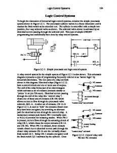
V. TESTING AND VALIDATION Software testing is a critical element of software quality assurance and represents the ultimate review of specification, design, and code generation. Test cases provide the scenarios for which particular software operation is verified. These scenarios are built upon the requirements model developed by the designer of the software. Testing begins 'in the small' and progresses 'to the large' [9]. It means that early testing focuses upon single components and by the end the larger and complex scenarios are evaluated. The testing of current software is executed through the validation of existing circuits made for FSTS C-1. For validation purposes two simple examples are presented from the FSTS C-1 archive. A. SIS Interlock Logic Diagram SCSV43A The diagram presented in Figure 1 of appendix-A shows the interlock logic of controlling a valve in Safety Injection System (SIS) through a single manual switch. This diagram utilizes four binary inputs, one analog signal value, one analog to binary converter, one binary delay, one SRFlipFlop, one manual switch, two AND gates and two OR gates. Starting from the left, an analog signal value and a digital input are shown. Next an analog to binary converter attached with analog signal and a binary delay device attached with binary input are shown. Next comes an AND gate connected with analog to binary converter and binary delay. Next an SR-FlipFlop connected with AND gate and a binary input (as reset signal) is presented. Below this, an AND gate connected with a binary input and the ‘Manual Open’ (MOP) leg of the manual switch is shown. Next two OR gates are presented. The upper one is attached with the output terminal of SR-FlipFlop and the AND gate. However, the lower one is attached solely with the ‘Manual Close’ (MCL) leg of the manual switch.
Paper id: 196
4
B. SIS Interlock Logic Diagram SCSV31A/B The diagram presented in Figure 2 of appendix-A shows the interlock logic of controlling a valve in SIS through two manual switches. This diagram utilizes three binary inputs, four SR-FlipFlops, two manual switches, three AND gates and three OR gates. Starting from the left, a manual switch is shown. Next two SR-FlipFlops attached with the MOP and MCL legs of manual switch are shown. Next comes an AND gate connected with output terminal of second SR-FlipFlop and a binary input. Below this, a replica is shown. Next two OR gates are presented. The upper one is attached with the output terminal upper AND gate and a binary input. However, the lower one is attached with the output terminal lower AND gate and a binary input. Next an AND gate connected with the output terminals of SR-FlipFlop number 1 and 3 is presented. Below the AND gate, an OR gate attached with the output terminal of the other OR gates is presented.
CLCD software. The control and interlock logic designing through CLCD software is verified according to the existing logic archived in FSTS C-1 reference manual. The testing has come out to be successful.
REFERENCES [1]
Tony R. Kuphaldt, “Volume IV-Digital”, All About Circuits Inc., USA, 2008. URL: http://www.allaboutcircuits.com/ vol_4/index.html
[2]
M. Morris Mano, Digital Logic and Computer Design, Prentice Hall Inc., USA, 1979.
[3]
Charles H. Roth, Jr., Fundamentals of Logic Design, 5th Edition, Thomson Learning, USA, 2003.
[4]
Dr Bill Carroll, “Chapter 6 -- Introduction to Sequential Devices”, Department of Computer Science and Engineering, University of Texas, Texas, USA, 2007. URL: http://www.cse.uta.edu/%7Ecarroll/cse2341/fall98/chapter6/ sld017.htm
[5]
John Hewes, “Switches”, The Electronics Club, 2008. URL: http://www.kpsec.freeuk.com/ components/switch.htm
[6]
Adrian Als, “Counters”, Department of Computer Science, Mathematics and Physics, University of West Indies, Barbados, West Indies, 2000. URL: http://scitec.uwichill.edu.bb/cmp/ online/P10F/counters1.htm
[7]
Karl Johan Åström, and Tore Hägglund, PID Controllers: Theory, Design, and Tuning, 2nd edition, Instrument Society of America, USA, 1995.
[8]
Encyclopedia Britannica, Inc., "Signal Generator", Encyclopedia Britannica, Inc., Chicago, USA, 2008. URL: http://www.britannica.com/EB checked/topic/543757/signalgenerator
[9]
Roger S. Pressman, Software Engineering - A Practitioner's Approach, McGraw Hill Companies Inc., New York, USA, 2001.
VI. RESULTS AND CONCLUSIONS Software Simulations play important role in understanding the complex real world problems. Nuclear simulators are the complex systems to model. The development of CLCD software is not an easy task. The design of the software is developed iteratively. The user interface is also changed during the course of development. The CLCD software is a design and model tool for developing control and interlock logic graphically. It achieves the graphical interface model with the help of vector graphics. The use of vector graphics enables the portability feature. The designing through CLCD is at most kept easy and user friendly. The designers of FSTS C-2 can readily become familiar with the easy to design and simulate methodology adapted in CLCD. Additional online simulation control mechanism makes CLCD a powerful designing and simulation tool. The interfacing with the existing nuclear simulation software through que file is strong plus point of
Paper id: 196
5
APPENDIX-A
Figure 1: SIS Interlock Logic Diagram SCSV43A
Figure 2: SIS Interlock Logic Diagram SCSV31A/B