Mar 3, 2014 - 1Mathematical Institute, University of Oxford, Woodstock Rd, Oxford OX2 6GG, United Kingdom. 2Clarendon Laboratory, Department of Physics ...
APPLIED PHYSICS LETTERS 104, 091602 (2014)
Controlling coverage of solution cast materials with unfavourable surface interactions V. M. Burlakov,1 G. E. Eperon,2 H. J. Snaith,2 S. J. Chapman,1 and A. Goriely1 1
Mathematical Institute, University of Oxford, Woodstock Rd, Oxford OX2 6GG, United Kingdom Clarendon Laboratory, Department of Physics, University of Oxford, Parks Road, Oxford OX1 3PU, United Kingdom 2
(Received 8 November 2013; accepted 18 February 2014; published online 3 March 2014) Creating uniform coatings of a solution-cast material is of central importance to a broad range of applications. Here, a robust and generic theoretical framework for calculating surface coverage by a solid film of material de-wetting a substrate is presented. Using experimental data from semiconductor thin films as an example, we calculate surface coverage for a wide range of annealing temperatures and film thicknesses. The model generally predicts that for each value of the annealing temperature there is a range of film thicknesses leading to poor surface coverage. The model accurately reproduces solution-cast thin film coverage for organometal halide perovskites, key modern photovoltaic materials, and identifies processing windows for both high and low levels C 2014 AIP Publishing LLC. [http://dx.doi.org/10.1063/1.4867263] of surface coverage. V There is a broad family of emerging photovoltaics which rely on the processing of uniform thin-films of (poly)crystalline semiconductors from solutions. Such thin films are often thermodynamically unstable and upon post-annealing they tend to partially de-wet the substrate by the growth of pinholes, which may grow further and even break the film into islands (see Ref. 1, and the references therein). The driving force for de-wetting is the minimization of the total energy of the film, the substrate, and of the film-substrate interface. The initial stage of hole nucleation and de-wetting may happen via several mechanisms, both in liquid state during film deposition2 and at the beginning of the annealing process where temperature can accelerate the growth of holes.3 Hole nucleation during film fabrication can be controlled by carefully selecting the solvent and its evaporation rate.4,5 However, the multiple mechanisms of hole nucleation during annealing are less controllable, since most of them are due to largely inevitable imperfections in the film or film-substrate interface structures. The main process decreasing surface coverage of the film during annealing is the growth of holes. Simple models of an isolated cylindrical hole show that it will grow further or collapse depending on the value of its radius relative to some critical value.3 In the complex environment of real films, there are many holes of various sizes that interact with each other by changing the film thickness or the distribution of elastic stress over the film. Moreover, the annealing process is meant to improve the functional properties of the film by removing solvent residues and excess non-stoichiometric volatile components and by improving its crystalline structure. These changes also contribute to possible variations in film thickness and composition during annealing, which further influences the evolution of the holes. While the theoretical description of individual hole growth is well developed,6 little is known on the simultaneous evolution of multiple holes and their cumulative influence on the surface coverage apart from the dilute case where hole-hole interactions can be decoupled.7,8 In this Letter, we also use the dilute assumption to present a robust semi-analytical model, which provides an understanding of the key parameters helping to control and 0003-6951/2014/104(9)/091602/5/$30.00
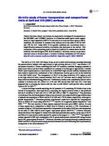
maximize surface coverage by thin films. The model is applied to the photovoltaic material CH3NH3PbI3�xClx. A recent breakthrough in emerging photovoltaics, which has enabled the power conversion efficiency of cells to move beyond 15%,9–13 has taken place in large part due to a novel organic-inorganic compound with perovskite-type crystal structure.14 A solution-processed organolead halide perovskite, CH3NH3PbI3�xClx, is not only an effective photovoltaic sensitizer but can also play the role of an electron transporter when formed from solution within an inert mesoporous alumina scaffold.11 This property enables minimisation of energy losses and a correspondingly high open-circuit voltage of 1.1 V. Subsequent thickness reduction and removal of the mesoporous inert scaffold results in an increase in the photocurrent of the solar cell.10 However, the formation of a uniform solid thin film of the perovskite absorber without the assistance of the mesoporous scaffold cannot be easily realized. In the standard solution-processing technique used to form these films, a non-stoichiometric precursor is spin-coated on a substrate and undergoes subsequent annealing to form the crystalline perovskite. During this annealing, solvent evaporation and stoichiometry-driven mass loss contribute to the formation of holes within the final crystalline layer. Characteristic SEM images of two films of this perovskite deposited by spin-coating on a smooth amorphous TiO2 surface coated upon a c-Si wafer are shown in Fig. 1. As-deposited films obtained after solvent drying but before annealing (a) and (c) look rather smooth. After annealing at 100 � C for 60 min, a granular structure is observed due to hole growth (darker areas in (b) and (d)). Note also that the average hole diameter is much larger for thicker films. From this initial observation and the fact that there is 10%–15% volume loss during annealing, we have developed a model describing the annealing-induced evolution of surface coverage by thin films. The model is based on a few basic assumptions: (i) all holes have cylindrical shape and never impinge upon each other; (ii) the holes are nucleated either before or shortly after annealing starts and nucleation does not take place during
104, 091602-1
C 2014 AIP Publishing LLC V
091602-2
Burlakov et al.
Appl. Phys. Lett. 104, 091602 (2014)
FIG. 1. SEM images of two films of CH3NH3PbI3�xClx on smooth amorphous TiO2-coated silicon substrate. (a) As deposited thin (�50 nm) film; (b) thin film annealed for 1 h at 100 C; (c) as deposited thick (�250 nm) film; (d) thick film annealed for 1 h at 100 C. Film thicknesses (averaged over the covered area) after annealing are 10%–20% lower than those before annealing.
the hole growth/shrinkage process; (iii) elastic stresses in the film are fully relaxed before noticeable change in film morphology takes place, (iv) no discrimination is made between solvent loss, and driven-off non stoichiometric components, since they are de-facto volatile, and we use the generic term “solvent” to describe all mass loss. Then, the surface and interface energy, E, of a film containing N cylindrical holes and sitting on a substrate with the area L � L is given by ! N N X X 2 2 E ¼ cF 2ph Rk þ L � p Rk k¼1 N X
þcI L2 � p
R2k
k¼1
!
dRi ¼ AFL n�ðRi � RC Þ; dt
(3)
where AFL ¼ 2pC1 ðcF þ cIS Þ is the material flow rate per unit solvent concentration, and RC ¼ hðtÞ=ð1 þ cIS =cF Þ is a time-dependent critical radius for hole growth. With solvent evaporation, the film volume changes according to the equation dV ¼ �AEV ns a3 L2 ; dt
(4)
k¼1 N X þ cS p R2k ;
(1)
k¼1
where h is the film thickness; cF , cS , and cI are surface energies of film, substrate, and the film-substrate interface energy, respectively; and Ri are the radii of the holes. Assuming a gradient flow of energy, the time evolution of holes radii is given by dRi dE ¼ �C ¼ �2pCðcF h � Ri ðcF þ cIS ÞÞ; dt dRi
where ns ¼ nðh; tÞ is the solvent concentration at the film surface, a3 is an average molecular volume in the film material, and AEV ns is the molecular evaporation rate per unit surface area. Here, we neglect solvent evaporation from the side walls of the holes and the change in the film area due to the holes, i.e., we consider the high coverage limit, expressed by the condition N 1 X p R2 � 1: L2 i¼1 i
(5)
(2)
where cIS ¼ cI � cS and C is the kinetic coefficient which depends on the particular physical mechanisms of material flow. To account for the presence of solvent in the film, we may represent the kinetic coefficient as consisting of two components, C ¼ C0 ðn0 � n�Þ þ C1 n�, with C0 accounting for pure material flow and C1 accounting for that mediated by the solvent, which has an average concentration of n� and a maximum concentration of n0. At typical temperatures used for annealing (�100 � C), the pure film material does not flow. Therefore, we assume that the holes change size only due to the presence of solvent, i.e., C � C1 n�, and (2) takes the form
To close the system, we express the concentration at the surface ns in terms of the average volume fraction n�. The solvent concentration inside the film is described by @n @2n ¼D 2; @t @z D D
0 < z < h;
@n ¼ 0 on @z
@n ¼ �AEV n @z
z ¼ 0; on
z ¼ h;
(6) (7) (8)
where D is the temperature dependent diffusion coefficient for the solvent. In the case of slow evaporation
091602-3
Burlakov et al.
Appl. Phys. Lett. 104, 091602 (2014)
(P � hAEV =D � 1), the evolution is quasistatic, the concentration profile across the film is close to quadratic, and it can be shown that ns and n� are related by � � hAEV ns : (9) n� � 1 þ 3D Under the approximation (9), the average concentration evolves according to d� n AEV n�AEV ns � � : ¼� h hð1 þ hAEV =3DÞ dt
(10)
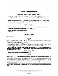
If the thickness h is assumed to vary slowly with time, it can be assumed constant with respect to the typical time scale for the variation of n so that the n ¼ nðtÞ is � solution for��1 n�ðtÞ ¼ n�ð0Þe�bt , where b ¼ AEV h þ h2 AEV =3D . The validity of the approximation (9) can be assessed by comparing this expression with the actual decay of n�. The results, presented in Fig. 2, show that the approximation is good even when P is as large as 10. Within the approximations given by (5) and (9), it is possible to study the film coverage as a function of the film thickness. Dividing (3) by (4) and using (9) and V ¼ hL2 gives � � �� dRi AFL h hAEV ¼� 3 ; (11) Ri � 1þ dh a AEV 3D 1 þ cIS =cF with solution � � 2 2 Ri ðhÞ ¼ R i ðhÞ þ Ri ðh0 Þ � R i ðh0 Þ e�c0 ðh�h0 Þ�c1 ðh �h0 Þ ; (12) where c0 ¼
AFL ; a3 AEV
c1 ¼
AFL ; 6a3 D
c2 ¼ 1=ð1 þ cIS =cF Þ;
� � pffiffiffiffiffi c2 c0 R ðhÞ ¼ c2 h � pffiffiffiffiffi F pffiffiffiffiffi þ c1 h ; 2 c1 c1 FðnÞ ¼ e
�n2
ðn
g2
e dg: 0
FIG. 2. Simulated time evolution of the average solvent concentration during its evaporation from one side of a film of constant thickness h (solid lines) compared to the simplex exponential approximation (10) (dashed lines) for P ¼ 0.1 (1), 1 (2), and 10 (3).
This solution implies that the hole size distribution remains Gaussian, if it was initially Gaussian. Indeed, starting with an initial Gaussian distribution f0 ðRÞ ¼ Z �1 expð�ðR � R0 Þ2 =2r2 Þ and writing Rðh0 Þ in terms of R(h) leads to a final Gaussian distribution fa ðRÞ ¼ Z1�1 expð�ðR � R1 Þ2 =2r21 Þ; R1 ¼ R ðhÞ þ aðR0 � R ðh0 ÞÞ;
r1 ¼ ar;
(13)
where ln a ¼ c0 ðh0 � hÞ þ c1 ðh20 � h2 Þ. The Gaussian distribution (13) has a shifted peak position R1 and a renormalized width r1 . We use here a single Gaussian distribution, but the self-similarity of the distribution of hole sizes is also applicable to the more generic case when the initial distribution is represented by a sum of Gaussians. Using (13) and taking a volume loss of 10% such that h ¼ 0:9h0 , we can now readily compute the surface coverage Cðh0 ; TÞ as a function of the initial film thickness h0 and the annealing temperature T without the need to perform expensive simulations of the evolution of multiple holes. First, we determined experimentally the distribution of hole sizes before annealing from SEM images of CH3NH3PbI3�xClx films deposited on smooth TiO2 substrates shown in Figs. 1(a) and 1(c) using the software ImageJ.15 Typically, this experimental distribution (see Fig. 3) is characterized by many holes assigned the same size and can be approximated by a Gaussian of the form f0 ðRÞ ¼ Z �1 expð�ðR � R0 Þ2 =2r2 Þ with R0 ¼ 115 nm and r ¼ 125 nm. This Gaussian then evolves to that given in (13) under annealing, which is used to determine the film coverage as a function of the parameter a via ð ð R2 fa ðRÞ dR 1 2 ; CðaÞ ¼ 1 � 2 R fa ðRÞ dR ¼ 1 � ð1 � C0 Þ ð L R2 f0 ðRÞ dR (14) where C0 is the film coverage before annealing, which we take to be 90%. As the value of cIS =cF is unknown, we considered several values from the range ð�1; 1Þ and selected cIS =cF ¼ 0:54 as the best fit to experimental data.16 We now
FIG. 3. Distribution of hole radii (symbols) before annealing obtained by averaging over 10 samples of thicknesses 200–600 nm. Solid line shows Gaussian distribution with the parameters R0 ¼ 115 nm and r ¼ 125 nm.
091602-4
Burlakov et al.
fit CðaÞ to three experimental data points using the least squares method to determine the parameter values c0 ¼ 40:10 lm�1 and c1 ¼ 15:17 lm�2 for a given annealing temperature T ¼ 100 � C ¼ 0.032 eV. Note that the ratio c1 =c0 ¼ AEV =6D ¼ 0:378 lm�1 gives the value of P ¼ hAEV =D ¼ 2:27 (for h ¼ 1 lm), for which the approximation (9) is good. The next step in calculating Cðh0 ; TÞ is to obtain the temperature dependence of c0 and c1. These can be written in the form � � EFL � EEV c0 ðTÞ ¼ c00 exp � ; (15a) kB T � � EFL � EDI ; (15b) c1 ðTÞ ¼ c10 exp � kB T where c00 and c10 are constant, and EFL, EEV, and EDI are activation energies for material flow, solvent evaporation, and solvent diffusion, respectively. The difference in activation energies is obtained fitting to additional experimental data related to film annealing at 85 � C and 120 � C and is found to be EFL � EEV ¼ 0:02274 eV, EFL � EDI ¼ 0:02270 eV. Once the four parameters c00, c10, EFL � EEV and EFL �EDI entering (14) are known, we can contour plot Cðh0 ; TÞ as shown in Fig. 4. According to this model, at a given annealing temperature, the coverage first decreases with increasing initial film thickness and then increases, reaching the highest levels with the thickest films and the lowest annealing temperatures. In particular, for an annealing temperature suitable for crystallization of the compound CH3NH3PbI3�xClx (� 100 � C (Ref. 11)), our model suggests that it would be difficult to achieve coverage higher than 70% for films thinner than 500 nm. To obtain coverage over 85%, the film must be either much thicker (>900 nm) or much thinner (