www.afm-journal.de
www.MaterialsViews.com
Xiaoshuang Chen, Guangbo Liu, Wei Zheng, Wei Feng, Wenwu Cao, Wenping Hu,* and PingAn Hu*
full paper
Vertical 2D MoO2/MoSe2 Core–Shell Nanosheet Arrays as High-Performance Electrocatalysts for Hydrogen Evolution Reaction
electrochemical water splitting is in the quest for each-abundant, highly catalytical materials for hydrogen evolution reaction (HER) in the place of earth scarce, expensive platinum (Pt) and precious metal oxides. 2D transition metal dichalcogenide (TMDs, MoS2, MoSe2, etc.) have been recognized as low cost catalyst alternatives for HER reaction because of their earth abundant composition[3,4] and highly catalytic activity.[4,5] The catalytic performance of TMD materials for HER mainly relies on the catalytic site numbers (defects at edges or planes) and conductivity as well as the efficient exposure surface. The conductivity of catalyst that benefits the charge transfer for proton reduction, is determined by the used component, crystallinity, and electrical contact between catalytic materials and the conductive substrate. The exposure surface, which benefits for HER reaction, was closely associated with nanostructured architecture at the electrode (e.g., vertical nanosheet arrays). To date, several strategies were demonstrated to improve the catalytic activity including increasing the defect numbers by chemical doping,[6] boosting conductivity by phase transformation,[7] or mixing with metallic materials (e.g., graphene),[8–11] and efficiently exposing active sites by fabricating vertical MoS2.[12] For example, Xie et al. demonstrated high performance defect-rich MoS2 for HER reaction by oxygen incorporation.[6] Jin et al. reported highly active electrocatalysts based on conducting metallic MoS2,[7] and metallic MoS2 facilitates the recovery of its semiconducting 2H type only above 95 °C.[7,13] Cui et al. demonstrated that the vertical oriented MoS2 or MoSe2 on a conductive substrate can efficiently expose the catalytic sites to electrolytes so as to enhance the HER reaction on electrodes,[12] but semiconducting MoS2 or MoSe2 with low conductivity still limit their performance. Thus far, those 2D TMDs (MoS2, MoSe2) electrodes in electrochemical water splitting devices were mostly fabricated by depositing exfoliated sheets suspensions onto conductive substrate. This solution processed fabrication produced inevitable agglomeration and re-stacking of MoS2 or MoSe2 nanosheets as well as not fine electrical contacts between nanosheet film and conductive substrates, whereas chemical vapor deposition (CVD) method that can grow high crystalline materials with intimate
Electrochemical water splitting is very attractive for green fuel energy production, but the development of active, stable, and earth-abundant catalysts for the hydrogen evolution reaction (HER) remains a major challenge. Here, core–shell nanostructured architectures are used to design and fabricate efficient and stable HER catalysts from earth-abundant components. Vertically oriented quasi-2D core–shell MoO2/MoSe2 nanosheet arrays are grown onto insulating (SiO2/Si wafer) or conductive (carbon cloth) substrates. This core–shell nanostructure array architecture exhibits synergistic properties to create superior HER performance, where high density structural defects and disorders on the shell generated by a large crystalline mismatch of MoO2 and MoSe2 act as multiple active sites for HER, and the metallic MoO2 core facilitates charge transport for proton reduction while the vertical nanosheet arrays ensure fully exposed active sites toward electrolytes. As a HER catalyst, this electrode exhibits a low Tafel slope of 49.1 mV dec−1, a small onset potential of 63 mV, and an ultralow charge transfer resistance (Rct) of 16.6 Ω at an overpotential of 300 mV with a long cycling durability for up to 8 h. This work suggests that a quasi 2D core–shell nanostructure combined with a vertical array microstructure is a promising strategy for efficient water splitting electrocatalysts with scale-up potential.
1. Introduction Electrochemical water splitting is a carbon-free approach to produce green fuel energy of hydrogen gas, has been attracted widespread research interest.[1,2] The central problem in Dr. X. S. Chen, Dr. G. B. Liu, Dr. W. Zheng, Dr. W. Feng, Prof. P. A. Hu Key Lab of Microsystem and Microstructure of Ministry of Education Harbin Institute of Technology Harbin 150080, P. R. China E-mail:
[email protected] Dr. X. S. Chen, Prof. W. W. Cao, Prof. W. P. Hu Department of Physics Harbin Institute of Technology Harbin 150080, P. R. China E-mail:
[email protected] Prof. W. P. Hu Key Laboratory of Organic Solids Institute of Chemistry Chinese Academy of Sciences Beijing 100190, P. R. China
DOI: 10.1002/adfm.201603674
Adv. Funct. Mater. 2016, 26, 8537–8544
© 2016 WILEY-VCH Verlag GmbH & Co. KGaA, Weinheim
wileyonlinelibrary.com
8537
www.afm-journal.de
full paper
www.MaterialsViews.com
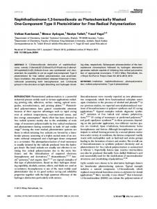
Figure 1. a) Schematic illustration of the formation of vertical core–shell MoO2/MoSe2 nanosheet arrays, b) XRD patterns, and c) Raman spectra of MoO2 and core–shell MoO2/MoSe2 nanosheet arrays on different substrates.
contacts toward substrate, have been scarcely investigated in producing 2D TMDs electrodes for HER. Especially, there is lack of strategy thereby combining the aforementioned three aspects (rich defects, high conductivity and efficient exposures of active sites) into one HER catalyst fabrication of 2D layered materials. To address those problems, we propose a proof of concept strategy to design and fabricate ultra-high performance HER catalysts using the combination of quasi 2D core–shell nanostructure and vertical array microstructure, which is realized by a CVD method. Core–shell nanostructures (CSNs) have attracted considerable interests in creating numerous advanced crystals with attractive properties and functions in the past decade.[14,15] CSNs consist of cores (inner material) and shells (outer layer material) both at nanoscale. The physical properties of CSNs can be tailored through the controlling the inner or outer layer components.[14] Moreover, CSNs may produce synergistic physical and chemical properties that are much improved over each single-component counterparts alone.[15] Therefore, a variety of functional core–shell nanostructures have been fabricated to meet the need for solar cells, optoelectronics and catalysts etc.[14,16–18] Thus far, most functional core–shell nanostructures are grown into spherical shape (nanoparticle),[19] a rod/ nanowire shape (1D structure),[20,21] or a disk shape (dot in plate core/shell structure),[22] whereas quasi 2D core–shell nanostructure has been scarcely reported. Moreover, aligned 2D core–shell nanosheet arrays for applications in catalysts for electrochemical water splitting have not been realized up to date. In this article, we demonstrate that wafer-scale vertically aligned core–shell MoO2/MoSe2 nanosheet arrays can be synthesized on insulating (SiO2/Si) or conductive (carbon cloth) substrate via a continuous two-step CVD process. The morphologies, structures, and chemical composition of these 2D core–shell nanostructures are characterized by using scanning 8538
wileyonlinelibrary.com
electron microscopy (SEM), X-ray diffraction (XRD), and transmission electron microscopy (TEM). The electrochemical measurement showed that the core–shell MoO2/MoSe2 nanosheet array electrode exhibits a small Tafel slope of 49.1 mV dec−1, a low onset potential (0.063 V vs reversible hydrogen electrode (RHE)), a small overpotential of 0.181 V versus RHE at a current density of 10 mA cm−2 and a high conductivity as well as outstanding cycle stability. This superior performance is attributed to the synergistic properties from core–shell MoO2/ MoSe2 nanostructure combined with the array microstructure, in which the defect-rich MoSe2 outlayer acted as an efficient catalyst, and the conductive MoO2 inner facilitated charge transport to electrode while vertically standing nanosheet arrays fully exposed the catalytic sites to electrolytes. Consequently, vertically oriented MoO2/MoSe2 core–shell architecture has the potential to be the succedaneum of noble metals for HER application.
2. Results and Discussion Figure 1a illustrates the two-step procedure for growing vertically oriented core–shell 2D MoO2/MoSe2 nanosheet arrays. First, vertical MoO2 nanosheet arrays were grown onto substrate (SiO2/Si, carbon cloth) using MoO3 and H2 gas by the CVD method; second, the as-grown vertical MoO2 nanosheet arrays were calcined in Se vapor to form a MoSe2 out-layer. Each-step evolutions were characterized by using XRD and Raman spectroscopies (shown in Figure 1). Figure 1b shows the XRD patterns of vertical MoO2 nanosheet arrays and core– shell MoO2/MoSe2 nanosheets on SiO2/Si or carbon cloth (CC) substrates. All peaks (≈26.0°, 31.6°, 36.7°, 41.6°, and 53.5° 2θ) obtained from the oxides nanosheet arrays (on both SiO2/Si and CC substrate) correspond well to monoclinic crystalline molybdenum dioxide (JCPDS Card No. 32-0671), which
© 2016 WILEY-VCH Verlag GmbH & Co. KGaA, Weinheim
Adv. Funct. Mater. 2016, 26, 8537–8544
www.afm-journal.de
www.MaterialsViews.com
with an average height of 1–3 μm as well as a top and bottom edge lengths of 1–3 and 4–7 μm, respectively (Figure 2c,d). The density of vertical MoO2 nanosheet on SiO2/Si substrate was calculated to be ≈6 flakes per 100 μm2 (Figure 2a–d), and much denser MoO2 nanosheets (≈24 in 1 μm2 area) were grown onto the carbon cloth substrate (Figure 2i–l). As shown in Figure 2i–l, the entire surface of the carbon cloth was covered with high density MoO2 nanosheets. And these nanosheets on carbon cloth have a much smaller size (≈0.3 μm in dimension) than on SiO2/Si. The high density and small dimension products on carbon cloth substrate are attributed to the crude surface of the growth substrate, which leads to dense nucleation sites (Figure S1, Supporting Information). As shown in Figure S2a,b in the Supporting Information, the thickness of MoO2 nanosheet is ≈30 nm, identified by atomic force microscopy (AFM). Figure 2e–h, m–p and Figure S2c,d in the Supporting Information are the photographs, SEM and AFM images of vertically oriented core–shell MoO2/MoSe2 nanosheet arrays on SiO2/Si and carbon cloth substrates. Their morphologies (trapezoid-like shape), dimensions (e.g. growth on SiO2/Si, an average height
full paper
indicates the formation of MoO2 crystals with a favorable growth direction of [200] by the virtue of the strongest peak of (200). After selenylation calcination, the peaks for the original monoclinic crystalline phase of MoO2 remained in XRD results, and accompanying peak (≈13.6° 2θ) belongs to hexagonal MoSe2 (JCPDS Card No. 29-0914), indicating the formation of core–shell MoO2/MoSe2 nanosheet. The samples at each-step were further characterized by Raman spectroscopy (Figure 1c). Raman characteristic peaks for selenylation products displayed in the range of 180–800 cm−1 were assigned to MoSe2 (A1g mode ≈238 cm−1 and E2g mode ≈284 cm−1)[23] and MoO2 (≈205, 229, 347, 365, 498, 572, and 745 cm−1)[24,25] respectively, while no Raman characteristic peaks of hexagonal MoSe2 were observed from the products without treating in selenium vapor. SEM was used to investigate the morphology and structure of as-prepared vertically oriented MoO2 and core–shell MoO2/MoSe2 nanosheet arrays on different substrates. In Figure 2a–d, the as-grown MoO2 nanosheets were normal to the SiO2/Si substrate. These nanosheets have a trapezoid-like shape
Figure 2. Photographs and SEM images of vertical MoO2 and core–shell MoO2/MoSe2 nanosheet arrays on different substrates. a–d) MoO2 nanosheets on SiO2/Si substrate, e–h) core–shell MoO2/MoSe2 nanosheets on SiO2/Si substrate, i–l) MoO2 nanosheets on carbon cloth substrate, and m–p) core–shell MoO2/MoSe2 nanosheets on carbon cloth substrate.
Adv. Funct. Mater. 2016, 26, 8537–8544
© 2016 WILEY-VCH Verlag GmbH & Co. KGaA, Weinheim
wileyonlinelibrary.com
8539
full paper
www.afm-journal.de
8540
www.MaterialsViews.com
is 1–3 μm, top edge is 1–3 μm, and bottom length of 4–7 μm), and thickness (≈30 nm) are almost unchanged compared to the corresponding vertical MoO2 nanosheets. The origin for the vertical growth of MoO2 nanosheets (also core–shell MoO2/MoSe2 nanosheets) onto various substrates might be attributed to the intrinsic characteristics of crystal structure of the monoclinic MoO2. The surface energies (γ) of (100), (010), (001), and (101) planes of monoclinic MoO2 are calculated to be γ(100) = 7.38 J m−2, γ(010) = 7.45 J m−2, γ(001) = 7.40 J m−2, and γ(101) = 4.28 J m−2 (calculation details are in the Supporting Information). It is noted that (101) lattice plane has the lowest surface energy while (100), (010), and (001) lattice planes have similar surface energy. Consequently, (100), (010), and (001) lattice planes can grow faster on substrates to form vertical structures and serve as the marginally bared covers in the final structure, while the (101) lattice plane shows a slow growth speed and serves as the surface facet of the 2D nanosheet. A proposed growth schematic illustration of vertical MoO2 nanosheets is displayed in Figure S3 in the Supporting Information. TEM was used to investigate the core–shell structure and composition distribution of pristine MoO2 and MoO2/MoSe2 nanosheet arrays. As shown in Figure 3a–c, a typical trapezoid-like pristine MoO2 nanosheet has a top edge length of ≈2 μm, a bottom edge length of ≈6 μm, and a height of ≈2 μm (Figure 3a). The lattice spacing of 0.24 nm in high-resolution TEM (HRTEM) (Figure 3b) image corresponds to the (200) plane of monoclinic MoO2, and its chemical composition was composed of oxygen and molybdenum with an atomic ratio of Mo:O = 1:2 by energy-dispersion X-ray spectroscopy (EDX) analysis (Figure S4, Supporting Information). The selected area electron diffraction (SAED) (Figure 3c) displays oneset regularly arranged diffraction spots that are assigned to (200), (−301) planes of monoclinic MoO2. Further, core–shell MoO2/MoSe2 nanosheets were also characterized by TEM (Figure 3d–k). This core–shell nanosheet in low magnification image (Figure 3d) shows similar morphology and dimension to the pristine MoO2 nanosheet (Figure 3a). Furthermore, in the HRTEM image (Figure 3e), it reveals a core−shell architecture judged by the distinct lattice fringes contrast. The ≈10 nm thick MoSe2 out-layer (shell) clearly shows lamellar structure with a layer number of 16. This lamellar structure has a layer spacing of 0.65 nm which is consistent with the (002) plane of hexagonal MoSe2, and the lattice spacing of 0.28 nm on the planar surface corresponds to the (100) plane of MoSe2 (Figure 3e). The SAED pattern (Figure 3f) taken from inner area displays a two-set regularly arranged diffraction spots that are assigned to (100), (110) planes of hexagonal MoSe2, and (200), (−301) planes of monoclinic MoO2, respectively. This two-set SAEDs indicate the formation of a core–shell structure. To further confirm the core–shell structure of MoO2/MoSe2 nanosheet, cross-section TEM nanosheet was prepared by focused ion beam (FIB). The vertical core–shell MoO2/MoSe2 nanosheet was made lying on the 300 nm SiO2/Si substrate before FIB. Cross-sectional TEM images (Figure 3g and Figure S5a, Supporting Information) show the obvious core–shell structure by different color contrast. The shell district exhibits the darker color and the core region displays the lighter color. And the thickness of nanosheet is ≈30 nm in keeping with the AFM
wileyonlinelibrary.com
results. Cross-sectional HRTEM image (Figure 3h) reveals the diverse lattice fringes. The lattice spacing of 0.28 nm in core MoO2 region corresponds to the (101) plane of monoclinic MoO2. The cross-sectional MoSe2 shell area clearly shows lamellar structure with 0.65 nm lattice spacing ((002) plane of hexagonal MoSe2) of ≈3 nm thick thinner than the top-edge (≈10 nm thick) of the vertical MoO2/MoSe2 nanosheet, because of the (100) plane (γ(100) = 7.38 J m−2) of monoclinic MoO2 is more active than (101) plane (γ(101) = 4.28 J m−2) to selenylation process. Therefore, the degree of selenylation on the edge (100) plane is larger than on the surface (101) plane of the nanosheet during the selenylation process. And the compositional distribution of this core–shell nanosheet was studied by high-angle annular dark-field (HAADF, Figure 3j) scanning transmission electron microscopy (STEM) combined with EDX element mapping analysis (Figure 3k–m and Figure S5b–e, Supporting Information). We found that the Mo element (Figure 3k, azure) was homogeneously distributed over the nanosheet while the content of Se element (Figure 3l, green) was higher in the marginal region (judged by color intensity), and the oxygen element (Figure 3m, orange) was comparatively higher in the core area. The shell district was made up of Mo and Se elements while the core area was composed of Mo, Se, and O as shown in EDX spectra of Figure S6 in the Supporting Information. Cross-section elemental mapping images (Figure S5b–e, Supporting Information) displaying the spatial distribution of Mo, O, Se, and Si elements, respectively. Mo element evenly distributed over the cross-section. Se element was located in the edge and the partial O element was situated in the center of the cross-section. The Si and the other O elements derive from the substrate. By the virtue of above structural and compositional analyses, we confirmed that this sheet consisted of MoO2 core and MoSe2 shell. In contrast, no shell structure and Se element were observed from the pristine MoO2 nanosheet by TEM characterization combined with EDX analysis (shown in Figure 3a–c and Figure S4, Supporting Information). To combine all the results of XRD, HRTEM, and composition distribution, the crystalline structure of core–shell MoO2/MoSe2 nanosheet can be described in a schematic diagram (Figure 3i), where the (100) and (101) planes of the MoO2 were interfaced with the (001) plane of the MoSe2 in core–shell nanosheet. The core–shell MoO2/MoSe2 nanosheet was found to have rich structural defects including disordered atomic arrangement, dislocations, distortions and Moire´ patterns. These defects were observed by HRTEM (Figure 4a–e) in different regions. The formation of these defects (e.g., disordered atomic arrangement) is attributed to the altitudinal lattice mismatch (f) of 41.4% between monoclinic MoO2 and hexagonal MoSe2 (calculated by f = (aMoO2 − aMoSe2 )/aMoO2 , a-cell parameter, aMoO2 = 5.6068 Å, aMoSe2 = 3.287 Å). These abundant defect structures can act as catalytically active sites for HER.[26] The disordered degree of atomic arrangement and the rotational angle between single nanodomains can be calculated by the fast Fourier transform (FFT) pattern of the HRTEM images. The FFT patterns (insets of Figure 4a,b) display six different diffraction arcs with different arc length, suggesting a quasiperiodic arrangement of nanodomains with different disordered degrees.[6] The disordered degree can be assessed by the angle obtained from two terminal points of a diffraction arc and the
© 2016 WILEY-VCH Verlag GmbH & Co. KGaA, Weinheim
Adv. Funct. Mater. 2016, 26, 8537–8544
www.afm-journal.de
www.MaterialsViews.com
full paper Figure 3. Core–shell architecture of vertical pure MoO2 and MoO2/MoSe2 nanosheet arrays. a) A low magnification TEM image, b) the corresponding HRTEM image in the edge, and c) SAED pattern of MoO2 nanosheet. d) A low magnification TEM image, e) the corresponding HRTEM image in the edge, f) SAED pattern, g) a low magnification cross-sectional TEM image, h) the corresponding cross-sectional HRTEM image in the edge, i) the connection schematic diagram of the MoO2 core and the MoSe2 shell, and j–m) HAADF-STEM and EDX elemental mapping images of core–shell MoO2/MoSe2 nanosheet.
Adv. Funct. Mater. 2016, 26, 8537–8544
© 2016 WILEY-VCH Verlag GmbH & Co. KGaA, Weinheim
wileyonlinelibrary.com
8541
www.afm-journal.de
full paper
www.MaterialsViews.com
Figure 4. Structural defects and disorders of vertical core–shell MoO2/ MoSe2 nanosheet arrays. a,b) HRTEM images of vertical core–shell MoO2/ MoSe2 nanosheet arrays in different regions, Inset: the corresponding FFT patterns, c) Enlarged HRTEM image of part in (a), d) a low magnification cross-sectional TEM image, and e) enlarged cross-sectional HRTEM image of part in (d).
obvious cathodic current could be observed using core–shell MoO2/MoSe2 and pure MoSe2 nanosheet electrode, and core– shell MoO2/MoSe2 nanosheet electrode displayed a lower onset potential of 0.063 V (vs RHE). A smaller overpotential of 0.181 V (vs RHE) was obtained from the polarization curve (iR-corrected) at 10 mA cm−2 current density. The Tafel slope represents the intrinsic nature of electrocatalysts and manifests the ratio-determining pace in the HER procedure, hence it is considered as the central performance parameter for HER. A smaller Tafel slope implies a faster augment of hydrogen production efficiency with enhanced overpotential applied, which is beneficial for practical applications. The Tafel slopes of the linear fit portions (dark lines of dashes) of the Tafel patterns (Figure 5b) was derived from the Tafel equation, η = blog j + a, where η is the overpotential, j is the current density, and b is the Tafel slope.[8] A smaller Tafel slope of 49.1 mV dec−1 was calculated using the vertical core–shell MoO2/MoSe2 than pure MoSe2 (84.3 mV dec−1) nanosheet array electrode in HER. This Tafel slope value was the lowest among the reported MoSe2 electrocatalysts (59.8–105 mV dec−1).[4,12,27–29] The exchange current density was determined to be 1.36 × 10⁻³ mA cm−2 by fitting the linear portion of the Tafel plot at low cathodic current to the Tafel equation, which is ≈4 fold larger than that obtained from electrocatalyst of single component vertical MoSe2 nanofilms in the previous report (0.38 × 10⁻³ mA cm−2).[4] These observed small Tafel slope and large exchange current density indicate that the architecture of core–shell MoO2/MoSe2 nanosheet arrays can produce superior activity in HER, which will be beneficial for practical applications. In acidic medium, three principle procedures from H+ to H2 conversion for HER have been suggested.[6,26] The first procedure is named Volmer reaction (primary discharge):
middle spot. In other words, the angle of 60° stands for completely disordered atomic arrangement, while 0° stands for ideal single crystal without tortuosity.[6] For convenience, the disordered degrees for diverse positions were standardized by 60°, resulting in the relative disordered degrees quantified by percentage.[6] Therefore, the FFT patterns in Figure 4a,b show disordered degrees of ≈65.2% and 42.3%. The average disordered degree is 53.8%. The higher disordered degree implies more defect structures in the core–shell nanosheet. Partial enlarged HRTEM image (Figure 4c) clearly shows high density structural defects and disordered atomic arrangement on the surface of the core–shell MoO2/MoSe2 nanosheet. Enlarged cross-sectional HRTEM image (Figure 4e) of part in Figure 4d with imperfect layer-by-layer stacking (dislocations, distortions) of MoSe2 shell further displays rich structural defects on core–shell MoO2/MoSe2 nanosheet. Electrocatalytic HER measurements were performed on the vertical core–shell nanosheet arrays on the carbon cloth in 0.5 m H2SO4 solution with a three-electrode electrochemical device. As shown in Figure 5a, the bare carbon cloth and pristine MoO2 nanosheet arrays exhibited almost Figure 5. HER performance of vertical core–shell MoO2/MoSe2 nanosheet arrays on carbon no HER activity because there was hardly cloth substrate. a) Polarization curves, b) the corresponding tafel plots, and c) Nyquist plots any reduction current until the electrode at different overpotentials, the inset is the Randles equivalent circuit. d) Stability test for 2000 potential reached 0.35 V (vs RHE), whereas continuous cycles. 8542
wileyonlinelibrary.com
© 2016 WILEY-VCH Verlag GmbH & Co. KGaA, Weinheim
Adv. Funct. Mater. 2016, 26, 8537–8544
www.afm-journal.de
www.MaterialsViews.com
Adv. Funct. Mater. 2016, 26, 8537–8544
in previous reports.[11,26] All results suggested that the vertical core–shell MoO2/MoSe2 nanosheet arrays had an outstanding HER performance, compared to other non-noble metal MoSe2based catalysts (Table S1, Supporting Information). The remarkable HER performance obtained from our nanosheet samples is attributed to the synergistic properties caused by the combination of core–shell nanostructure and the vertical array microstructure. The rich defects in the surface of MoSe2 shell acted as numerous catalytic sites for HER in electrochemical water splitting while the metallic MoO2 core facilitates to electron transport for photon reduction, simultaneously increasing the HER performance. Additionally, the vertical array structure allows for full exposure of the catalytic sites to the reactive electrolytes to boost HER process.
full paper
H3O+ + e− → Hads + H2O. And then Heyrovsky reaction (electrochemical desorption): Hads + H3O+ + e− → H2 + H2O or Tafel reaction (recombination): Hads + Hads → H2 may be included. Under a given set of conditions, when Volmer reaction is HER rate-limiting procedure, 120 mV dec−1 slope can be generated, while if Heyrovsky or Tafel reactions serve as the rate-limiting procedure, 30 and 40 mV dec−1 Tafel slopes should be received, respectively.[6,26] The calculated Tafel slop is 49.1 mV dec−1 in our study, and the combination of Volmer–Heyrovsky or Volmer–Tafel mechanism is therefore proposed for the H2 evolution process using core–shell MoO2/MoSe2 nanosheet array electrode. Electrochemical impedance spectroscopy (EIS) is a powerful tool for investigating the as-constructed electrodes/solution interface reactions and electron transfer kinetics in the HER process. The Nyquist plots (Figure 5c) of the vertical core– shell nanosheet exhibited an obvious decrease of the charge transfer resistance (Rct) with increasing overpotentials over the frequency range from 0.1 Hz to 105 Hz, which was confirmed by the decrease of the diameter of the semicircles. More detail discussions were conducted by fitting the impedance data to a facile Randle equivalent circuit (Figure 5c inset).[6] A constant phase element was used for this fitting procedure. The Rct of as-prepared nanostructured electrodes was reduced when the overpotential was increased from 40.8 Ω (at 150 mV) to 16.6 Ω (at 300 mV). The series resistances (Rs) were all ≈3.3 Ω independent of overpotentials. This low resistance was mainly originated from the conductive inner MoO2 and the intimate contact between products with the carbon cloth substrate that was formed by the direct CVD growth. Such low resistance benefits the electron transport to form proton reduction at electrode surface, and boosts the HER. To estimate the effectively electrochemical active surface area of vertical core–shell MoO2/MoSe2 nanosheet array catalyst, the cyclic voltammetry (CV) technique was executed to obtain the electrochemical double-layer capacitance (Cdl), which is supposed to be linearly proportional to the effectively electrochemical active surface area.[5,30,31] CV curves (Figure S7a, Supporting Information) of vertical core–shell MoO2/MoSe2 nanosheet array catalyst were measured at 0.1–0.2 V versus the RHE range with different scan rates (20, 40, 60 mV s−1, etc.). The Cdl was acquired by plotting the current density difference j at the middle of the scanning potential region (at 0.15 V vs RHE) versus the scan rate, where the slope is double Cdl. As shown in Figure S7b in the Supporting Information, the vertical core–shell MoO2/MoSe2 nanosheets display the biggish Cdl of ≈18.68 μF, suggesting the high exposure of efficient active sites, which is accountable for the outstanding HER performance. The core–shell nanostructure electrode displayed good stability in HER measurement. As shown in Figure 5d, the cathodic current density showed almost no change in the polarization curves of continuous operation before and after 2000 cycles at a scan rate of 50 mV s−1. Furthermore, a continuous chronoamperometric curve (Figure S8, Supporting Information) also displayed almost no degradation in the current density under static overpotential of 0.19 V for 30 000 s, and there appeared some spike-like shapes along this chronoamperometric curve, which are due to the alternate procedures of hydrogen bubble accumulation and release. Similar phenomena were observed
3. Conclusion In conclusion, vertically oriented core–shell array architecture of MoO2 core and MoSe2 shell nanosheet was synthesized through a two-step growth procedure. This vertically aligned core–shell MoO2/MoSe2 nanosheet arrays have some advantageous characteristics for the HER application including abundant defects at surfaces, high conductivity, and fully exposing active sites to reactive electrolytes, all contribute to the high performance HER. In the HER process, this core–shell array electrode exhibited a low Tafel slope of 49.1 mV dec−1, small onset potential of 63 mV, an ultralow charge transfer resistance (Rct) of 16.6 Ω at overpotential of 300 mV and an long cycling durability. Our research provides a new promising strategy for scale-up fabrication of efficient and stable HER electrocatalysts bases on quasi 2D core–shell nanostructure combined with vertical array microstructure.
4. Experimental Section Two-Step Growth of Vertically Oriented Core–Shell MoO2/MoSe2 Nanosheet Arrays: The setup was a typical CVD system consisting of a clean quartz tube and a tube furnace with an independent temperature controller. First, vertical MoO2 nanosheet arrays were grown on the substrate (SiO2/Si, carbon cloth) by a CVD process using commercial molybdenum oxide powder (MoO3, 99.9%, 35 mg, Aladdin). The reaction was performed in the presence of mixed H2/Ar gases (7/8 sccm) at 400–780 °C for 20 min; second, commercial selenium powder (Se, 99.99%, 0.6 g, Aladdin) was evaporated at 300 °C, and the as-grown vertical MoO2 nanosheet arrays were calcined in Se vapor at 600–900 °C for ≈30 min to form core–shell MoO2/MoSe2 and pure MoSe2 nanosheet arrays. After the growth, the furnace was naturally cooled down to room temperature. The schematic illustration of the synthesis process of vertically oriented core–shell MoO2/MoSe2 nanosheet arrays is displayed in Figure S9 in the Supporting Information. Structure and Morphology Characterization: The purity and crystalline phases of the products were characterized by XRD (Diffractometer-6000 with Cu Kα radiation (λ = 0.1542 nm)). Raman spectrum was obtained using a Raman spectrometer (LabRAM Xplora, excitement wavelength 532 nm). The thickness was identified by AFM (Nanoscope IIIa Vecco). Surface morphology measurements and elemental analysis were performed by SEM (Hitachi SU-800, accelerating voltage of 10 kV) and TEM (Tacnai−G2 F30, accelerating voltage of 300 kV) combined with an EDX.
© 2016 WILEY-VCH Verlag GmbH & Co. KGaA, Weinheim
wileyonlinelibrary.com
8543
full paper
www.afm-journal.de
www.MaterialsViews.com
Electrochemical Measurement: All HER measurements were performed in a three-electrode system on an electrochemical station (CHI 660D, Chenhua, China) at room temperature, where a 50 mL of 0.5 m sulfuric acid (H2SO4) was used as electrolyte solution; a piece of platinum, a Ag/ AgCl electrode, and the products grown on a carbon cloth were used as the counter electrode, the reference electrode and working electrodes, respectively. The mass loading of vertical nanosheets on carbon cloth is ≈0.13 mg cm−2. Electrolyte solution was deaerated by nitrogen gas (99.999% N2) for 30 min throughout any electrochemical tests except for the Ag/AgCl electrode calibration measurement. Linear sweep voltammetry measurements were conducted between 0.2 V and −0.8 V versus RHE with a scan rate of 5 mV s−1. CV was performed between 0 and −0.5 V versus RHE at 50 mV s−1 to evaluate the HER stability. All the potentials were calibrated with respect to a reversible hydrogen electrode.
Supporting Information Supporting Information is available from the Wiley Online Library or from the author.
Acknowledgements This work was supported by the National Natural Science Foundation of China (NSFC, No. 61172001, 61390502, 21373068), the National key Basic Research Program of China (973 Program) under Grant No. 2013CB632900. Received: July 20, 2016 Revised: September 8, 2016 Published online: October 4, 2016
[1] M.-R. Gao, J.-X. Liang, Y.-R. Zheng, Y.-F. Xu, J. Jiang, Q. Gao, J. Li, S.-H. Yu, Nat. Commun. 2015, 6, 5982. [2] C. G. Morales-Guio, L.-A. Stern, X. Hu, Chem. Soc. Rev. 2014, 43, 6555. [3] I. Bilgin, F. Z. Liu, A. Vargas, A. Winchester, M. K. L. Man, M. Upmanyu, K. M. Dani, G. Gupta, S. Talapatra, A. D. Mohite, S. Kar, ACS Nano 2015, 9, 8822. [4] H. Wang, D. Kong, P. Johanes, J. J. Cha, G. Zheng, K. Yan, N. Liu, Y. Cui, Nano Lett. 2013, 13, 3426. [5] J. Zhang, S. H. Liu, H. W. Liang, R. H. Dong, X. L. Feng, Adv. Mater. 2015, 27, 7426. [6] J. Xie, J. Zhang, S. Li, F. Grote, X. Zhang, H. Zhang, R. Wang, Y. Lei, B. Pan, Y. Xie, J. Am. Chem. Soc. 2013, 135, 17881.
8544
wileyonlinelibrary.com
[7] M. A. Lukowski, A. S. Daniel, F. Meng, A. Forticaux, L. Li, S. Jin, J. Am. Chem. Soc. 2013, 135, 10274. [8] L. Liao, J. Zhu, X. Bian, L. Zhu, M. D. Scanlon, H. H. Girault, B. Liu, Adv. Funct. Mater. 2013, 23, 5326. [9] Y. Li, H. Wang, L. Xie, Y. Liang, G. Hong, H. Dai, J. Am. Chem. Soc. 2011, 133, 7296. [10] H. Tang, K. Dou, C.-C. Kaun, Q. Kuang, S. Yang, J. Mater. Chem. A 2014, 2, 360. [11] S. Mao, Z. Wen, S. Ci, X. Guo, K. Ostrikov, J. Chen, Small 2015, 11, 414. [12] D. Kong, H. Wang, J. J. Cha, M. Pasta, K. J. Koski, J. Yao, Y. Cui, Nano Lett. 2013, 13, 1341. [13] F. Wypych, R. Schollhorn, J. Chem. Soc., Chem. Commun. 1992, 19, 1386. [14] M. B. Gawande, A. Goswami, T. Asefa, H. Guo, A. V. Biradar, D.-L. Peng, R. Zboril, R. S. Varma, Chem. Soc. Rev. 2015, 44, 7540. [15] H. Wang, L. Chen, Y. Feng, H. Chen, Acc. Chem. Res. 2013, 46, 1636. [16] F. Meinardi, A. Colombo, K. A. Velizhanin, R. Simonutti, M. Lorenzon, L. Beverina, R. Viswanatha, V. I. Klimov, S. Brovelli, Nat. Photonics 2014, 8, 392. [17] R. G. Chaudhuri, S. Paria, Chem. Rev. 2012, 112, 2373. [18] Q. Zhang, I. Lee, J. B. Joo, F. Zaera, Y. Yin, Acc. Chem. Res. 2013, 46, 1816. [19] H. Lv, Z. Xi, Z. Chen, S. Guo, Y. Yu, W. Zhu, Q. Li, X. Zhang, M. Pan, G. Lu, S. Mu, S. Sun, J. Am. Chem. Soc. 2015, 137, 5859. [20] W.-w. Zhan, Q. Kuang, J.-z. Zhou, X.-j. Kong, Z.-x. Xie, L.-s. Zheng, J. Am. Chem. Soc. 2013, 135, 1926. [21] D. C. Dillen, K. Kim, E.-S. Liu, E. Tutuc, Nat. Nanotechnol. 2014, 9, 116. [22] B. Mahler, B. Nadal, C. Bouet, G. Patriarche, B. Dubertret, J. Am. Chem. Soc. 2012, 134, 18591. [23] X. Wang, Y. Gong, G. Shi, W. L. Chow, K. Keyshar, G. Ye, R. Vajtai, J. Lou, Z. Liu, E. Ringe, B. K. Tay, P. M. Ajayan, ACS Nano 2014, 8, 5125. [24] M. Dieterle, G. Weinberg, G. Mestl, Phys. Chem. Chem. Phys. 2002, 4, 812. [25] X. Wang, H. Feng, Y. Wu, L. Jiao, J. Am. Chem. Soc. 2013, 135, 5304. [26] J. Xie, H. Zhang, S. Li, R. Wang, X. Sun, M. Zhou, J. Zhou, X. W. Lou, Y. Xie, Adv. Mater. 2013, 25, 5807. [27] F. H. Saadi, A. I. Carim, J. M. Velazquez, J. H. Baricuatro, C. C. L. McCrory, M. P. Soriaga, N. S. Lewis, ACS Catal. 2014, 4, 2866. [28] X. Zhou, J. Jiang, T. Ding, J. Zhang, B. Pan, J. Zuo, Q. Yang, Nanoscale 2014, 6, 11046. [29] B. Qu, X. Yu, Y. Chen, C. Zhu, C. Li, Z. Yin, X. Zhang, ACS Appl. Mater. Interfaces 2015, 7, 14170. [30] Y. Liu, X. Hua, C. Xiao, T. Zhou, P. Huang, Z. Guo, B. Pan, Y. Xie, J. Am. Chem. Soc. 2016, 138, 5087. [31] K. Xu, F. Wang, Z. Wang, X. Zhan, Q. Wang, Z. Cheng, M. Safdar, J. He, ACS Nano 2014, 8, 8468.
© 2016 WILEY-VCH Verlag GmbH & Co. KGaA, Weinheim
Adv. Funct. Mater. 2016, 26, 8537–8544