Finite State Machine (FSM) state, macro interfaces or software variables. Thus, design concerns at higher abstraction layers can be investigated without the ...
Cross-Layer Dependability Modeling and Abstraction in System on Chip Andreas Herkersdorf∗ , Michael Engel† , Michael Gla߇ , J¨org Henkel§ , Veit B. Kleeberger∗ , Michael A. Kochte†† , Johannes M. K¨uhnk , Sani R. Nassif¶ , Holm Rauchfuss∗ , Wolfgang Rosenstielk , Ulf Schlichtmann∗ , Muhammad Shafique§ , Mehdi B. Tahoori§ , J¨urgen Teich‡ , Nobert Wehn∗∗ , Christian Weis∗∗ , and Hans-Joachim Wunderlich†† ∗ Technische Universit¨at M¨ unchen § Karlsruher Institut f¨ ur Technologie ∗∗ Technische Universit¨at Kaiserslautern
† Technische Universit¨at Dortmund ¶ IBM, Austin Research Laboratory †† Universit¨at Stuttgart
Abstract—The Resilience Articulation Point (RAP) model aims at provisioning researchers and developers with a probabilistic fault abstraction and error propagation framework covering all hardware/software layers of a System on Chip. RAP assumes that physically induced faults at the technology or CMOS device layer will eventually manifest themselves as a single or multiple bit flip(s). When probabilistic error functions for specific fault origins are known at the bit or signal level, knowledge about the unit of design and its environment allow the transformation of the bit-related error functions into characteristic higher layer representations, such as error functions for data words, Finite State Machine (FSM) state, macro interfaces or software variables. Thus, design concerns at higher abstraction layers can be investigated without the necessity to further consider the full details of lower levels of design. This paper introduces the ideas of RAP based on examples of radiation induced soft errors in SRAM cells and sequential CMOS logic. It shows by example how probabilistic bit flips are systematically abstracted and propagated towards higher abstraction levels up to the application software layer, and how RAP can be used to parameterize architecture level resilience methods.
I. I NTRODUCTION / M OTIVATION Nanometer feature size CMOS technologies are susceptible to a variety of dependability threats affecting all abstraction layers of System on Chip (SoC). A non-exhaustive list of examples for possible errors and their corresponding root causes are: Intermittent or permanent bit flips (SEU, SET) in memories as well as combinatorial and sequential logic due to radiation induced charge separation in the CMOS substrate; Transient signal integrity degradations and register timing violations due to capacitive coupled cross-talk or NBTI aging; Irreversible electromigration damages on interconnect wires due to excessive current densities or temperature hotspots, possibly in combination with manufacturing process variations. Depending on the where and when such faults occur within an SoC, they either have no effect at all on the SoC behavior (because the fault is masked by other circuit conditions), cause an erroneous function output or data structure corruption or, in the worst case, result in a system crash. While all of the above referenced faults originate at the low-level process or CMOS technology layers, the resulting errors and failures manifest at, and may propagate through, all HW/SW abstraction layers. Consequently, there are countermeasures to conquer these various error symptoms at every
‡ Universit¨at Erlangen-N¨ urnberg k Universit¨at T¨ ubingen
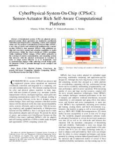
abstraction layer. However, it is not clear upfront, which fault type or error is most effectively tackled at what abstraction layer and by what form of countermeasure. Detecting and correcting an error directly at the level where it occurred may be possible but may not be the most efficient mean. For example, hardening SRAM cells against radiation-induced bit flips by means of using larger transistor comes at the expense of an area increase for each and every SRAM cell within the memory array. Applying information redundancy techniques in form of error detection and correction coding (ECC) during memory write/read operations results in much less area overhead and achieves the same result. To effectively tackle these challenges while not compromising with performance targets, the ability to model and evaluate the various faults and errors at and across all SoC abstraction layers is a necessity. It is the declared objective of the German Research Foundation (DFG) Priority Program SPP1500 ”Dependable Embedded Systems” to develop new cross-layer design methods and architectures for coping with reliability, performance degradation and increasing power dissipation issues when migrating to new CMOS technology nodes [1]. The proposed Resilience Articulation Point (RAP) method is the result of several working group meetings among SPP1500 partners and aims at provisioning a probabilistic error modeling and bottom-up error abstraction / transformation framework to characterize errors at different SoC hardware and software layers. II. R ESILIENCE A RTICULATION P OINT (RAP) M ODEL The RAP model is based on three principal pillars: First, the hypothesis that whatever physical phenomenon is the root cause for a fault, if it is not masked (i.e. eliminates itself), it will manifest as a permanent or transient singleor multi-bit signal invalidation Pbit (see Fig. 1). Second, cross-layer dependability optimization requires probabilistic methods for reliability modeling in order to cope with, abstract and quantify the impact of complex low-level fault exposures at higher levels. Third, transformation functions TL convert probabilistic error functions PL at abstraction level L into probabilistic error functions PL+i at level(s) L + i (i ≥ 1).
In graph theory, an articulation point is a vertex that connects sub-graphs in a biconnected graph, and whose removal would result in an increase of the number of connecting arcs within the graph. Translated to our domain of dependability challenges in SoC systems, spatially and temporally correlated bit flips represent the single connecting vertex between lower layer fault origins and the upper (hour glass) layer error and failure models of HW/SW system abstraction. Failure
Crash
„No effect“ Data corruption … Wrong branch decision Invalid CPU reg
Error
Bit Flip Faults
Jitter
Electromigration
Signal / Vdd noise
Physical sources
Radiation
Crosstalk
Coupling (C) Temperature Process variation
Fig. 1. Cross-layer representation of faults, errors, and failures with bit flip as Resilience Articulation Point
Error functions for different fault origins (radiation, aging, crosstalk or thermal hotspots, to name a few) and error transformation functions (such as for determining silent data corruption (SDC) or detected uncorrectable error (DUE) rates in microprocessor designs) are vital for the expressiveness of a RAP-based dependability assessment. However, it is not the intention of RAP (and beyond its abilities) to consider error and transformation functions to be an integral part of RAP. Neither is RAP a tool to develop such functions. RAP rather provides a framework where different fault origins, each being expressed as probabilistic bit errors for a particular signal, can be accumulated to represent an error function covering several physical shortcomings. Even when this accumulation and individual error models are approximate, they relief the SoC designer with expertise at higher abstraction levels from the details of the technological and device level aspects of SoC. This concept is applicable at each abstraction level including and above the bit or signal level. Cross-layer approaches are suggested in related work as feasible techniques to enhance reliability of complex systems ([2],[3]). RIIF [4] proposes a standard language to foster exchange of reliability information and models among components at different levels and different EDA tools. Fault and error modeling in the space and time domain has a long tradition in the LSI testing community. The generalized conditional line flip model [5] allows specification of Boolean and temporal activation conditions. Excessive process variations may cause test invalidation of delay tests which threatens product quality. Probabilistic fault modeling aims to quantify the quality of the test and final product w.r.t. the parameter space in spite of high uncertainty of variations [6]. The remainder of the paper is structured as follows: Section III introduces the basic assumptions of our probabilistic
error modeling under environmental, process and system state related constraints. A realistic SRAM circuit was used as example in section IV to calibrate the analytical model with real hardware for the fault scenario of radiation induced bit flips (soft errors). This is followed by a generalization of the SRAM fault model towards combinatorial and sequential logic circuits. Section V and VI describe how the RAP bit flip model is propagated towards higher abstraction levels up to the software application layer. III. T HE L OWER H ALF O F T HE H OUR G LASS The task of an error model at the lower levels is to describe the probability of an occurring bit error as a function of parameters that may change during system design or operation. We propose to model the error probability P of a bit by an error function F of three parameter vectors: Environmental and operating conditions E, design parameters D, and (error) state of correlated bits S. P = F(E, D, S)
(1)
This generic model has to be adapted to every circuit component and fault type independently. This enables then the modelling of different components (e. g. SRAM or latches) and different errors (e. g. soft errors or timing violations). A. Environmental and Operating Conditions E Almost all the functionality of a circuit is dependent on its environmental conditions. Device temperature and supply voltage values determine the electrical properties of all components in the circuit. Circuit age changes electrical properties such as threshold voltage. Other possible parameters include clock frequency or neutron flux density. These parameters represent an interface to either user decisions or other models in the design process. For example, in a simplified analysis supply voltage might be a fixed value, while in a more detailed analysis it might come from some more advanced model [7]. B. Design parameters D During the design stage several decisions have to be made. For example, shall arithmetic adders follow a ripple-carry or carry-lookahead architecture (enumerative decision)? What technology node to choose (discrete decision)? How much area should one SRAM cell occupy (continuous decision)? This allows the designer to make trade-offs between different decisions which all influence the error probability. C. Correlated (Error) States S To model the dependence of the error probability on location, circuit state, and time it might be necessary to include several state variables. These state variables lead to a model which is built from conditional probabilities P(b1 |b2 ), where the error probability of the bit b1 is dependent on the state of the bit b2 . For example, the failure probability of one SRAM cell depends on the error state of neighboring SRAM cells due to the probability of Multi Bit Upset (MCU) [8]. For an 8T
Internal node Q @ 1
WL
M 2 M 5
VDD
Q M1
5.5
Physics
M 4 Q
Induced charge distribution (Eq. 2 & 3)
M 6
M3
BL
Circuit level
6
45 32 22 16
nm nm nm nm
6T SRAM
Critical Charge (fC)
Device physics, Cosmic ray collision
Critical Charge (fC)
Technology/VDD
4
2
0.5
0.6
0.7
0.8
1
4.5 4 3.5 3
0
2
Supply Voltage (V)
Fig. 3.
4
6
8
Target Yield (σ)
(a) Dependence on VDD for different technologies
BL
Neg. current injection
0.9
8T SRAM - Node Q 8T SRAM - Node Q
5
(b) Dependence on target yield (in sigma) for different architectures
Critical Charge Dependence
Qcrit (Fig. 3)
with variable pulse height
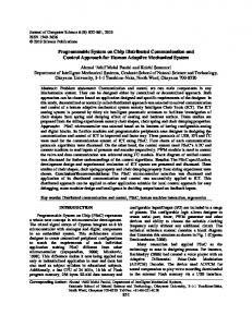
Calculation of Bit flip probability (Eq. 4) Fig. 2.
Architecture
SRAM Bit Flip Model
SRAM cell it also depends on the stored value of the SRAM cell as the bit flip probability of a stored one is different from a stored zero. D. The Error Function F The error function F finally takes the three parameter sets E, D, and S and returns the corresponding bit error probability. The error function is unique for a specific type of fault and for a specific circuit element. It might be possible to express the error function by simple analytical formulas. On the other hand, the error function might also require a nonclosed form representation, e.g. a timing analysis engine or a circuit simulator. IV. E XAMPLES FOR L OW-L AYER E RROR M ODELS In the following sections we describe bit flip error models of SRAMs and combinational or sequential logic cells. Similar methods were presented in [9]. A. SRAM Single Event Upsets One common example where bit flips are encountered in a chip is an SRAM cell. We will show in this example how neutron induced bit flips can be modeled in an SRAM array by using the generic model from Section III. A bit flip in an SRAM cell occurs when a particle strike induces enough charge on a point within the cell to cause a flip in the cell’s content. Thus, an SRAM bit flip model requires the critical charge to flip a cell as well a distribution describing the probability of charge injection (see Fig. 2). The critical charge which is required to flip a cell can be characterized for a given cell architecture using SPICE simulation [10]. Variation of environment temperature or cell supply voltage introduces a dependence of critical charge Qcrit on environmental conditions (Fig. 3a). The dependence on design parameters can also be characterized in a similar way, and the influence of cell area can be modeled by varying the size of the transistors inside the SRAM cell. The dependence on target yield can be found by adding a worst-case analysis
to the characterization as described in [11]. This results in a discrete model for the critical charge Qcrit dependent on environmental and design parameters (Fig. 3) which may additionally be approximated by some analytical function. For the second part of the model in Fig. 2 we need the probability that a charge which is larger than the critical charge is injected by a particle strike. The probability that a neutron strikes the cell can be modeled by a Poisson process [12]: (Φ · A · T )k (2) k! This equation expresses the probability that k neutrons hit an area A during the time interval T which is exposed to a neutron flux Φ. These neutrons are then uniformly distributed over the SRAM area and may only cause an error if they hit the critical area of one of the cells. Once the neutron strikes the critical area of the cell it may generate electron-hole pairs, which have the potential to change the charge stored on the capacitances inside the chip. We assume in the following that the probability distribution of injected charges due to a neutron strike follows an exponential distribution [13]: � � 1 Qinjected fQ (Qinjected ) = exp − (3) Qs Qs P (N (T ) = k) = exp (−Φ · A · T )
The parameter Qs is the charge collection slope due to one neutron strike, which is technology dependent [10]. The probability PSEU of a cell flip, and thus a bit error Pbit (~x, t), can then be composed from the critical charge of the cell Qcrit (Fig. 3) and equation 3: Z
∞
PSEU (Q ≥ Qcrit |Node Q = 1) =
fQ (Q)dQ
(4)
Qcrit
With increasing integration density the probability of Multi Bit Upsets increases. Possible reasons for this include the successive hit of multiple storage nodes by the same neutron, shared charge to adjacent cells, or parasitic bipolar transistors in the case of bulk technology [14]. To correctly account for Multi Bit Upsets we therefore have to add error state variables to the model. For this we first have to characterize the occurrence probability of given shapes [15]. Using these occurrence probabilities we can account for Multi Bit Upsets using conditional probabilities which determine the probability
that an adjacent cell is upset given the upset of spatially close cells [8]. B. Combinatorial and Sequential Logic When a neutron strikes a combinatorial or sequential logic block within the SoC, it will result in a charge separation within the semiconductor substrate material which may lead to a voltage pulse on a signal wire line (see signal A in Fig. 4). tp A
1
&
B
Y
C clk
C clk
T Hold
Bit flip as result of SEU or SET
The temporal width of the voltage pulse again depends on the energy of the particle, the technology feature size, the capacitive load of the signal, the supply voltage (in other words, on the E, D, and S parameters). However, the voltage pulse only results in a functional error (i.e. a false bit value latched into the following register stage affecting signal Y), if the pulse propagates from the location of occurrence to the register stage on a combinatorially sensitized path and overlaps with the critical time window ∆Tcrit = TSetup +THold around the active clock edge. Otherwise, the pulse will be masked out and thus, never be noticed. The probability for a bit error Pbit (~x, t) within sequential logic again is spatially (where in the combinatorial net did the strike occur) and temporally (what is the combinatorial path delay between strike location and register input) correlated with the fault and, with the probability Psense to have a sensitized path to the register, approximated as: Pbit (~x, t) ≈
(1 − Pbit (xi , t)) (6)
xi ∈~ x
T Setup Fig. 4.
Y
Pword (~x, t) = Tbit ◦ Pbit (~x, t) = 1 −
TSetup + THold + tp · Psense · PSET Tclk
(5)
Signal Y in Fig. 4 can be considered as an individual bit of a data word in a sequential data path pipeline or a bit within a state vector of a control FSM. Upsets on clock trees would result in multiple (hundreds of) erroneous register contents (data / control word corruptions). Clock tree upsets can be modeled as transient bit flips too, but will occur significantly less likely as clock buffers are usually hardened by multiple sequential nMOS and pMOS transistors in the buffer / inverter designs. A signal degradation on an i/o bit will result in an interface (control) error at a higher layer of abstraction and is also in line with the RAP model. In consequence, we now have a probabilistic bit flip model for combinatorial and sequential logic, interconnect wires, external interfaces and memory arrays, and thus cover all fundamental functional building blocks of SoCs or computing architectures.
The derivation of word error probabilities under consideration of correlated data bits and interleaving is also possible. We refer to [16] for a more complete discussion of this more complex case. When operand variables of arithmetic operations are stored in an SRAM memory array, then Pword (~x, t) describes the probability with which these variables contain erroneous data. In case the same variables are kept in the CPU register file, then a different Pword (~x, t) describes the trustworthiness of the contents of the register file. The two Pword (~x, t) probabilities are different because the technological (D) and state-related constraints (S) of SRAM arrays and a register files are different. Pword (~x, t) can also incorporate potential dependability countermeasures applied at word level abstraction layers (e. g. ECC detecting and correcting up to k bit errors per word). In case of ECC protection, only N > k accumulated bit errors within one and the same data word and between two consecutive write refreshes will result in a word / variable error. N < k bit flips per data word remain invisible (i.e., are masked) for the software layer. Hence, an ECC protected memory has a different Pword (~x, t) than a non-protected memory, although both may have the same bit level Pbit (~x, t). System SW Levels
B
Process Data Architecture
System HW Levels
A
V. T HE U PPER H ALF OF THE H OUR G LASS Bits or individual signals are meaningful targets for describing errors at the transistor, logic gate and RTL levels of abstraction. At higher layers, compounds of multiple signals/bits, referred to as data, control or address words, FSM state vectors, variables, interfaces or data structures, are more intuitive and descriptive, particularly for software developers (see Fig. 5). On the other hand, a memory data word is nothing but a bundle of multiple (say 32) consecutive memory cells or memory bits. Thus, when assuming individual bit errors Pbit (~x, t) in space ~x and time t within memory cells to be independent, one can determine the approximate Pword (~x, t) error probability by the following concrete transformation function Tbit :
Macro
Driver
Tasks OpCode
Data
I/O Memory HWCore Accel. Bus
Pipeline
Address Arbiter Decoder B2
B1
A2
&
=1
B0