Indian Journal of Pure & Applied Physics Vol. 45, September 2007, pp. 767-769
Current-mode multifunction filter using current differencing transconductance amplifier N A Shah, Munazah Quadri & S Z Iqbal Department of Electronics and Instrumentation Technology, University of Kashmir, Srinagar 190 006 E-mail:
[email protected] Received 3 April 2007; accepted 5 July 2007 This paper presents a novel current-mode (CM) second-order filtering configuration capable of realizing two filtering functions simultaneously. The circuit employs a single current differencing transconductance amplifier (CDTA), two capacitors and a resistor. The circuit can realize highpass (HP) and bandpass (BP) filtering responses simultaneously and bandpass (BP) and lowpass (LP) responses through RC:CR transformation. All active and passive sensitivities are low. PSPICE simulation results are included. Keywords: Current-mode filters, Current differencing transconductance amplifier, Analog signal processing IPC Code: H01S
1 Introduciton The present trend of research activities is towards the development of continuous-time CM circuits as these offers several potential advantages such as simplicity of signal operations, higher frequency operation and wider dynamic range as compared with their voltage-mode (VM) counterparts1-5. The CM filters employing different active building blocks such as operational amplifier (OA), operational transconductance amplifier (OTA), current conveyor (CC), and four terminal floating nullor (FTFN) have been developed3-5. Current differencing transconductance amplifier (CDTA), a recently introduced active device having two current inputs, current outputs and having the electronic tunability through its transconductance gain seems to be highly desirable active device for the implementation of signal processing in current-mode6,7. With this element, it is possible to obtain filter circuits with lesser number of passive components vis-à-vis its counterparts and in some applications it can lead to compact structures8. Some realizations using CDTA as active element operating in CM have been developed7-10. In this paper, a new biquad circuit having a single input and two outputs with one output always at high impedance is presented. The circuit employs bare minimum number of active and passive components i.e. one CDTA, two capacitors and a resistor. The circuit is capable of realizing two filtering signals simultaneously depending on the nature of the admittances.
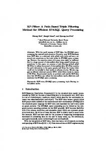
The gain of responses available at the output terminal of CDTA can be tuned electronically and independently of the filtering parameters. The sensitivity figures are low. 2 Circuit Description Fig. 1 shows the behavioural model and schematic symbol of CDTA. The inputs p and n produce a difference current which is transferred to the z terminal and the voltage at the z terminal is converted into a set of output currents by a dual output transconductance stage. The port relationships characterizing CDTA are given by: Vp = Vn = 0, Iz = Ip – In, Ix = ± gVz The current-mode filter topology is shown in Fig. 2. The analysis of the circuit yields the following transfer function: Io1 g1Y 1 = Iin (Y1 + Y2 ) (Y3 + g2 )
… (1)
Fig. 1— (a) Behavioural model, (b) symbol of CDTA element
INDIAN J PURE & APPL PHYS, VOL 45, SEPTEMBER 2007
768
I o1 = I in
I o2 = I in
For Y1=sC1, Y2=
… (2)
1 and Y3= sC2, the transfer function R1
becomes I o1 = I in
I o2 = I in
g s 1 C2
1 g g2 s + s + 2+ C1 R1 C 2 C1C 2 R1 s2 1 g g2 s + s + 2+ C1 R1 C 2 C1C 2 R1
… (3)
Q
=
1 g g2 s + s + 2+ C1 R1 C 2 C1C 2 R1
… (4)
g2 C1C 2 R1 C 2 + g 2 C1 R1 C1C 2 R1
Also the gain of BP response is given by H BP =
… (6)
g2 C1C 2 R1
ωo = ωo Q
=
C 2 + g 2 C1 R1 C1C 2 R1
The gain of LP and BP responses are given by: g H LP = 1 g2 H BP =
2
ωo =
… (5)
2
2
The expressions for pole frequency ωo and bandwidth ωo/Q are given by:
ωo
1 g g2 s + s + 2+ C1 R1 C 2 C1C 2 R1 1 s C1 R1 2
The expressions for pole frequency ωo and bandwidth ωo/Q are given by:
Fig. 2—Proposed CM filter
Io 2 YY 1 3 = Iin (Y1 + Y2 ) (Y3 + g2 )
g1 g2 g 2 C1C 2 R1
g1C1 R1 C 2 + g 2 C1 R1
As it is clear from Eq. (4) that the gain of the BP response can be electronically tuned by g1 independently of the pole frequency and bandwidth. 1 Now, after interchanging R1 and C1 i.e. for Y1= , R1 Y2= sC1 and Y3= sC2, Eqs (1) and (2) yield:
C2 C 2 + g 2 C1 R1
Thus, the gain of LP response is electronically tunable through the transconductance gain g1 independently of pole frequency and bandwidth. 2.1 Sensitivity
The active and the passive sensitivities are: S gω2o = − S Cω1o = − S Cω2o = − S Rω1o = ωo
S gQ2 = ωo
S CQ2 = ωo
S CQ1 = ωo
S RQ1 =
g 2 C1 R1 C 2 + g 2 C1 R1 − g 2 C1 R1 C 2 + g 2 C1 R1 − C2 C 2 + g 2 C1 R1 − C2 C 2 + g 2 C1 R1
which are all less than 1.
1 2
SHAH et al.: CURRENT-MODE MULTIFUNCTION FILTER USING CDTA
769
tations given in Fig.3. The simulated responses are shown in Fig. 4.
Fig. 3—Implementation of CDTA by (a) CCII+, (b) CDBA and (c) CFA, all with OTAs
3 Conclusion In this paper, a new CM filtering configuration based on and employing a single CDTA and only three passive components i.e. two capacitors and a resistor is presented. The circuit is capable of realizing two responses viz. highpass and bandpass simultaneously. Through RC:CR transformation, the circuit can also realize lowpass and bandpass responses simultaneously. The active and passive sensitivities are all less than one in magnitude. PSPICE simulation results confirm the theoretical analysis. References
Fig. 4—Simulated results of the proposed filter 2.2 Simulation results
The performance of the proposed filter was verified using the PSPICE simulation program. The values of the passive components were chosen as R1=1 kΩ, C1= C2=1 nF and the value of transconductance g was taken as 1 mS for a pole frequency of 159 kHz. The CDTA can be implemented using the CMOS given by Uygur and Kuntman11 or by the any of the implemen-
1 Wilson B, IEE Proc G, 137 (1990) 63. 2 Ramirez-Angulo J & Sanchez-Sinencio E, IEEE Trans Circuits Systems- II, 39 (1992) 337. 3 Hou C L, Huang C C, Lan Y S, Shaw J J & Chang C M, Int J Electronics, 86 (1999) 929. 4 Liu S I & Lee J L, Electron Lett, 32 (1996) 1079. 5 Wu J & El-Masry E I, Int J Electronics, 85 (1998) 553. 6 Biolek D, ECCTD’03, Krakow, Poland, (2003) 397. 7 Biolek D & Gubek T, Internet journal Elektrorevue, www.elektrorevue.cz. 8 Uygur A, Kuntman H & Zeki A, Proc of ELECO 2005: The 4th International Conference on Electrical and Electronics, Bursa, Turkey, (2005) 46. 9 Bekri A T & Anday F, In proceedings of the 2005 European Conference on Circuit Theory and Design, Cork Ireland, 2 (2005) 93. 10 Biolek D & Biolkova, CSCC2003, Corfu, Greece, (2003) 8. 11 Uygur A & Kuntman H, IEEE MELECON 2006, May 16-19, Benalmadena (Malaga), Spain, (2006) 23.