Department of Electrical Engineering - Systems. University of ... evolved as cost-e ective techniques for testing digital circuits. ... cuit that requires minimal BIST area overhead and that ... Given a scheduled data ow graph we allocate opera-.
Data Path Allocation for Synthesizing RTL Designs with Low BIST � Area Overhead Ishwar Parulkar, Sandeep Gupta and Melvin A. Breuer Department of Electrical Engineering - Systems University of Southern California Los Angeles, CA 90089-2562.
Abstract|Built-in self-test (BIST) techniques have evolved as cost-e�ective techniques for testing digital circuits. These techniques add test circuitry to the chip such that the chip has the capability to test itself. A prime concern in using BIST is the area overhead due to the modi cation of normal registers to be test registers. This paper presents data path allocation algorithms that 1) maximize the sharing of test registers resulting in a fewer number of registers being modi ed for BIST, and 2) minimize the number of CBILBO registers. I. Introduction
Built-in self-test (BIST) techniques have gained acceptance for testing complex digital designs. These techniques involve modi cation of the hardware on the chip such that the chip has the capability to test itself. One of the considerations in BIST techniques is the extra area needed for the test circuitry. How to reduce the BIST area overhead without sacri cing the quality of the test is an important research problem [1]. Considering testability at an earlier stage in a design can lead to a more e�cient exploration of the design space, thus resulting in a circuit that requires minimal BIST area overhead and that meets area, throughput and other requirements. The eld of high-level synthesis has made signi cant progress in addressing area-performance requirements. However investigation of synthesis methods that take into account testability has only recently received attention from the research community [2],[3],[4]. The objective of these methods is ease of test generation and e�cient partial scan. For designs that support BIST, Avra proposed a register allocation method that minimizes the number of self-adjacent registers in the design [5]. The assumption in this work is that every self-adjacent register needs to be modi ed to be a CBILBO register, and thus the overhead is high. Papachristou et al. rst presented a combined register and ALU allocation method that generates self-testable designs that do not have any self-loops [6]. The approach
is based on constraining the allocation to generate a selftestable template which is very restrictive and hence results in exploring a small subspace of the testable design space. Later they presented a method of generating selftestable designs by extending the self-testable template to include one speci c con guration of a self-adjacent register [7]. This approach is still restrictive because it does not consider many other self-adjacency scenarios that do not require CBILBOs and is based on synthesizing templates by simultaneous constrained allocation of ALUs, registers and interconnect. Given a scheduled data ow graph we allocate operations, variables and data transfers such that the functional constraints are satis ed and the area overhead required for BIST is minimal. The BIST methodology used is based on the concept of an I-path [8] and the sharing of I-paths between modules. We show that self-adjacency does not necessarily imply poor testability and have derived exact conditions of register assignment which necessitate CBILBOs. Our model subsumes the testability design styles considered in [5] and [7]. The conditions derived and the separate assignment of operations, variables and data transfers enables an e�cient exploration of a larger testable design solution space. II. Test methodology
The allocation scheme presented in this paper is directed towards synthesizing data paths that are to be tested using a partial intrusion pseudo-random BIST methodology. In this methodology, some of the registers in the data path are recon gured to support test pattern generation (TPG) and signature analysis (SA) during the test mode. A built-in logic-block observation (BILBO) register is a design capable of these modes. The basic BILBO BIST architecture consists of partitioning a circuit into a set of registers and combinational blocks. For complete testing of all the combinational blocks in the design, di�erent mappings of registers to TPGs and SAs is required. The concept of an I-path can be used e�ectively to explore the various mappings [8]. The data path � This work was supported by the Advanced Research Projects architectures comprising registers and combinational opAgency and monitored by the Federal Bureau of Investigation under erator modules with the multiplexer connectivity model Contract No. JFBI90092. lend themselves naturally to the concept of I-paths and the BILBO BIST methodology. Also the mapping of reg32nd ACM/IEEE Design Automation Conference Permission to copy without fee all or part of this material is granted, provided isters to TPGs and SAs is independent of the function that the copies are not made or distributed for direct commercial advantage, and the gate-level implementation of the operator modthe ACM copyright notice and the title of the publication and its date appear, ules. Hence the testability constraints for this BILBO and notice is given that copying is by permission of the Association for BIST methodology are appropriate for consideration durComputing Machinery. To copy otherwise, or to republish, requires a fee and/or specific permission. 1995 ACM 0-89791-756-1/95/0006 $3.50 ing high-level synthesis.
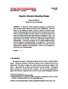
R1
a
R3
R2
b
0
c1
0
+1
1
1
c d
m1 L
e
+2
R
M1
*1
2
g
f
O
*2 0 1
R4
m2
h
c2
R5
Fig. 1. A generic con guration with simple I-paths
De nition 1: (Abadir and Breuer [8]) An identity path, I-path is a data path from a primary input or a register
to an input port of an operator module or from an output port of an operator module to a primary output or a register so that data can be transferred unaltered. The rst and the last elements of an I-path are called the head and tail, respectively, of the I-path. A simple I-path is an I-path consisting of at most one register and no operator modules. An example of a binary operator module M1 and simple I-paths to and from its ports is shown in Fig. 1. Input port R has a simple I-path from R3 . This I-path is active at all times and is the only I-path to port R. Input port L has simple I-paths from R1 and R2 that pass through multiplexer m1 . I-paths with multiplexers can be activated by appropriate control signals, for example c1 in this case. A con guration of I-paths that covers all the ports of a module is called a BIST embedding of the module. The heads of the I-paths to the input ports are modi ed as TPGs and the tails of the I-paths from the output ports are modi ed as SAs. If the con guration chosen is such that a head and a tail are the same register then that register has to act as a TPG and SA at the same time. To ensure high fault-coverage a concurrent built-in logic block observation (CBILBO) register is required [9]. Generally, there is more than one embedding for a module. The choice of TPGs and SAs for testing this module largely depends on how and which registers are connected to the rest of the modules. For minimizing the BIST area overhead, the design is analyzed globally to determine the test resource allocation such that all operator modules are tested with a minimal number of registers modi ed as test resources. Also a CBILBO register has an area approximately twice that of a normal register and hence another objective is to minimize the number of CBILBOs. Since minimal area overhead is our objective, it is not necessary to test all the combinational modules at the same time, i.e. in one test session. The assignment of registers and interconnect presented in this paper is done with the aim of maximizing sharing of I-paths between di�erent modules. Also the assignment procedure takes into account the possibility of requiring CBILBO registers in the testable design and avoids such assignments. This leads to superior results compared to existing synthesis procedures. III. Module and register assignment
The behavioral description is assumed to be given in the form of a data ow graph (DFG) G = (V; E) where
3 4
Fig. 2. A scheduled DFG V is the set of operations and E is the set of variables (operands and results of the operations) and a schedule S : V ! f 1, 2, 3,... g where S(v) corresponds to the control step in which operation v is scheduled. All operators are assumed to be binary and commutative. Noncommutative operators can be handled by adding additional constraints in our assignment procedures. Unary operators can be treated as a special case of binary operators. The assignment is performed in the following order module assignment, register assignment and nally interconnect assignment. We chose the above order for the following reasons. The module assignment space is relatively much smaller than the other spaces and the impact of module assignment on the functional area is large. Hence there is little exibility within the module assignment solution space for improving testability. Most of the
exibility for minimizing test resources for BIST exists in register assignment. Also, registers can be viewed as potential test resources only after the module assignment is xed. Interconnect assignment is strongly related to module and register assignment and its e�ect on functional area can be implicitly considered during those phases. In our approach, the interconnect assignment that follows register assignment tries to make the best use of the register assignment to further reduce BIST overhead. Module assignment is done without any testability consideration. Existing algorithms that optimize area are used. The module assignment is de ned as � : V ! M where M is the set of available modules. The subset of V mapped onto module Mi will be referred to as Vi . Each operation v 2 Vi will be referred to as an instance of Mi . De nition 2: The temporal multiplicity of module Mi , TM(Mi ) is the number of operations from V mapped onto Mi , i.e. TM(Mi ) =j Vi j. Consider the scheduled DFG shown in Fig. 2 and the following module assignment. Operations +1 and +2 are assigned to module M1 and operations �1 and �2 are assigned to module M2 . Thus V1 =f +1 ; +2 g where each element is an instance of M1 and TM(M1 ) = 2. De nition 3: The input variable set of module Mi , IM is the set of all the operand variables associated with each instance j of module Mi . The output variable set of module Mi , OM is the set of all the output variables associated with each instance j of module Mi . For the scheduled DFG of Fig. 2 and the above mentioned module assignment IM1 = f a; b; c; d g and OM1 = f d; f g. A register assignment �R can be de ned as a partition f R1 ; R2; :::; Rr g of the set of variables E such that for any i
i
two variables u and v in Rk , 1 � k � r, their lifetimes do not overlap. For the scheduled DFG of Fig. 2, a minimum of three registers are required. There are 108 distinct assignments of the variables in E to three registers. With respect to register and functional unit area these 108 assignments are equivalent. Only a subset of these result in more testable data paths (low BIST overhead) than the rest. Our algorithms direct register assignment to this low BIST area overhead subset of the solution space. A. Maximizing sharing of test resources
a
b
R1
R2
R3
R4
R5
y
a, x
b
p
q
op1 c
• • •
p
q op2
y
x
• • •
M2 = (op1, op2)
M1 = (op3)
r
op3 z z, c
Observation 1: Given a module assignment, (a) An assignment of variables to a register Ri such that Ri \ IM = 6 � and Ri \ IM 6= �, guarantees the creation
(a)
R6
(b)
Fig. 3. Sharing of I-paths The sharing degree of a register R is of simple I-paths to an input port of module Mj and to De nitionP5: an input port of module Mk that share a common head, SD(R) = mj=1(XjR + YjR ), where namely register Ri, independent of the subsequent inter_ X v and Y R = _ Y v connect assignment. XjR = j j j (b) An assignment of variables to a register Ri such that 8v2R 8v2R Ri \ OM 6= � and Ri \ OM 6= �, guarantees the creation of simple I-paths from the output port of module Mj and sharing degree of a register is thus the total number from the output port of module Mk that share a common of The input variable sets and distinct output variable tail, namely register Ri, independent of the subsequent setsdistinct that contain at least one element of R. The sharing interconnect assignment. degree re ects the number of modules for which the regact as a TPG and the number of modules for Fig. 3 shows the formation of the simple I-paths with ister can it can act as a SA. Consider a register R that has a common head and with a common tail. Consider a which assigned some variables. Let the sharing degree of portion of a scheduled DFG shown in Fig. 3(a). Each of been R after another variable v is assigned to it be P denoted by the operations are scheduled in a di�erent control step SD(R; v). Now SD(R; v) = SD(R)+SD(v) mj=1(XjR � and all the variables depicted have disjoint lifetimes. Let op3 be one of the operations assigned to module M1 and Xjv + YjR � Yjv ). Using this measure the assignment prooperations op1 and op2 be the only operators assigned to cess can be guided by choosing merges that result in large module M2 . Now IM2 = f a; b; p; q g and IM1 = f x; y; ::: g. increases in the sharing degrees of registers. The increase IM1 could have elements in addition to x and y depending in the sharing degree of a register R as a result of assignon which other operations are assigned to M1 . Suppose ing variable v to it will be denoted by �SDv (R). (i.e. each of the input variables of M2 is assigned to a separate �SDv (R) = SD(R; v) SD(R)). register, e.g., a to R2, b to R3, p to R4 and q to R5. Now The register assignment problem can be modeled as if a variable from IM1 , say x, is assigned to one of these coloring of the variable con ict graph. A variable conregisters, say R2, a simple I-path is created from R2 to an ict graph has vertices corresponding to variables with input port of M1 also. This is shown in Fig. 3(b). The an edge between variables only if they have overlaponly requirement for M1 and M2 to have I-paths with a ping lifetimes. A two coloring of this graph corresponds to a common head is that at least one variable each from IM1 valid register assignment with each color corresponding to and IM2 be assigned to the same register, i.e. there should a register. In the rest of the paper use the terms be a register Ri such that Ri \ IM1 6= � and Ri \ IM2 6= �. color and register interchangeably. Ifwethewilldata graph Similarly if at least one variable each from OM1 and OM2 description does not contain mutual exclusion ow constructs is assigned to the same register, R6 in this case, I-paths and loops, the resulting variable con ict graph is an interfrom the outputs of both the modules to R6 are created. val graph [10]. A minimum coloring of these graphs can In Fig. 3(b), the register R2 can be used as a TPG for obtained in polynomial time [11]. The minimum colorboth the modules and the register R6 can be used as a be ing algorithm on interval graphs is a greedy algorithm and SA for both the modules by activating the appropriate I- at every it has a restricted choice of variables which paths. Thus for maximizing the sharing of TPGs between does not step allow an e�cient exploration of the solution the input ports of modules an assignment �R is desirable space to search for for a good testability solution. such that for each Ri the number of input variable sets The greedy coloring uses the hereditary propwith which it has at least one variable in common is max- erty of interval graphs algorithm which is de ned through simplicial imized. Similarly the number of output variable sets with vertices. A vertex v of a graph G is simplicial if its adwhich each Ri has at least one common variable should jacency set induces a clique in G. The adjacency set is be maximized. the set of all vertices that are connected to v. An intergraph has at least two simplicial vertices. If a simDe nition 4: The sharing degree SD(v) of a variable val v is the sum of the number of modules for which v is an plicial vertex and all its incident edges are removed, the input variable and the number of modules for which v is remaining graph is also an interval graph. An ordering of the vertices such that each vertex is a simplicial vertex an output variable.v If v 2 IM , let Xj = 1, else Xjv = 0;Pif v 2 OM , let of the remaining graph is called a perfect vertex eliminascheme (PVES). An interval graph has many such Yjv = 1, else Yjv = 0. Then SD(v) = mj=1 (Xjv + Yjv ), tion perfect vertex elimination schemes. The optimal colorwhere m is the total number of modules assigned. ing algorithm constructs one such scheme arbitrarily and j
k
j
k
j
j
colors the vertices greedily in the reverse order (reverse PVES) [11]. Our heuristic is di�erent from the optimal coloring algorithm in two respects: 1) it selects the PV ES in a more structured way taking into account information such as the sharing degree of variables and size of maximal cliques; and 2) the vertices are then colored using this scheme, but instead of assigning colors greedily, many more coloring possibilities are explored and the one most suited for maximizing the sharing of test resources for BIST is selected. 1. Selection of a PV ES: With each vertex of the con ict graph we associate a sharing degree as per De nition 4. In addition we also nd the size of the maximum clique to which each vertex belongs. The size of such a clique indicates the number of registers to which this variable cannot be assigned. Let MCS(v) denote the size of such a clique containing v. The vertices are ordered such that if v is before w, then SD(v) � SD(w) and if SD(v) = SD(w) then MCS(v) � MCS(w). At every step of constructing a PV ES there is a choice of simplicial vertices. The PVES is now determined such that at each step a simplicial vertex that is earliest in this order is selected. Since vertices are colored in the reverse PVES order, this results in vertices with higher sharing degrees to be considered earlier when there is maximum exibility in the assignment of colors. Also since vertices with a higher MCS value are considered earlier more colors are xed in the earlier stages thus creating more coloring options to explore. This enables the heuristic to search the design space more e�ciently for nding a coloring with low testability area overhead keeping the number of colors close to optimum. 2. Coloring in reverse PV ES order: For the purposes of the following discussion the vertices will be referred to by their number in the reverse PV ES. Let the assignment after the kth vertex is colored be denoted as � :::; Rkc ) where Rki \ Rkj = � if i 6= j and SkRci=1=R(Rki =k1 ;fR1,k2;2,...,k g. The total number of registers after the kth vertex is colored is ck . The vertex (k+1) is assigned in the following way. If (k+1) con icts with all registers Rk1 ; Rk2 ; :::; Rkc then a new register Rkc +1+1 = fk+1g is created. Otherwise, out of the registers that do not con ict with (k+1) pick a register Rki such that �SDk+1 (Rki ) = SD(Rki ; k+1) SD(Rki ) is maximum. Such an Rki corresponds to a register that can best utilize (k+1) to improve its sharing as a test resource. If there is more than one such register then the tie is broken by considering the sharing degree of the registers and the one which has the higher sharing degree is chosen. Further ties are broken by taking into consideration the e�ect of the assignment on interconnect cost. There are two cases in which a register other than Rki might be preferable for assignment. Case 1: Consider the following example with 3 modules M1 , M2 and M3 with output variable sets OM1 = fa; bg, OM2 = fc; dg and OM3 = fe; f g. Assume that the assignment so far is R1 = fa; b; cg and R2 = fd; eg and f is the vertex under consideration for coloring next. Furthermore let us assume that f does not con ict with any of the other variables so it can be assigned to either R1 or R2 and assume �SDf (R1) > �SDf (R2). This implies that R1 can make the best use of variable f in terms of increasing its potential as a test resource. The increase in its sharing potential is due to the fact that since f 2 OM3 , k
k
k
k
•
a
•
b
•
•
c
•
e
•
•
f
g
•
h
d
Variables Sharing degree
v
:
a
b
c
d
e
f
g
h
SD(v)
:
1
1
2
2
1
2
2
1
:
2
2
3
3
3
2
2
1
Max. clique size MCS(v)
Fig. 4. Con ict graph of variables R1 can be a potential SA for testing module M3 . But register R2 already has variable e assigned to it and e 2 OM3 . If SD(R2 ) � SD(R1 ; f), there is a greater likelihood of R2 being chosen as a test resource in which case it can act as a SA for module M3 . Assigning f to R1 in such a case would only increase the interconnection cost since module M3 would have to transfer data from its output to two registers instead of one. Hence if vertex (k+1) is an output variable of module Mj and if there is a register Rkl with which (k+1) does not con ict such that Rkl already has an output variable of Mj assigned to it then the nal sharing degrees of Rki and Rkl are compared. If SD(Rkl ) > SD(Rki ; k + 1) then (k+1) is assigned to Rkl instead of Rki even if �SDf (Rki ) is greater. Case 2: This case is analogous to case 1 above except that it deals with the possibility of selection of registers as potential TPGs. Since operators are binary, kthis casek requires the existence of two such registers, Rm and Rn . In general both the cases can arise in which case a set of candidate registers is created of all such registers Rkl , Rkm and Rkn and (k+1) is assigned to the one which results in the highest increase in its sharing degree. Again ties are broken so as to minimize interconnect. The optimality in the minimum coloring algorithm is guaranteed by assigning the vertex (k+1) to the rst Rki with which it does not con ict. Since our heuristic does not make such an assignment we cannot guarantee optimality in terms of the number of registers allocated. However the heuristic is near-optimal since it still relies on a PV ES of a con ict graph. In all the examples considered it resulted in the minimum number of registers. The details of the register assignment algorithm and the pseudo-code can be found in [12]. Consider the scheduled DFG in Fig. 2 with the following module assignment: M1 =f+1 ; +2g and M2 =f�1 ; �2g. The variable con ict graph along with the SD and MCS values is shown in Fig. 4. A perfect vertex elimination scheme of this graph satisfying the SD and MCS ordering is h; b; a; e; g; f; d; c. The coloring is now done in the reverse order, namely, c; d; f; g; e; a; b;h. The rst two vertices c and d are assigned to separate registers since they con ict and thus we have R21 = fcg, R22 = fdg and SD(R21 ) = 2, SD(R22 ) = 2. Considerf the2 assignment of the third vertex, f. Since �SD (R1) = SD(R21 ; f) SD(R21 ) = 4 2 = 2 which is greater than �SDf (R22 ) = SD(R22 ; f) SD(R22 ) = 3 2 = 1, f is assigned to R21 and we have �3R =(fc; f g, fdg). Vertex g is assigned the same color as d. Vertex e con icts with both the allocated registers and hence a new register is allocated and e is assigned to it. The sixth vertex, a,5 belongs to IM1 = fa; b; c; dg. There are two registers R1 =fc; f g and R52 = fd; gg that have elements from IM1 and sharing degrees 3 and 4, respectively. The increase in the
•
R1
•
R3
R2
R1
R2
R3
• •
•
M1
M2
TPG
M2
M1
(a)
(b) SA
TPG/SA
Fig. 5. Data paths from DFG in Fig.2. sharing degree of R53 due to a, �SDa (R53 ) is greater than �SDa (R51 ) and �SDa (R52 ). But the actual sharing degree SD(R53 ; a) is less than SD(R51 ) and SD(R52 ). Hence we prefer to assign a to R51 or R52 . R51 is chosen because of lower interconnect7 cost. The last vertex h increases the sharing degree of R1 and R73 by 1. However R72 has an element of OM2 to which h also belongs and SD(R72 ) is greater than SD(R71 ; h) and SD(R73 ; h). Hence h is assigned to R72 . The nal assignment is �8R = (fc; f; ag, fd; g; b; hg, feg). The data path corresponding to this register assignment and the given module assignment is shown in Fig. 5(a). The data path corresponding to a minimum coloring obtained without regard for testability is shown in Fig. 5(b). In both cases minimum interconnect was assigned after register assignment. It can be seen that in Fig. 5(a) R1 and R2 can be shared as TPGs between both the modules and R2 can be shared as a SA. So a minimal area BIST solution would be to convert R1 to a TPG and R2 to a CBILBO. Compare this to Fig. 5(b) where R2 is the only common TPG. Also the two modules do not have a SA in common. A minimal area BIST solution for this data path is R1 as a TPG and R2 and R3 as CBILBOs which is more costly than the minimal area BIST solution for the earlier design. B. Minimizing CBILBOs
Sharing test resources between modules is not su�cient to minimize the BIST area overhead because it could still result in the formation of data paths that require CBILBOs to test some modules. In a globally minimal BIST area overhead solution, a register might be modi ed into a CBILBO register even though it is not necessary to do so. However a situation where modifying a register to a CBILBO is absolutely necessary is the one which results in high BIST area overhead. In this section we derive the exact conditions for register assignment which when followed by minimum interconnect assignment necessitate the modi cation of a register to a CBILBO. De nition 6: An input register of module Mk is a register Ri such that at least one input variable (operand) of Mk is assigned to it, i.e. Ri \ IM 6= �. An output register of module Mk is a register Ri such that at least one output variable of Mk is assigned to it, i.e. Ri \ OM 6= �. The set of input registers and output registers will be denoted by IRk and ORk respectively. If a BIST embedding for a module is chosen such that the I-path from the output port of the module and the I-path to an input port of the module have the same register, a CBILBO has to be used. In general any register that is an input register as well as an output register of a module can be made a CBILBO in order to test the k
k
module. But it is essential for a register to be made a CBILBO only if it is a CBILBO in all the possible embeddings of a module. The conditions derived below are for a register to be a CBILBO in all possible BIST embeddings of the nal data path. Lemma 1: If all the possible BIST embeddings of module Mk require a CBILBO register then j ORk j� 2. From the above lemma and the de nition of an output register, if register Ri has to be a CBILBO in any BIST embedding of module Mk then either (i) Ri \ OM = OM , or (ii) Ri \ OM � OM and there exists a register Rj such that (Ri \ OM ) [ (Rj \ OM ) = OM . That is, the variables of the output variable set of Mk are assigned to either one or two registers. This information reduces the number of cases to be considered for deriving the exact assignment conditions for a register to be made a CBILBO. Lemma 2: A register Rx is a CBILBO in all embeddings of module Mk if and only if one of the following cases is true. Case(i): Rx \ OM = OM and Rx \ IMj 6= � for j = 1, 2, ..., TM(Mk ). Case(ii): Rx \ OM � OM and Rx \ IMj 6= � for j = 1, 2, ..., TM(Mk ) and 9 a register Ry such that (Rx \ OM ) [ (Ry \ OM ) = OM and Ry \ IMj 6= � for j = 1, 2, ..., TM(Mk ). Case(ii) is symmetrical in Rx and Ry and so either of them can be made CBILBO. The proofs of Lemma 1 and Lemma 2 are provided in [12]. Lemma 2 enables us to check if a particular assignment would result in a CBILBO in the BIST version of the design. The register assignment algorithm is modi ed to include the check and to avoid assignments leading to CBILBOs. If such an assignment cannot be avoided without allocating an extra register, we allow the assignment. Our experiments indicated that the assignment space is large enough for this situation to occur infrequently. k
k
k
k
k
k
k
k
k
k
k
k
k
k
k
k
IV. Interconnect assignment
k
Register assignment is followed by minimum interconnect assignment. For a given module assignment di�erent register assignments have di�erent e�ects on interconnect area. Our register assignment algorithm does not take into account the e�ect on interconnect area except to resolve ties. The typical situations that occur when two variables or intermediate registers are merged into one register are shown in Fig. 6. The corresponding increase or decrease in multiplexers and BIST resources as a result of the merges is also shown. Case 1: Merging variables/intermediate registers that have di�erent source modules and di�erent destination modules.(Fig. 6(a)) Case 2:Merging variables/intermediate registers where a source module of one variable is the destination module of the other variable.(Fig. 6(b)) Case 3:Merging variables/intermediate registers having only one destination module in common but di�erent source modules.(Fig. 6(c)) Case 4:Merging variables/intermediate registers having only one source module in common but di�erent destination modules.(Fig. 6(d))
TABLE I Design comparisons with BIST area overhead DFG Module Traditional HLS Testable HLS % Reduction in Assignment # Reg # Mux % BIST area # Reg # Mux % BIST area BIST area ex1 1+, 1* 3 3 18.14 3 3 10.67 30.00 ex2 1/, 2*, 2+, 1& 5 5 11.17 5 4 7.56 32.31 Tseng1 2+, 1*, 1-, 1&, 1j, 1/ 5 9 17.65 5 7 11.34 35.75 Tseng2 1+, 3 ALUs 5 7 10.04 5 10 5.66 46.62 Paulin 1+, 2*, 14 6 16.34 4 6 9.34 42.84
(a)
M1
M3
v1
v2
(c)
M3 +1 MUX -1 TPG/SA
v1,v2 M4
M2
(b)
M1
M1
M2
v1
v2
M2
M4
M1 v1,v2
M2
M3
M2
M1
M2
M1
v1
v2
M3
M2 0 MUX 0 TPG -1 SA
v1,v2 M3
M3
M1
(d)
M1
v1
v2
M2
M3
M1
(e)
v1
M2
+1 MUX -2 TPG/SA +1 CBILBO
0 MUX -1 TPG 0 SA
v1,v2 M2
M3
M1 v2
v1,v2
-1 MUX 0 TPG 0 SA
M2
Fig. 6. E�ect of register assignment on interconnect Case 5:Merging variables/intermediate registers having both a common source module and a common destination module.(Fig. 6(e)) The above discussion shows that a register assignment with consideration for BIST overhead and without any consideration for interconnect area will still result in a data path with lower overall area. Our results indicated that in all cases the increase in the number of multiplexers, if any, was compensated for by the savings achieved by a reduction in the number of BIST resources. For example in Table I, the number of multiplexers has increased only in the case of Tseng2 which also has a high reduction in BIST area that of 46.62%. For a particular register assignment, the minimum interconnect assignment solution space can be explored for further reduction in the BIST area overhead. Given a module Mk and the set of input registers IRk , each input register can be connected in one of the following three possible ways: 1) it is only connected to the \left" input port of Mk , 2) it is only connected to the \right" input port of Mk , and 3) it is connected to both the \left" and the \right" input port of Mk . Assignment of interconnect �I
can be thus seen as a partition of IRk into sets IRLk , IRRk and IRLR k corresponding to the cases 1), 2) and 3), respectively. Pangrle has shown that the minimum connectivity assignment is one that minimizes j IRLR k j [13]. For making the most use of the register assignment in reducing the BIST overhead, the connectivity assignment can be directed to ensure that registers with high sharing degrees have a better chance of being selected as TPGs. To test a module Mk , two registers with independent I-paths to distinct input LR ports of Mk have to be made TPGs. A register Ri 2 IRk has a better chance of being chosen as a TPG since it can serve as a TPG for either the left or the right port. Hence it is advantageous to have a register with a high sharing degree in IRLR . The output conneck tivity assignment has no e�ect on the selection of BIST resources. The connectivity assignment can be modeled as a double clique partitioning of the input register compatibility graph [13]. In this graph each input register is a vertex with an edge between two vertices if they can be connected to the same input port. The two disjoint cliques correspond to cases 1) and 2) and the rest of the vertices to case 3). We use weights in the clique partitioning algorithm to direct the assignment towards nding cliques such that registers with high sharing degrees are connected to both the input ports [12]. V. Results
Data paths from some scheduled DFGs and module assignments were synthesized using traditional assignment algorithms which optimize functional area and using the assignment algorithms presented in this paper. ex1 is the DFG from Fig. 2. ex2 is a DFG taken from [6]. Tseng1 and Tseng2 are di�erent module assignments of the Tseng high-level synthesis benchmark [14]. Paulin is another standard high-level synthesis benchmark - the di�erential equation solver [15]. The data paths synthesized by the two approaches were then made testable using the Built-In Test System (BITS) of the USC-Test system [16]. BITS generates a variety of BIST designs for a data path depending upon which parameter is to be optimized. BITS was used to generate the minimal area BIST solutions for all the data paths. The BIST area overhead of these designs was then compared. The area overhead is in terms of gate count. Table I shows that our assignment resulted in 30-45% reduction in the BIST area overhead as compared to the traditional assignment. Note that the module assignment and the number of registers in both the cases are the same. In all the cases the number of registers is the minimum required. The BIST area overhead is expressed as a percentage increase in the gate count as a result of using the BIST registers from our library. Table II depicts the ac-
TABLE II Minimal area BIST solutions DFG Traditional HLS Testable HLS ex1 2 CBILBO, 1 TPG 1 CBILBO, 1 TPG ex2 2 CBILBO, 1 TPG/SA, 2 TPG 1 CBILBO, 2 TPG/SA, 1 TPG Tseng1 2 CBILBO, 3 TPG/SA 1 CBILBO, 3 TPG/SA, 1 TPG Tseng2 2 CBILBO, 1 TPG/SA, 1 TPG 2 TPG/SA, 1 TPG Paulin 3 CBILBO, 1 TPG/SA 1 CBILBO, 2 TPG, 1 SA TABLE III Design comparison for Paulin example HLS System Module allocation # Reg # TPG # SA # BILBO RALLOC 1+, 2*, 15 0 0 4 SYNTEST (+*), (> � ), (*+) 5 4 1 0 Ours 1+, 2*, 14 2 1 0
tual number of BIST resources and their modes used to make the data paths testable. It can be observed that using the assignment algorithms presented in this paper has signi cantly reduced the total number of BIST registers as well as the number of CBILBOs required to test the combinational modules in the data path. We also compared our approach with two other synthesis for testability approaches, RALLOC [5] and SYNTEST [7]. Table III shows a comparison of BIST versions of data paths synthesized from the Paulin di�erential equation benchmark. The total number of registers allocated and the number of BIST registers required to make the data paths testable are shown in the table. Since the module allocations are di�erent it is not possible to show the BIST area overhead as a percentage of the total area. But it can be clearly seen that our approach resulted in a smaller number of total registers as well as a smaller number of BIST registers. VI. Conclusions
One of the considerations in applying BIST techniques to digital circuits is the extra area overhead incurred by modi cations to registers. In this paper we have presented a high-level synthesis approach to make the BIST approach cost-e�ective. The proposed data path allocation algorithms synthesize circuits in which the sharing of BIST registers between functional modules is maximized and the number of CBILBOs required to test the data path is minimized. Experimental results on benchmark examples demonstrate the ability of our algorithms to generate low BIST overhead designs. References [1] P.R. Chalasani, S. Bhawmik, A. Acharya, and P. Palchaudhari. Design of Testable VLSI Circuits with Minimum Area Overhead. IEEE Trans. on Computers, pages 1460{1462, 1989. [2] T. Lee, N. Jha, and W. Wolf. Behavioral Synthesis of Highly Testable Datapaths under the Non-scan and Partial Scan Environments. In Proc. 30th Design Automation Conf., pages 292{297, June 1993. [3] S. Dey, M. Potkonjak, and R.K. Roy. Synthesizing Designs with Low-Cardinality Minimum Feedback Vertex Sets for Partial Scan Application. In Proc. VLSI Test Symp., pages 2{7, April 1994.
# CBILBO 1 0 1
[4] A. Mujumdar, K. Saluja, and R. Jain. Incorporating Testability Considerations in High-level Synthesis. In Proc. FTCS, pages 272{279, 1992. [5] L. Avra. Allocation and Assignment in High-level Synthesis for Self-testable Data Paths. In Intn'l. Symp. on Circuits and Systems, pages 463{472, Aug. 1991. [6] C. Papachristou, S. Chiu, and H. Harmanani. A Data Path Synthesis Method for Self-Testable Designs. In Proc. 28th Design Automation Conf., pages 378{384, June 1991. [7] H. Harmanani and C. Papachristou. An Improved Method for RTL Synthesis with Testability Tradeo�s. In Proc. Intn'l Conf. on Computer-Aided Design, pages 30{ 35, Novemeber 1993. [8] M.S. Abadir and M.A. Breuer. A Knowledge-Based System for Designing Testable VLSI Chips. IEEE Design & Test of Computers, pages 56{68, August 1985. [9] L.T. Wang and E.J. McCluskey. Concurrent Built-In Logic Block Observer (CBILBO). In Intn'l. Symp. on Circuits and Systems, pages 1054{1057, 1986. [10] D.L. Springer and D.E. Thomas. Exploiting the Special Structure of Con ict and Compatibility Graphs in HighLevel Synthesis. In Proc. Intn'l Conf. on Computer-Aided Design, pages 254{257, Nov. 1990. [11] M.C. Golumbic. Algorithmic Graph Theory and Perfect Graphs. Academic Press, 1980. [12] I. Parulkar. Data Path Allocation Techniques for Highlevel Synthesis of Low BIST Area Overhead Designs. CEng Tech. Report 95-02, Univ. of Southern California., Dept. of Elect. Engineering - Systems, April 1995. [13] B.M. Pangrle. On the Complexity of Connectivity Binding. IEEE Trans. on Computer-Aided Design, pages 1460{1465, 1991. [14] C. Tseng and D.P. Siewiorek. Automated Synthesis of Data Paths in Digital Systems. IEEE Trans. on Computer-Aided Design, pages 379{395, July 1986. [15] P.G. Paulin and J.P. Knight. Force-Directed Scheduling for the Behavioral Synthesis of ASICs. IEEE Trans. on Computer-Aided Design, pages 661{679, June 1989. [16] S.P. Lin. A Design System to Support Built-in Self Test of VLSI Circuits Using BILBO Oriented Test Methodologies. Ph.D. thesis, Univ. of Southern California., Dept. of Electrical Engineering - Systems, May 1994.