1944
IEEE TRANSACTIONS ON APPLIED SUPERCONDUCTIVITY, VOL. II, NO. I, MARCH 2001
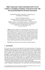
DC Reactor Effect on Bridge Type Superconducting Fault Current Limiter During Load Increasing Tsutomu Hoshino, Khosru·Mohammad Salim, Massanori Nishikawa, Itsuya Muta and Taketsune Nakamura Abstract-In high power application, the fault current limiter has been discussed for many years because of some limitations of conventional circuit breaker. Many types of fault current limiter have already been introduced in papers. In this work, a simple bridge type fault current limiter has been designed and constructed. The performances of the limiter have been tested successfully. In bridge type current limiter, DC reactor appears in the line when connected load is increasing. This causes voltage drop across the load terminal during load changing. The DC reactor effect of the current limiter has been studied. Some experimental results regarding reactor effect of the limiter have been considered and were compared with the results obtained from computer simulation. Keywords- Superconductor, fault current limiter, bridge type, dc reactor.
I.
INTRODUCTION
F
OR highly reliable power supply, fault current limiter (FCL) is becoming an essential part in the modern power system. The conventional technology used today to clear the fault is based on circuit breaker (CB) with over current relay [1]. The typical operational time delay of practical circuit breaker ranges from few cycles to several seconds. During this time, only the system impedance can limit the fault current. Current limiting device is required to be introduced into the power system for limiting the fault current before opening the circuit breaker. Many circuits and theories of FCL have been proposed and some of them are well known. In this paper, attention is drawn on DC reactor type superconducting fault current limiter. The circuit diagram of this bridge type current limiter is shown in Fig. 1. The operational principle of the circuit is discussed elsewhere [2]. The practical difficulty of this circuit is to implement a DC bias source in the bridge circuit [3]. Actually, the DC bias voltage is used to keep the bridge diode continuously conducting at the normal operation. If the amplitude of DC bias current is equal or higher than the peak value of the line current, then the inductor always feeds DC current. Therefore, at normal operation, no current limiting mode occurs. At the time of fault, the fault current goes to higher value and crosses DC bias level. i,From that moment the diodes block the circular current and the DC reactor becomes in-line, i.e. the limiter works in current limiting mode. Without bias source, the peak Manuscript received September 18, 2000. T. Hoshino (+81-75-753-5293,
[email protected]), K. M. Salim (
[email protected]), M. Nishikawa (
[email protected]), 1. Muta (+81-75-753-5292, muta @kuee.kyoto-u.ac.jp), and T. Nakamura (+81-75-753-5294, tLnaka @kuee.kyoto-u.ac.jp) are with the Graduate School of Engineering, Kyoto University, Yoshida Honmachi, Sakyo, Kyoto 606-8501, Japan.
voltage waveform is clipped by the forward voltage drop of the bridge rectifiers. So, the voltage and current waveforms of the current limiter are expected to be distorted at their peaks in normal operation. In this paper, by eliminating the DC bias source, the device is simplified. Now, it is required to observe the device performance at normal operation, especially in case of load changing. As the DC bias source is not used, the increase of load current tries to increase the inductor current. A small change of inductor current produces voltage across inductor that causes voltage drop across the load terminal. The observed load changing effect is a disadvantage of the system at normal operation. To observe this situation, a simple bridge type circuit is constructed and tested. Tests were carried out mainly to monitor the load changing effects. The normal operation of the limiter and the instance of the fault were also observed.
II.
CIRCUIT CONSTRUCTION
The experimental circuit of the superconducting fault current limiter (SFCL) is shown in Fig. 2. In this case, a hybrid bridge circuit is used instead of a simple diode bridge. The hybrid bridge consists of two thyristors Tl and T2 and two diodes Dl and D2. L is the inductance of superconductor coil. The inductance value is 1.2 H. The positive half cycle of current flows through Tl and Dl and the negative half cycle through T2 and D2. The advantage of using the hybrid bridge over the normal diode bridge is that it can also work as fast solid state circuit breaker. In case of high fault current, by removing the gate trigger pulses, the thyristors can shutdown the supply. "Load I" and "Load 2" are connected in parallel. To observe the load changing effect, switch SI is used to connect or disconnect the "Load 2". The solid state switch
Fig. 1. Main circuit of FCL with diode bridge and DC biased superconducting coil.
1051-8223/0 I $1 0.00 © 200 I IEEE
1945 200
25 (e)
J \
\
100
'H (a)
H
In'
Ii
Hybrid Bridge
\\.lj (d/ l~
AC
-100
V
V
U
,........,
,.-,
I'~
'--
I---'
i--J
i--J
(b)
-200
Fig. 2. Constructed circuit diagram of the SFCL.
150
25 250
200 Time (ms)
TABLE I SPECIFICATION OF THE SUPERCONDUCTOR COIL.
Wire Cu ratio Coil hight Inner diameter Outer diameter Rated Magnetic Field Stored Energy Inductance Maximum Voltage Rated Current
NiTiJ(Cu +CuNi) 1/3.3 219 mm 4>96 mm 4>168.5 mm 4.81 T 23.5 kJ 1.175 H 60 V 200 A
S2 is connected across the load terminal to make artificial fault. The specifications of superconductor coil used in this experiment is described in Table 1. In this experiment, the inductance value was chosen 1.2 H. The higher value of inductance produces almost a DC current through the inductor coil. It keeps the diodes continuously conducting. Again, the higher inductance effectively reduces the fault current. On the other hand, the load increasing effect is expected to be worse at higher value of the inductance. The experiment was carried out at liquid helium temperature where the coil was absolutely in superconducting state. In order to avoid the quench of the superconductor coil at fault condition, the change of maximum flux density was restricted to 1 T Is. Using this limitation, the maximum operating voltage and rated current of the coil was calculated as 60 V and 200 A respectively.
III.
Fig. 3. Load increasing effect. (a), (b) and (c) represent the load voltage, load current and inductor current respectively and (d) represents the instance of load change.
to double by switching the "Load 2". From the waveform, before the instance of load change, both the voltage and the current have small "flat" shape at their peak. This is because of the forward voltage drop of the rectifiers in the bridge. After load is increased, the width of the "flat" becomes larger. Due to the increase of load, both the load and inductor currents try to increase. The inductor current can not change abruptly. So, it clips the line current waveform at the point of inductor current level and the bigger "flat" shape appears. It takes some time to reach the inductor current to steady state condition. At steady state, the original shape of the voltage and the current waveforms appear again. Fig. 4 shows the long term effect of the voltage and the current waveforms due to load increase. Fig. 4 (a) represents the voltage and Fig. 4 (b) represents the load current and the inductor current. It takes longer time to
100
EXPERIMENTAL RESULTS
More than 30 tests of load changing effect have been performed and some of the results are presented here. The input voltage ofthe SFCL is set to 60 V. Both "Load I" and "Load 2" are variable resistive type equivalent load. They are set in such a way that it does not cross the maximum current rating of the coil. In the test circuit, "Load I" is continuously connected and "Load 2" is used to perform the load changing test. Using microcontroller, the artificial fault is made at different phase angles. Programmable fault duration time is implemented in software so that different test can be performed at different fault time instants. For testing purpose, the fault interval is arranged from 1 cycle to 30 cycles. Fig. 3 represents the load increasing effect on voltage and current waveforms. To make this test, the load is increased
-100
o
400
200
600
Time (ms) (a) load voltage
25
5
!
o
u
-25
o
200
400
Time (ms) (b) load current and inductor current Fig. 4. Long term effect of load increasing.
600
1946
reach steady state condition of the waveforms because of the higher value of the inductor. As the voltage across the inductor depends on the changing rate of the inductor current, the inductor voltage suddenly increases at the instance of load increasing. This causes the voltage drop across the load. Fig. 4 (a) shows that the load voltage is suddenly reduced at the time of load increased and it recovers exponentially. Load current and inductor current increase at the same rate which is clearly shown in Fig. 4 (b). Fig. 5 depicts the waveforms in load decreasing mode. By disconnecting the switch S2 the papallel "Load 2" is disconnected from "Load 1". After the instance of disconnection, the load voltage increases slightly and suddenly decreases load current as shown in Fig. 5 (a) and (b) respectively. When the load decreases, the inductor current remains at a higher value compared with peak-load current. It means that AC peak value of the current waveform does not cross the inductor current, thus, no current limiting mode occurs. That is why, both the voltage and current waveforms are sinusoidal. Again, when the load is decreased the output voltage increases slightly due to the source impudence effect. Electromagnetic transient simulation of the SFCL is performed to compare the experimental results. Fig. 6 plots the simulation and experimental results of load voltage drop characteristics of bridge type SFCL during load increasing. It is assumed that the source impudence is negligible. The voltage drop is measured at a certain time delay after the moment of load change. In this test, load change is made at zero crossing time and voltage drop is measured at the second peak of the voltage wave after the load change. The simulation is done at different inductance values. The plots show that at a lower value of the inductor, the DC reactor effect is much less on the voltage 100
~ ..,
~
.:a
0
>-
60
~
Q,
40
8
Cl
" ~ >
'0
20
60 100 Load Increased (%)
0
200
400
compared to a higher value of the inductor. The experimental result agreed well with the simulation result at 1.2 H. Slight deviation occurred because the source impudence is neglected in simulation but exists in the actual system. To see the current limiting performance of the SFCL, an artificial fault is made by short-circuiting the load. This is made by turning on the solid state switch Sl of Fig. 2. Fig. 7 shows the output results when fault is made. The graph (a), (b), and (c) represents the voltage, load current and inductor current respectively. (d) indicates the point where the fault is made. Solid state switch Sl consists of thyristors connected in anti-parallel. When it is triggered to make a fault, the thyristors turn on but turn off at zero crossing point. It does not turn on until threshold current is achieved. This is true when the gate signal is continuously on. For this reason some pulse like voltage appear near the zero crossing region at the time of the fault. This is clearly shown in the voltage waveform in Fig. 7 (a). This situation does not appear in the real fault. The result shows that the inductor current (c) increases at certain rate after fault has been made. The peak of the fault current coincides with the inductor current and both have the same rising rate. Longer fault-time effect is shown in Fig. 8. In this case fault duration time is selected to 20 cycles. At this time
600
Time (ms) (a) load voltage
50 _,
100
$ 0
-50 0
200
400
Time (ms) (b) load current and inductor current Fig. 5. Long term effect of load decreasing.
600
-200
-1
I,., (a)
IU
IU
u
u...J
-100
u
,,
1M
Ii'"'
\
L Inductor current
~
140
Fig. 6. Simulation and experimental plots of load voltage drop at different inductance values. The load change is made at zero crossing time and voltage drop is measured at second voltage peak from the instance of load change.
200
-100
E ..,
L= IOmH
0 20
20
(c)
r - .......
(b)
960
U
(d) '--
1000
'--
t-
1040
20
Time (ms)
Fig. 7. Waveforms at the instance offault. (a) load voltage, (b) load current, (c) inductor current and (d) fault point.
1947
I
20
L=50mH
til
.l'l
]
!
-100 800
1200
1000
10
u
1400
]
Tim,' (ms)
Simulation
•
(a) voltage 40
Inductor current
----
••
L
= 1.2 H
Ex e ·men!
10 20 Duration of Fault (cycle)
• 30
20
3:
Fig. 10. Ratio of maximum fault current to initial current at different fault duration time. Higher inductance value shows lower ratio at certain fault time.
o
] -20 -40 800
1000
1400
1200 Time (ms)
(b) fault current and inductor current Fig. 8. Waveforms of long-period fault. Fault duration time is 20 cycles.
the peak fault current reached only twice the normal peak current. This is because the higher value of inductance limits the fault current more effectively. After fault is cleared, the inductor current remains at higher value and slowly decreases to the steady state value. As long as the inductor current is higher than the load current, the shape of the load current becomes undistorted which is clearly shown in Fig. 8 (b). The advantage of using hybrid bridge circuit is that it can be configured as a circuit breaker. Unlike common circuit breakers, this is more faster and can be operated at zerocrossing point. Fig. 9 shows the test result of shutdown effect of the current limiter. In this case, inductor current is sensed for fault detection and shutdown occurs when preset value is achieved. During this test, the preset value for shutdown is set at 1.2 times of the normal current level. The result shows that the limited fault current reached to 200
CONCLUSION
ACKNOWLEDGMENT
The author would like to thank Keisuke Hasegawa and Hiroyuki Yumiya for their cooperation.
(a)
$
1-V
oc
g
u [+--(b)
'-
'-
(d)
-200
IV.
A hybrid bridge type SFCL without DC bias source have been constructed and tested. The test results of the current limiter are presented and discussed. Higher inductance value of superconductor coil is chosen to minimize the fault current. It is observed that a deep voltage drop is occurred on the load terminal during the load increasing time but does not appear during load decreasing. At a lower inductance value, the voltage drop is reduced but it increases the fault current. Load increasing effect is not expected in normal operation. This effect can be eliminated using DC bias current but it is practically difficult to implement a big current source in the bridge circuit.
25
(1)
\00
-\00
the value after 4 cycles of the fault instance. This value is selected just to test the current limiter in protection mode. To detect the actual fault condition, the slope of the rising inductor current also should be measured otherwise the load increasing effect can make a false trigger to shutdown. Fig. 10 shows the plots of simulation and experimental results of maximum fault current at different fault duration time. The simulation is carried out at different inductance values. From the result, the maximum fault current is linearly proportional to the fault duration time. At a certain fault time, the maximum fault current is much higher at the lower inductor value. The experimental data agree well with the data of the simulation at inductance value 1.2 H.
1000
1050
'---
1100
25
Time (ms)
Fig. 9. Shutdown effect after the fault. (a), (b) and (c) are voltage, current and inductor current respectively and (d) is the instant of fault. Trigger signal is shutdown after 4 cycles of the fault point.
REFERENCES [1] T. Ueda, M. Morita et aI., "Solid-sate Current Limiter for Power Distribution System", IEEE Trans. on Power Delivery, vol. 8, no. 4, pp. 1796-1801, Oct. 1993. [2] H. J. Boening and D. A. Paice, "Fault Current Limiter using Superconducting Coil", IEEE Trans. on Magn., vol. MAG-19, no. 3, pp. 1051-1053, May 1983. [3] T. Ishigohka, A. Ninomiya, et aI., "Fabrication and Test of Cryogenic Fault Current Limiter Combining Semiconductors and DC Reactor", Proc. of IPEC-Tokyo 2000, vol. 3, pp. 1525-1528, April 2000.