Received: 4 November 2016
Revised: 31 March 2017
Accepted: 23 April 2017
DOI: 10.1002/dac.3342
RESEARCH ARTICLE
Towards the implementation of Multi‐band Multi‐standard Software‐Defined Radio using Dynamic Partial Reconfiguration Ahmad Sadek1
| Hassan Mostafa1,2,3 | Amin Nassar1 | Yehea Ismail2,3
1
Department of Electronics and Communications Engineering, Cairo University, Giza, Egypt 2
Center of Nano‐electronics and Devices, AUC, New Cairo, Egypt
3 Zewail City of Science and Technology, Giza, Egypt
Correspondence Ahmad Sadek, Department of Electronics and Communications Engineering, Cairo University, Giza, Egypt. Email:
[email protected]
Summary The vast evolution of fixed and mobile standards urges upgrading the hardware to be compatible with them. An efficient approach to reduce the required cost and effort is hardware reusability, which in turn can be achieved by a dynamically reconfigurable field programmable gate array (FPGA). This flexible hardware time multiplexing allows more logic to fit within the same area, which means fitting bigger designs into smaller less expensive devices, with more optimization of power consumption. This work shows the advantages of using the dynamic partial reconfiguration (DPR) technique, on a fine‐grained block level, in implementing a baseband physical layer processing module for software‐defined radio (SDR) chain that supports 3G, long‐term evolution (LTE), and WIFI standards. The benefits increase when the reconfiguration is not only dynamic but also takes place in run‐time without the need to switch off the system. A comparison is held on Xilinx Virtex 5 design kit XUPV5‐LX110T between the implementation of the baseband processing module with and without using the DPR technique in the 3G, long‐term evolution, and WIFI standards. The comparison addresses the area, power, memory, and time overhead. Experimental results reveal that the DPR technique improves the area and the power consumption with an acceptable increase in memory and latency. Xilinx ISE 14.7 is used for modules implementation, Xilinx PlanAhead is used in floorplanning for the different designs and applying the DPR technique, and Xilinx Power Analyzer is used to measure the power consumption. K EY WO R D S 3G, dynamic partial reconfiguration, FPGA, LTE, software‐defined radio, WIFI
1 | INTRODUCTION Wireless communication standards are continuously changing and upgrading to support new features and enable new technologies. Therefore, both of the base station (BS) and the user terminal need to adopt dynamic communication chains capable of supporting multiple standards which are denoted by software‐defined radio (SDR).1 The SDR implementation enables compact system design to reduce the silicon area, the power consumption, and lengthen the battery life. Moreover, SDR implementation makes it easy Int J Commun Syst. 2017;e3342. https://doi.org/10.1002/dac.3342
to accommodate new standards with limited hardware modifications which reduce the production time and cost. The field programmable gate array (FPGA) is a programmable integrated circuit (IC) configured to execute a certain application. The FPGA is considered the best solution to be used in the digital signal processing (DSP) because of its flexibility and efficiency in hardware implementation, where a designer can implement exact 8‐bit data multiplier instead of using 32 bits in the case of digital signal processor. The FPGA reconfigurability allows it to be used in the hardware implementation of SDR.
wileyonlinelibrary.com/journal/dac
Copyright © 2017 John Wiley & Sons, Ltd.
1 of 12
2 of 12
There have been several efforts done in the implementation of SDR using DPR technique. In Delahaye et al,2 the configuration is done using Xilinx column‐based configuration memory, which depends on an old configuration memory array type that needs to configure a complete column instead of certain part. The work done in Delorme et al3 shows FPGA reconfiguration for the encoding block where a study is shown in Sadek et al4 for different MicroBlaze processing frequencies among different communication standards. In Sutton,5 a framework for physical layer and upper layers stack is presented and lists a comparison among IRIS, GNURadio, and OSSIE. In Shreejith et al,6 a prototype is developed on Xilinx Zynq that combines the parametric reconfiguration and the hardware dynamic reconfigurability for fast baseband adaptation. The aim of this work is to show the benefits of using the DPR capability of the FPGA in the implementation of baseband processing module for a multi‐band / multi‐standard SDR mobile system and compare it to the conventional full implementation, where all communication chains processing modules are existing at the same time. A preliminary physical layer processing module for SDR chain is implemented to accommodate 3G, long‐term evolution (LTE), and WIFI, where a run‐time switching occurs among them. The proposed implementation shows a significant decrease in power consumption when compared to the general communication system module (GCSM) that consists of the 3 standards exist separately. The novelty of the proposed design illustrated by breaking down the physical layer of the communication system into fine‐grained blocks where the reconfiguration takes place. Given that some of the blocks are used in some communication standards and not used in others. The presented work studies the power, area, memory, and time overhead in the physical layer of SDR for 2 different designs. The first is based on the DPR technique, and the second uses the conventional communication system. From the area and the power perspectives, using DPR decreases, the used area on the silicon pushing most of the unused blocks to the memory and so the power consumption decreases. Only the communication system, which is in use, will be loaded on the chip. On the other hand, an extra reconfigurable time overhead is needed for loading certain module. And external memory is used to store the communication blocks. The rest of the paper is organized as follows. Sections 2 and 3 give an overview on the cognitive reconfigurable computing and the SDR, respectively. Section 4 shows the similarities of the used communication standards. Section 5 explains the design implementations while the experimental results are presented in Section 6. Section 7 shows the state‐of‐art and future work. Conclusions are drawn in Section 8.
SADEK
ET AL.
2 | COGNITIVE RECONFIGURABLE COMPUTING Reconfigurable computing (RC) term first appears in 1960s when G. Estrin proposed the idea of “fixed plus variable structure”.7,8 His idea considers a fixed hardware processor controls a variable “reconfigurable” hardware arrays. The reconfigurable hardware is configured to deal with a specific task for a certain time, after this time, it will be released to be reconfigured again for another task. This resulted in hybrid hardware‐software computer structure, which combines the software flexibility and hardware efficiency. The FPGA benefits in hardware efficiency and programming flexibility, which allows it to be used in the reconfigurable computing for the SDR. On using DPR, any part of the FPGA can be handled alone during run‐time in a different context while the other FPGA parts are in full functioning. This reconfiguration occurs real time without switching off the FPGA. The advantages of the DPR are its flexibility of redefining the system modules during run‐time functioning, saving power by replacing unused modules, and reducing the cost that is needed to accommodate new designs.9 DPR design factors depend on the FPGA technology and the available tools. In Sadek et al,4 a summary of the DPR factors is shown, and Koch10 shows advanced techniques. Using the DPR technique serves in a self‐adapting SDR system, where SDR is used in the implementation of cognitive radio (CR) to use the available radio frequency spectrum without interfering with the existing users. Using the DPR technique leads to a multi‐band / multi‐standard system, where it can adapt itself by redefining the hardware blocks of the communication chain to accommodate different standards.
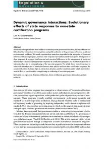
3 | S O F T WA R E ‐ DEFINED RADIO Recently, increasing the connectivity and data sharing among people is the main driving force for the wireless technology progress. This progress includes creating distinct standards such as 2G, 3G, LTE, WIFI, and Bluetooth. Unfortunately, the existence of different standards on the same chip results in reducing the battery life because of the power consumption increases. Also, inefficient utilization of the radio frequency spectrum occurs because the load on the different standards are not equal is some geographical areas taking time into consideration. Different studies are conducted targeting the spectrum utilization,11 management,12 and sensing algorithms.13 In the last 2 decades, there has been extensive work to unify the physical layer and how to reshape it for certain operation where SDR role became important. Figure 1 simplifies the general block diagram of the wireless communication system. The smart antenna, Radio Frequency (RF) front‐end, digital‐to‐analog converter
SADEK
ET AL.
3 of 12
4 | COMMUNICATION STANDARDS SIMILARITIES
FIGURE 1 Ideal communication system. ADC, analog‐to‐digital converter; DAC, digital‐to‐analog converter
(DAC), analog‐to‐digital converter (ADC), and the DSP module. The main focus of this work is on how the DPR enhances the area and power consumption compared to the full implementation method in the DSP module. The waveform is considered the unit of the SDR chain that represents a set of transformations applied to the information at the source to be sent and at the destination to be recovered. These waveforms are stored in external memory and loaded per demand in the DSP block. The ideal SDR chain is shown in Figure 2, where a controller is used to load waveform from n waveforms that are saved in a memory storage. The hardware switching is triggered during the handover between the 2 different communication systems. However, the handover takes hundreds of milliseconds14 while the hardware reconfiguration takes much shorter time (ie, in the microseconds range). On the other hand, many studies have been done on offloading the data traffic between cellular systems, eg, 3G, and fixed wireless systems, eg, WIFI.15
FIGURE 2
Ideal software‐defined radio (SDR) chain
The 2G, 3G, LTE, and WIFI are widely used wireless communication standards. Implementing all these standards on the same integrated circuit results in larger silicon area and higher power consumption for each channel. However, this area and power consumption can be improved if these standards are implemented by using DPR technique. The simple communication channel is formed of channel coding that is used to overcome channel circumstances to retrieve the sent data with accepted accuracy. The second main block is the modulation where a carrier signal adapted in a special way to carry the data signal over the medium to reach its destination. The different communication standards use these main blocks with other blocks depend on specifications of the standard like reaching a high capacity of users with high data rate transfer overcoming the channel circumstances. Simplified communication standards are presented in Figure 3 for the main blocks in the 2G, 3G, 4G, and WIFI standards, where the presented blocks had different specs according to the mode of operation and channel used for each standard. Sections 5 and 6 demonstrate the switching among chosen blocks of 3G, LTE, and WIFI in a reconfigurable system using the Xilinx Virtex 5 design kit XUPV5‐LX110T. The 2G is the wireless mobile second generation standard; it is originally based on the global system for mobile communication (GSM). In the 2G, the physical layer mainly composed of channel coding using convolutional encoder then modulated with Gaussian minimum‐shift keying (GMSK).16 The 3G is the wireless mobile third generation standard; it uses wideband code division multiple access (WCDMA) radio access technology to offer greater spectral efficiency and bandwidth than predecessor 2G. In 3G, the data is encoded using convolutional encoders or Turbo encoders, then it is spread on the channel bandwidth affording better
FIGURE 3 2G, 3G, long‐term evolution (LTE), and WIFI chain summary. DFT, discrete Fourier transform; GMSK, Gaussian minimum‐shift keying; IFFT, inverse fast Fourier transform; LDPC, low‐density parity check code; QAM, quadrature amplitude modulation
4 of 12
channel resistance to noise and interference and then passes through a phase and amplitude modulation technique such as binary phase shift keying (BPSK) and quadrature amplitude modulation (QAM).17 LTE or 4G is the fourth generation in wireless mobile standards. In the LTE uplink transmitter, single carrier frequency division multiple accesses (SC‐FDMA) is used for its lower peak‐to‐average power ratio (PAPR), which in consequence benefits in mobile terminal transmit power efficiency and the power amplifier cost reduction. SC‐FDMA is like the orthogonal frequency division multiple accesses (OFDMA) with discrete Fourier transform (DFT) step is added before layer mapping. The M‐point DFT is selected such that M to be less than N of the N‐point inverse fast Fourier transform (IFFT). The LTE supports different N‐point IFFT sizes for different frequencies18 and different conventional modulation techniques. The LTE uses convolutional encoders and turbo encoders for channel coding.19 WIFI is a fixed wireless communication standard. It allows the electronic devices to exchange data or connect wirelessly to the internet. The WIFI physical layer uses orthogonal frequency division multiplexing (OFDM) as a modulation format. OFDM is a modulation scheme where orthogonal multicarriers closely spaced are used to carry data. Each carrier is modulated using conventional modulation techniques such as BPSK, QAM, and 16‐QAM. The IFFT in the transmitter side is adopted for the carrier orthogonality purpose. Channel coding in WIFI is done using convolutional encoders or low‐density parity check code (LDPC).20 In 2G and 3G, the main blocks are channel coding and modulation. In the LTE, uplink transmitter chain uses the SC‐FDMA channel, which has 2 different main components DFT and IFFT. WIFI depends on the OFDM channel that has an IFFT block. In WIFI and LTE, a mapper is used for mapping frequency points onto the data subcarriers for the
SADEK
ET AL.
OFDM symbol that is assigned to a user. Also, a cyclic prefix (guard insertion) is added to eliminate the inter symbol interference (ISI) between symbols. The puncturing and interleaving stage in different communication standards can be considered as a part of the channel coding.
5 | D E S IG N I MP L E ME N TAT I O N The design implementation is targeting the DSP block of the physical layer that is shown in Figure 1, where Virtex 5 kit XUPV5‐LX110T is used in the implementation of the chosen communication blocks shown in Figure 4. The proposed design shows a preliminary SDR processing system, where a switching is done among 3G, LTE, and WIFI. Figure 4 shows the selected blocks from Figure 3 for 3 standards, which includes the channel coding, modulation, DFT, and IFFT processing stages. These blocks are chosen to be implemented on the FPGA as a start point because these IP cores can be optimized in a library and different communication systems use them. Each standard uses different forms of channel coding, modulation, DFT, and IFFT. The selected channel coding for the different systems is the convolutional encoder. For the 3G standard, 2 different implementations selected, the first with (rate 1/2, constraint length 9) and the second with (rate 1/3, constraint length 9), the LTE convolutional encoder to be implemented with (rate 1/3, constraint length 7), and the WIFI convolutional encoder with (rate 1/2, constraint length 7). The different standards support either BPSK, Quadrature Phase Shift Keying (QPSK), or 16‐QAM as a conventional digital modulation. In the 3G, where it uses the wideband code division multiple access to spread data over the channel and there is no DFT and IFFT blocks, where the later blocks will be replaced by a filler block. In the LTE user equipment (UE) transmitter side M‐Point DFT and N‐Point
FIGURE 4 Selected blocks for 3G, long‐term evolution (LTE), and WIFI. BPSK, binary phase shift keying; DFT, discrete Fourier transform; IFFT, inverse fast Fourier transform; QAM, quadrature amplitude modulation
SADEK
ET AL.
IFFT are used as discussed in Section 4, the selected values for M and N are 64 and 256 respectively. In the WIFI chain, a 64‐point IFFT is used while DFT block is replaced with a filler block. The filler is an empty block added to the chain when no specific block is added. It transfers the inputs to the outputs in the proper time. In the first design shown in Figure 5, a reconfigurable SDR processing chain uses the DPR technique and is denoted as single‐loaded module (SLM). It is composed of 4 successive blocks corresponding to that shown in Figure 4. The chain is composed initially of empty blocks which are ready to host channel coding, modulation, DFT, and IFFT blocks. Each empty block will be filled with the corresponding processing stage for proper operation of the selected standard. Figure 6 shows the schematic of the design, where the selected blocks are adapted to fit within the corresponding host. For example, the designed encoders for the different communication systems had to fit within the host encoder place. The bitstream is fed to the processing module through the in pin shown in Figure 6. The different encoders have developed with a unified interface of 1‐bit input and 2‐bit output. The modulation techniques used by the 3 systems has the same interface of 2‐bit input and 16‐bit output that will be fed to the DFT and then to the IFFT stages, where the DFT and IFFT have 16‐bit inputs and outputs.
5 of 12
The second design shown in Figure 7 is the GCSM. It represents the normal system, where the 3 simplified communication standards exist at the same time and a multiplexer is used to select among them. For minimum GCSM design, a single mode of operation is selected to simulate each standard. Where for implementing the different modes of operation, each standard shall have internal multiplexers to switch among its different blocks in each processing stage and the parametric reconfiguration can be used. For example, the 3G supports different modulation schemes; all had to be exist with a multiplexer to switch among them with more design time and effort for optimizing.
6 | SYSTEM RESULT S The current section presents the results of the SLM and GCSM designs, in area, memory, estimated power consumption, reconfiguration time overhead, and floor‐planned area. The SLM design covers up to 12 design runs for the implementation shown in Figures 4 and 5 for the different combinations per communication standard. Table 1 lists the 12 design runs, where DR_1, DR_2, and DR_3 are 3 design
FIGURE 5 Reconfigurable software‐defined radio (SDR) chain (single‐loaded module (SLM) design). BPSK, binary phase shift keying; DFT, discrete Fourier transform; IFFT, inverse fast Fourier transform; QAM, quadrature amplitude modulation
FIGURE 6
Schematic of software‐defined radio (SDR) processing chain, the thin line for 1‐bit connection and the thick line for n‐bit connections, where n is greater than 1. DFT, discrete Fourier transform; IFFT, inverse fast Fourier transform
SADEK
6 of 12
ET AL.
FIGURE 7 General communication system module (GCSM) design. BPSK, binary phase shift keying; DFT, discrete Fourier transform; IFFT, inverse fast Fourier transform; LTE, long‐term evolution; QAM, quadrature amplitude modulation
TABLE 1 SLM design runs list Design Run
System
Encoder
Modulation
DFT
IFFT
DR_1
3G
3G_half
BPSK
Filler
Filler
Design run
3G
3G_half
QPSK
Filler
Filler
Design run
3G
3G_half
16‐QAM
Filler
Filler
Design run
3G
3G_third
BPSK
Filler
Filler
Design run
3G
3G_third
QPSK
Filler
Filler
Design run
3G
3G_third
16‐QAM
Filler
Filler
Design run
WIFI
WIFI_half
BPSK
Filler
64‐IFFT
DR_2
WIFI
WIFI_half
QPSK
Filler
64‐IFFT
Design run
WIFI
WIFI_half
16‐QAM
Filler
64‐IFFT
Design run
LTE
LTE_third
BPSK
64‐DFT
256‐IFFT
Design run
LTE
LTE_third
QPSK
64‐DFT
256‐IFFT
DR_3
LTE
LTE_third
16‐QAM
64‐DFT
256‐IFFT
Abbreviations: SLM, single‐loaded module; BPSK, binary phase shift keying; DFT, discrete Fourier transform; IFFT, inverse fast Fourier transform; LTE, long‐term evolution; QAM, quadrature amplitude modulation.
runs that are chosen as snapshots to cover a mode of operation for each communication standard. The first design run, DR_1, is for the 3G communication standard with a convolutional encoder of (rate 1/2, constraint length 9) and BPSK modulation. The second design run, DR_2, is for the WIFI with a convolutional encoder of (rate 1/2, constraint length 7), QPSK modulation, and 64‐point IFFT. The third design run, DR_3, is for the LTE with a convolutional encoder of (rate 1/3, constraint length 7), 16‐QAM modulation, 64‐point DFT, and 256‐point IFFT. DR_1 shows the state of the SLM design when the smallest size blocks are loaded for a minimal operation. While the DR_3 represents the SLM design when the largest blocks are loaded at a certain time of the SDR operation. DR_2 is considered a medium case between DR_1 and DR_3.
In the GCSM, a static implementation for the different communication chains is done equivalent to the design runs DR_1, DR_2, and DR_3 for the simplicity of the comparison. While in the real world, each communication standard should be implemented with all its blocks.
6.1 | Area occupied on the FPGA Table 2 shows the number of Look‐Up Tables (LUTs) used by each block in the SLM implementation, the floor‐planned partition that acts as a placeholder for the different modules and the generated bitstream files size. The channel‐coding module is floor planned in 64 LUTs on the FPGA, where the acquired number of LUTs differs from an implementation to another. The floor‐planned LUTs shall be big enough to
SADEK
ET AL.
7 of 12
TABLE 2 SLM design area summary Block type
Block definition
Channel coding
3G convo 1/2 3G convo 1/3 4G convo 1/3 WIFI convo 1/2
Modulation
BPSK QPSK 16‐QAM
DFT IFFT
Number of LUTs
Floor‐planned LUTs
Size, kb
3 11 9 2
64 64 64 64
12.3 12.3 12.3 12.3
3 4 9
64 64 64
12.3 12.3 12.3
64‐point DFT Filler
4674 0
5520 5520
350 350
64‐point IFFT 256‐point IFFT Filler
1811 1871 0
2808 2808 2808
210 210 210
Abbreviations: SLM, single‐loaded module; BPSK, binary phase shift keying; DFT, discrete Fourier transform; IFFT, inverse fast Fourier transform; LTE, long‐term evolution; QAM, quadrature amplitude modulation.
carry the largest module implementation, which is the 3G convolutional encoder of (rate 1/3, constraint length 9). Note that the PlanAhead tool has some routing restrictions that needs to enlarge the area of the planned block. The generated files for the channel coding and modulation blocks are of the same sizes 12.3 KB because the generated files depend on the number of the floor‐ planned LUTs not the acquired LUTs, ie, the 3 LUTs of the convolutional encoder of (rate 1/2, constraint length 9) and the 11 LUTs of the convolutional encoder of (rate 1/3, constraint length 9) both generate files with the same sizes because they are floor planned in 64 LUTs. The DFT is floor planned in 5520 LUTs that will generate a file size of 350 KB. The IFFT is floor planned in 2808 LUTs that will generate a file size of 210 KB. Although the filler block does not acquire physical LUTs but the generated file size is according to the number of the floor‐planned LUTs. At the same time, the filler block does not consume power as there is no LUTs acquired. The channel coding and modulation consume less number of LUTs because the proposed design is processing a single bit at the input for simplicity, where a 32‐bit channel coding is studied in Sadek et al4 using the DPR technique. Using DPR in the SDR chain decreases the number of physical LUTs used on the FPGA. Table 3 summarizes the
area consumed in the 3 selected design runs in the SLM design versus the fixed GCSM design. In the SLM design, on using DPR, because only the used blocks are loaded, the maximum number of LUTs in the case of LTE design run (DR_3) is 6563 LUTs. And the minimum number of LUTs in the 3G design run (DR_1) is 6 LUTs. In the GCSM design, where all blocks exist on the FPGA at the same time, the number of LUTs consumed is 6620 LUTs after XST tool optimization for the selected communication blocks per each standard. This value of 6620 LUTs increases when all the other communication blocks are implemented for the different standards. This shows that the maximum occupied area in the SLM design is nearly equal to the minimum occupied area in the GCSM after tool optimization.
6.2 | Memory needed The chip XC5VLX110T has in total 69120 6‐LUTs;21 this generates a configuration file of size 3.8 MB. Consequently, the initial configuration files for the SLM and GCSM designs have the same size, because they contain all the LUTs in the FPGA chip. In the GCSM design, the FPGA configuration file will remain unchanged during run‐time, because the different systems have their communication blocks exist on
TABLE 3 Number of LUTs used for SLM design runs and GCSM SLM Design run DR_1 (3G standard)
GCSM No. of LUTs
No. of LUTs
6
DR_2 (WIFI standard)
1817
DR_3 (LTE standard)
6563
The 3G, WIFI, and LTE standards exist at the same time.
Abbreviations: GCSM, general communication system module; LTE, long‐term evolution; SLM, single‐loaded module.
6620
SADEK
8 of 12
the FPGA. Therefore, there are no more files that are generated. In the SLM design, the configuration file is used as an initial configuration and contains the static part of the FPGA and the reconfigurable partitions, where the reconfigurable partitions are filled with initial communication blocks and will be reloaded during run‐time with the proper reconfigurable module. Another small files are generated by the PlanAhead tool that contains the reconfigurable modules of each stage of sizes shown in Table 2. Memory needed for SLM design = initial configured chain size + sum (number of communication blocks × size of reconfigurable module per block) = 3.8 MB + 1.4 MB = 5.2 MB. Table 4 summarizes the memory needed for both designs. It shows the needed memory for the SLM design is 5.2 MB, which is equal to the initial configuration chain size and the size of each image for all the communication blocks that are shown in Table 2. In the GCSM design, the bitstream file size is equal to 3.8 MB, and no extra files are needed.
6.3 | Power estimation On using the DPR technique in the implementation of the physical layer of an SDR chain, decreases the number of the physical LUTs that are occupied on the FPGA when compared to the full system implementation. The SLM design occupies a variable number of LUTs on the FPGA according to the loaded modules because the modules are loaded separately, and one scheme of operation exists for TABLE 4 Memory needed for SLM and GCSM SLM
GCSM
Initial configuration bitstream file size = 3.8 MB Reconfigurable bitstream file sizes = 1.4 MB
Configuration bitstream file size = 3.8 MB
Total size = 5.2 MB
Total size = 3.8 MB
Abbreviations: GCSM, general communication system module; SLM, single‐ loaded module.
ET AL.
one standard at a time. Consequently, the power consumed decreases. In the SLM design, the maximum power consumed in the FPGA logic is 128.8 mW, when the LTE standard (DR_3) is loaded. While the minimum power consumed in the FPGA logic is 0.24 mW, when the 3G standard (DR_1) is loaded. Using the DPR technique decreases the power consumption, where the static power dissipation changes according to the different design deployments between 0.24 and 128.8 mW. In the GCSM design, the minimum power consumption is 171 mW for the equivalent design of the selected SLM design runs (DR_1, DR_2, and DR_3) that are shown in Table 1. Where the 3 chains exist on the chip at the same time, and a multiplexer is used to switch among them. The power consumption in the GCSM design increases when each stage in the 3G, WIFI, and LTE standards is fully implemented to carry the different schemes of operation. Table 5 shows the power consumption in the SLM and the GCSM designs. The power consumed in the logic gates is estimated using Xilinx Power Analyzer (XPA) tool. Figure 8 shows the power profile for the SLM and GCSM designs. It shows that the power consumption in the minimal design of the GCSM exceeds the maximum power consumed in the SLM design when the LTE standard (DR_3) is loaded. And the average power consumption for the SLM design equals to 57.11 mW if the 3 standards are loaded equally in time.
6.4 | Time overhead The initial configuration files in the SLM and GCSM designs have the same size because both contains the same number of LUTs, then both designs have the same initial configuration time. Xilinx Virtex 5 FPGAs have different configuration modes, external and internal.22 A study compares the different configuration modes for Xilinx Virtex FPGAs 5 is presented in Hassan et al,23 another comparison targeting internal partial reconfiguration controllers for Xilinx Zynq FPGA is presented in Kamaleldin et al.24 JTAG is an external configuration mode with maximum throughput 8.25 MBps22 is used for the simplicity of the design.
TABLE 5 Power consumption for SLM design runs and GCSM SLM Design run
GCSM Power consumed in logic, mW
DR_1 (3G standard)
0.24
DR_2 (WIFI standard)
42.49
DR_3 (LTE standard)
128.8
Power consumed in logic, mW
The 3G, WIFI, and LTE standards exist at the same time.
Abbreviations: GCSM, general communication system module; LTE, long‐term evolution; SLM, single‐loaded module.
171.47
SADEK
ET AL.
9 of 12
TABLE 6 Configuration and reconfiguration time in SLM and GCSM designs SLM
GCSM
Initial configuration time using JTAG = 460 ms
Initial configuration time using JTAG = 460 ms
MTRT using JTAG = 70.86 ms
MTRT using JTAG = 0
Initial configuration time using ICAP = 95 ms
Initial configuration time using ICAP = 95 ms
MTRT using ICAP = 1.46 ms
MTRT using ICAP = 0
Abbreviations: GCSM, general communication system module; MTRT, maximum theoretical reconfiguration time; SLM, single‐loaded module.
FIGURE 8 Power profile for the single‐loaded module (SLM) and general communication system module (GCSM) designs. In the GCSM design, the 3 communication standards exist at the same time as shown in Figure 9, where in the SLM design, 1 communication standard is loaded at a time as shown in Figure 10. The average power consumption in the SLM design is one‐third the power consumption in the GCSM design. LTE, long‐term evolution
The initial configuration time using JTAG = the initial configuration file size/maximum throughput of the JTAG = 3.8 MB/8.25 MBps = 460 millseconds. The initial configuration time is reduced on using high speed internal configuration mode such as ICAP to 1.46 milliseconds, where the ICAP maximum throughput equals 400 MBps.22 In the GCSM, there is no reconfiguration time overhead added after the initial configuration, because all the communication blocks of the different standards are existing on the chip. In the SLM design, the reconfiguration time overhead is the time needed to reconfigure a communication block in the SDR chain. The maximum theoretical reconfiguration time (MTRT) is the time needed to reconfigure all the SLM design blocks. MTRT in SLM = summation of the reconfigurable block sizes/configuration mode throughput using JTAG = (12.3 + 12.3 + 350 + 210) KB/ 8.25 MBps = 70.86 milliseconds. On using the ICAP, as a configuration mode for the FPGA with maximum throughput 400 MBps, the MTRT value decreases to 1.46 milliseconds. Table 6 summarizes the configuration and reconfiguration time for the SLM and GSCM designs using JTAG and ICAP configuration modes.
6.5 | Floorplanning Figure 9 shows the GCSM design floorplanning on Virtex 5 kit XUPV5‐LX110T for the physical layer of the 3 wireless systems 3G, WIFI, and LTE. The 3 systems are existing on
FIGURE 9
General communication system module floorplanning. The 3 standards exist on the field programmable gate array at the same time. Each standard contains its internal blocks fully implemented with the different combinations. LTE, long‐term evolution
the chip at the same time, although they are not operating at the same time. Their existence will occupy more LUTs that leads to more static power dissipation. In the proposed design for the physical layer; the 3G chain acquires the smallest area because it consists of channel coding block and modulation block. The WIFI chain consists of the channel coding block,
SADEK
10 of 12
modulation block, and IFFT block. The LTE chain consists of the channel‐coding block, modulation block, DFT block, and IFFT block. Figure 10 shows the SLM design floorplanning on Virtex 5 kit XUPV5‐LX110T. It shows improvement in the area that will reflect on decreasing power dissipation as well. Where only the used modules, for either 3G, WIFI, or LTE, will be loaded during run‐time on the chip. Figure 10 shows the floorplanning of the 4 building blocks of the SLM design that is presented in Figures 4, 5, and 6, which are the channel coding block, modulation block, DFT block, and IFFT block. These blocks carry one implementation per time. Figure 10A shows the deployment of the 3G standard, where the channel coding block is loaded with the convolutional encoder of (rate 1/2, constraint length 9) or (rate 1/3, constraint length 9). The modulation block is loaded with either BPSK, QPSK, or 16‐QAM as stated in Table 2. The DFT block and the IFFT block are loaded with filler module that does not consume area and power; therefore, they seem like empty blocks. In Figure 10B, the WIFI standard is deployed on the chip. The channel coding block is loaded with the convolutional encoder of (rate 1/2, constraint length 7), and the modulation block is loaded with either BPSK, QPSK, or 16‐QAM. It clearly appears that the IFFT block is populated with the 64‐point IFFT module. Because the DFT block is not used in the WIFI standard, a filler block is loaded instead. In Figure 10C, the LTE standard is deployed. The channel coding block is loaded with the convolutional encoder of (rate 1/3, constraint length 7), and the modulation block is loaded with either BPSK, QPSK or 16‐QAM. The DFT block
ET AL.
is loaded with the 64‐point DFT, and the IFFT block is loaded with the 256‐point IFFT. This shows that the LTE consumes the largest number of LUTs on the FPGA. Therefore, if the deployment of the LTE is delayed till its time of operation, this will lead to decrease the power consumption.
7 | STATE‐ OF‐T H E‐A RT AN D FUTURE WORK There are several SDR architectures based on GPP, DSP, and FPGA. In Anjum et al25 and Ramacher,26 various architectures of implementing SDR chains are surveyed. Examples of reconfigurable SDR include Montium,27 Butter/ CREMA,28 and HERS.29 These implementations are based on coarse‐grained FPGA modules, which adapt the baseband modules according to the running algorithm. Other commercial SDR platforms are presented in Sklivanitis et al30 describing different software and hardware architectures needed to support SDR. A novel mechanism called RF network‐on‐chip (RFNOC) is developed in Braun et al31 for reconfigurable FPGAs. RFNOC is an open source framework used to offload baseband signal processing blocks on the FPGA. This framework drives reconfigurable FPGAs, where user‐defined blocks are deployed for proper operation. RFNOC is a promising framework for the DPR approach, where more integration is needed between RFNOC and Xilinx tools to develop and define the reconfigurable partitions. Software‐defined radio solutions are pushing their ways towards mobile communications systems, where new standards are being developed to accommodate the
FIGURE 10 Dynamic partial reconfiguration (DPR) design runs floorplanning. Initially, 1 standard is loaded and switching occurs during run‐time of operation. A, DR_1, the channel coding and modulation blocks are loaded with the corresponding blocks during the operation of 3G, where the discrete Fourier transform (DFT) and inverse fast Fourier transform (IFFT) are empty blocks. B, DR_2, the channel coding, modulation, and IFFT blocks are loaded with the corresponding blocks during the operation of WIFI, where the DFT is empty. C, DR_3, all the blocks are loaded during the operation of long‐term evolution (LTE)
SADEK
ET AL.
staggering number of users and their growing needs for higher data rates. Furthermore, UE designs need to maintain several desirable features, eg, small sizes, connectivity, and low‐power consumption for longer battery operation time. The 5G is a new player in the mobile communications market with 2 main enabling technologies: massive MIMO and millimeter‐wave communications. The 5G solutions are expected to hit the market by 2020.32 In 5G, the BS is required to serve many users with various preferences. Under mobility conditions, channel characteristics and traffic conditions are likely to change over time. Hence, the UE design should be flexible and adaptive enough to quickly accept any updates in channel conditions or serving cells. The proposed SDR‐based solution enables UEs to switch among different available BSs in the same geographical area to offload the macro‐BS and redistribute the load to small cell BSs.33 The DPR allows the UE to easily adapt to channel and traffic updates and, moreover, leads to tailored low‐ power circuits. The device easily integrates into different layers of communication systems.
8 | CONCLUSION The DPR technique is a flexible and an efficient way of realizing SDR physical layer in a cognitive radio system. It helps in the utilization of the hardware area on silicon, power savings, and frequency spectrum utilization. Also, it would help in offloading between cellular systems and fixed wireless systems, not only on the network level but also on the hardware level. Using DPR produces reconfigurable devices that can adapt different communication standards with the concept of plug and play. Hereby, the communication systems can be divided into fine‐grained blocks and a library of standard IPs for the different communication blocks. The injection of these blocks on a fine‐grained level reduces the system design complexity and makes it maintainable and real‐time upgradable.
11 of 12
2. Delahaye J, Moy C, Leray P, Palicot J. Managing dynamic partial reconfiguration on heterogeneous SDR platforms. SDR Forum Technical Conference Vol. 5. 2005. 3. Delorme J, Martin J, Nafkha A, et al. A FPGA partial reconfiguration design approach for cognitive radio based on NoC architecture. Circuits and Systems and TAISA Conference, 2008. NEWCAS‐TAISA 2008. 2008 Joint 6th International IEEE Northeast Workshop on. IEEE, 2008. 4. Sadek A, Mostafa H, Nassar A. Dynamic channel coding reconfiguration in software defined radio. In 2015 27th International Conference on Microelectronics (ICM), Casablanca, Morocco, IEEE, 2015; 13–16. 5. Sutton P D, Lotze J, Lahlou H, et al. Iris: an architecture for cognitive radio networking testbeds. IEEE Commun Mag. 2010;48(9):114‐122. 6. Shreejith S, Banarjee B, Vipin K, Fahmy S A. Dynamic cognitive radios on the Xilinx Zynq hybrid FPGA. International Conference on Cognitive Radio Oriented Wireless Networks. Springer International Publishing, 2015. 7. Estrin G. Organization of computer systems: the fixed plus variable structure computer. in Papers presented at the May 3‐5, 1960, western joint IRE‐AIEE‐ACM computer conference 1960; 33–40, ACM. 8. Estrin G. Reconfigurable computer origins: the UCLA fixed‐plus‐ variable (f + v) structure computer. IEEE Ann Hist Comput. 2002;(4):3‐9. 9. Dye D. Partial reconfiguration of Xilinx FPGAs using ISE design suite. WP374 (v1.2), May 30, 2012. 10. Koch D. Partial reconfiguration on FPGAs: architectures, tools and applications. vol. 153. Springer Science & Business Media, 2012. 11. Valenta V, Maršálek R, Baudoin G, Villegas M, Suarez M, Robert F. Survey on spectrum utilization in Europe: measurements, analyses and observations. Cognitive Radio Oriented Wireless Networks & Communications (CROWNCOM), 2010 Proceedings of the Fifth International Conference on. IEEE. 2010. 12. Akyildiz I F, Lee W Y, Vuran M C, Mohanty S. A survey on spectrum management in cognitive radio networks. IEEE Commun Mag. 2008;46(4). 13. Yucek T, Arslan H. A survey of spectrum sensing algorithms for cognitive radio applications. IEEE Commun Surv Tutorials. 2009;11(1):116‐130.
AC KN OWL ED GE M EN TS
14. Janevski T. Traffic analysis and design of wireless IP networks. Artech House. 2003.
We thank our colleagues from the British University in Egypt (BUE): Hamza A. Elhawary, Mostafa El‐Naggar, and Osama Youssef for their support in writing some codes. This work was partially funded by Zewail City of Science and Technology, AUC, Cairo University, NTRA, ITIDA, SRC, ASRT, the STDF, Intel, Mentor Graphics, MCIT, and NSERC.
15. Balasubramanian A, Mahajan R, Venkataramani A. Augmenting mobile 3G using WiFi. Proceedings of the 8th international conference on Mobile systems, applications, and services, ACM. 2010; 209‐222.
R E F E RENC E S 1. Mitola J. The software radio architecture. IEEE Commun Mag. 1995;33(5):26‐38.
16. Digital cellular telecommunications system (phase 2+); physical layer on the radio path; general description. 3GPP TS 45.001 version 12.1.0 Release 12. 17. Universal mobile telecommunications system (UMTS); physical layer —General description. 3GPP TS 25.201 version 12.0.0 Release 12. 18. LTE; evolved universal terrestrial radio access (E‐UTRA); user equipment (UE) radio transmission and reception. 3GPP TS 36.101 version 12.9.0 Release 12.
12 of 12
19. LTE; evolved universal terrestrial radio access (E‐UTRA); LTE physical layer; general description. 3GPP TS 36.201 version 12.0.0 Release 12. 20. Wireless LAN medium access control (MAC) and physical layer (PHY) specifications. IEEE Computer Society LAN MAN Standards Committee and others. 21. Xilinx Inc., Virtex 5 FPGA User Guide UG190. v5.4, March 2012. 22. Xilinx Inc., Virtex 5 FPGA Configuration User Guide UG191. v3.11, October 2012. 23. Hassan A, Ahmed R, Mostafa H, Fahmy HAH, Hussien A. Performance evaluation of dynamic partial reconfiguration techniques for software defined radio implementation on FPGA. 2015 IEEE International Conference on Electronics, Circuits, and Systems (ICECS), Cairo. 2015; 183‐186. 24. Kamaleldin A, Mohamed A, Nagy A, Gamal Y, Shalash A, Mostafa H. Design guidelines for the high‐speed dynamic partial reconfiguration based software defined radio implementations on Xilinx Zynq FPGA. 2017 IEEE International Symposium on Circuits and Systems (ISCAS), Baltimore, Maryland, USA. 2017, in publication. 25. Anjum O, Ahonen T, Garzia F, Nurmi J, Brunelli C, Berg H. State of the art baseband DSP platforms for software defined radio: A survey. EURASIP J Wirel Commun Netw. 2011;(1):5 2011 26. Ramacher U. Software‐defined radio prospects for multistandard mobile phones. Computer. 2007;40(10): 27. Rauwerda GK, Smit GJM, van Bentham CRW, Heysters PM. Reconfigurable turbo/viterbi channel decoder in the coarse‐grained montium architecture. in Proceedings of the International Conference on Engineering of Reconfigurable Systems and Algorithms (ERSA'06), Las Vegas, Nevada, USA, June 2006.
SADEK
ET AL.
28. Brunelli C, Cinelli F, Nurmi J. A VHDL model and implementation of a coarse grain reconfigurable coprocessor for a RISC core. in Proceedings of the 2nd Conference on Ph.D. Research in MicroElectronics and Electronics (PRIME), June 2006; 229–232. 29. Niktash A, Parizi HT, Bagherzadeh N. Application of a heterogeneous reconfigurable architecture to OFDM wireless systems. in Proceedings of the IEEE International Symposium on Circuits and Systems (ISCAS) 2007, New Orleans, pp. 2586–2589, 27–30 May 2007. 30. Sklivanitis G, Gannon A, Batalama SN, Pados DA. Addressing next‐generation wireless challenges with commercial software‐ defined radio platforms. IEEE Commun Mag. 2016;54(1):59‐67. 31. Braun M, Pendlum J, Ettus M. RFNoC: RF network‐on‐chip. Proc GNU Radio Conf. 2016;1(1): http://pubs.gnuradio.org/index.php/ grcon/article/view/3 32. Alliance NGMN. “NGMN 5G white paper v1. 0,” approved and delivered by the NGMN board, 17th Feb 2015. 33. Han T, Han Y, Ge X, et al. Small cell offloading through cooperative communication in software defined heterogeneous networks. IEEE Sensors J. 2016;16(20):7381‐7392.
How to cite this article: Sadek A, Mostafa H, Nassar A, Ismail Y. Towards the implementation of multi‐band multi‐standard software‐defined radio using dynamic partial reconfiguration. Int J Commun Syst. 2017;e3342. https://doi.org/10.1002/dac.3342