Jul 19, 2010 - ... delocalized and localized elec- tron states can be realized and controlled in these ar-. arXiv:1007.3168v1 [cond-mat.mes-hall] 19 Jul 2010 ...
Delocalized-localized transition in a semiconductor two-dimensional honeycomb lattice G. De Simoni,1 A. Singha,1 M. Gibertini,1 B. Karmakar,1 M. Polini,1 V. Piazza,1 L.N. Pfeiffer,2 K.W. West,2 F. Beltram,1 and V. Pellegrini1 1)
NEST, Istituto Nanoscienze-CNR and Scuola Normale Superiore, I-56127 Pisa, Italy 2) Department of Electrical Engineering, Princeton University, NJ USA
arXiv:1007.3168v1 [cond-mat.mes-hall] 19 Jul 2010
(Dated: 20 July 2010)
We report the magneto-transport properties of a two-dimensional electron gas in a modulation-doped AlGaAs/GaAs heterostructure subjected to a lateral potential with honeycomb geometry. Periodic oscillations of the magneto-resistance and a delocalized-localized transition are shown by applying a gate voltage. We argue that electrons in such artificial-graphene lattices offer a promising approach for the simulation of quantum phases dictated by Coulomb interactions. Magneto-transport properties of two-dimensional electron systems confined in semiconductor heterostructures and subjected to quantizing in-plane potentials were extensively investigated1–5 . Recently renewed interest on these systems was triggered by theoretical proposals for the realization of quantum simulators in scalable solidstate systems6–8 . These authors discussed the evaluation of Coulomb interaction strength and hopping properties of electrons confined in square arrays of coupled GaAs quantum dots or at the minima of standing waves created by surface acoustic waves. Such quantum simulators can represent a viable strategy to investigate quantum phases and many-body effects in a controlled way9,10 and may open the way to the emulation of quantum phenomena not easily accessible in nature. To date, however, experimental tests of quantum simulators were carried out only in few systems including in particular cold atoms11,12 and trapped ions13 . Here we report on the fabrication and magnetotransport characterization of a scalable quantum simulator obtained in a modulation-doped high-mobility GaAs semiconductor heterostructure. The structure consists of an array of pillars with honeycomb symmetry that are formed on the surface of the semiconductor by shallow etching. Owing to the dependence of band-bending profiles on GaAs cap-layer thickness14 , these nanofabricated pillars induce a lateral potential modulation (V0 ) of amplitude of few meV’s acting on the electronic system. This lateral potential manifests itself by the appearance of a modulation of the magneto-resistivity that is periodic in the magnetic field. We shall show that a transition from a conducting to an insulating regime can be induced by changing the voltage of a metallic gate deposited on top of the array. Our experimental findings suggest that while electrons occupy delocalized states at low values of the gate voltage (i.e. when carrier density is high and V0 is small), they localize in the confined levels of the potential minima underneath the pillars as we sweep the gate voltage and increase |V0 |. This interpretation is supported by theoretical evaluations of the hopping parameters for these quantum-confined states.
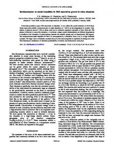
(b)
(a) 60 nm
2r0 = 60 nm
J±1 J0
V0
a = 130 nm
500 nm
(c)
(d)
FIG. 1. (a) Sketch of the lateral potential with relevant geometrical parameters. Jα denotes the hopping parameter and α = {n, m} a set of quantum numbers (see text). (b) Scanning electron microscopy image of the nanopatterned modulationdoped GaAs/AlGaAs sample with honeycomb geometry. The inset shows a picture of the device with four Ohmic contacts. (c) Calculated bound-state energy levels Eα as functions of |V0 |. Different curves correspond to different values of the angular momentum m: m = 0 (blue circles), m = ±1 (red triangles), m = ±2 (green hexagons), and m = ±3 (yellow squares). Curves corresponding to m values which differ only by a sign are degenerate. For a fixed value of V0 curves with same symbol and color coding but higher energy correspond to excited states with different radial quantum numbers. (d) The hopping integrals Jα as functions of |V0 |. Symbol coding is the same as in panel (c). The horizontal dashed line labels the thermal energy at T = 250 mK. Vertical dashed lines mark the threshold values of V0 at which a new bound state appears. The color of the dashed lines is related to the value of m as in panel (c).
The demonstration that delocalized and localized electron states can be realized and controlled in these ar-
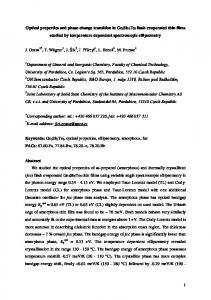
Rxx (k!)
B (T) 0.5 1.0 1.5 (c) 1.0
1.6 (a) 1.2
0.8
0.8
0.6
0.4
0.4 50 (b) 0 -50 1.2 1.4 B (T)
9 6 3
0.2
Index
"Rxx (!)
tificial honeycomb lattices with the same topology of graphene15 opens up exciting opportunities for the study of unusual electronic phases and collective modes induced by the lattice potential at ultra-low temperatures and for the simulation of massless Dirac fermion15 ground states in the presence of external fields. Of particular relevance is the possibility to explore a regime of strong correlations that is not easily achievable in graphene and is characterized by inter-pillar hopping being much smaller than the on-site Coulomb energy. The sample used in this study contains a twodimensional electron gas (2DEG) in a 25 nm wide, one-side modulation-doped Al0.1 Ga0.9 As/GaAs quantum well (QW). The 2DEG is positioned 170 nm underneath the surface (the doping layer is at 110 nm). It has lowtemperature electron density ne = 1.1 × 1011 cm−2 and mobility of 2.7 × 106 cm2 /(Vs). The in-plane potential modulation was achieved by defining an array of Nickel disks (with diameter 2r0 ) arranged in a honeycomblattice geometry (with lattice constant a) by e-beam nanolithography and then by etching away the material outside the disks by inductive coupled reactive ion shallow etching15,16 . Different etching depths d were realized. Results presented here were obtained with d = 60 nm [see Fig. 1(a)]. Larger etching depth lead to electron localization even at zero gate voltage. The resulting lateral nano-patterning after removal of the Nickel, which extends on a 100 µm × 100 µm square region, is shown in Fig. 1(b). Experimental values of the parameters are a ∼ 130 nm and r0 ∼ 30 nm. In order to probe the transport properties of the device, Ni/AuGe/Ni/Au (10/180/10/100 nm) annealed ohmic contacts were evaporated at the corners of the array [see inset of Fig. 1(b)]. Other contacts were realized off the array where the 60 nm-thick GaAs layer was uniformly etched away. Thanks to the low level of damage introduced by this process16 , the 60nm-thick pillars of the honeycomb array act as a weak attractive potential (V0 < 0) for electrons. The absence of any signature of conductive behavior outside the array (data not shown) suggests that when the etching affects the whole sample surface it is sufficient to fully deplete the QW. We therefore estimate V0 ≈ EF ≈ 4 meV where EF is the Fermi energy of the original unperturbed 2DEG. A 120 nmthick Al gate was deposited on top of the device to allow the tuning of the charge density and V0 . Electrical measurements were performed by a lock-in technique in a filtered 3 He magneto-cryostat with 250 mK base temperature. While the overall behavior was the same after different cool-downs with different illumination procedures, the values of the charge density at a given gate voltage were found to change from cool-down to cool-down. Figure 2(a) shows a representative low-temperature longitudinal magneto-resistance characteristic measured at gate voltage Vg = −1.62 V. The observation of distinct quantum Hall signatures with an estimated electron density of 4.5 × 1010 cm−2 demonstrates the existence of delocalized states populated by electrons at this den-
0.0 30 60 90 -1 Frequency (T )
dRxx/dB Power spectrum (a.u.)
2
FIG. 2. (a) Longitudinal resistance Rxx as a function of the magnetic field at a gate voltage Vg = −1.62 V and charge density n = 4.6 × 1010 cm−2 . (b) A magnified portion of data between 1.1 T and 1.5 T. A polynomial fit of the main Rxx curve was subtracted to enhance the visibility of magnetic-fieldperiodic oscillation. A scatter-plot of the resistance minima position is also shown. (c) Device oscillation power spectrum obtained by applying the Fast Fourier Transform algorithm on a set of dRxx /dB taken at several gate voltages (from −1.2 to −1.62 V, corresponding to n = 4.8 and 4.5×1010 cm−2 , respectively). Contributions from all curves have been averaged to reduce the spectral noise.
sity. Weak modulations of the resistivity [highlighted in Fig. 2(b)] in the magnetic-field range between filling factors ν = 2 and ν = 1 are present and appear only below a certain gate voltage. In Fig. 2(c) we report the averaged Fast Fourier Transform (FFT) relative to a set of dRxx /dB traces taken from Vg = −1.2 V to −1.62 V. Two main peaks are observed at 27 T−1 (FWHM 6 T−1 ) and 67 T−1 (FWHM 20 T −1 ) corresponding, respectively, to 2.5 and 6.5 times the geometrical area of the hexagonal unit cell. Following early works based on a semiclassical analysis4,17 , the FFT peaks can be attributed to the quantization of periodic orbits, although a precise identification requires a more extended theoretical investigation. We now address the evolution of the carrier density as a function of Vg in a set of two-wire quantum Hall measurements. The results presented in Fig. 3 display the expected decrease of the charge density above a threshold gate voltage whose value is associated with the depletion of the residual charge trapped in the Si doping layer. We remark that as we lower Vg the resistance becomes so high that it hinders a reliable estimate of the electron density. This is consistent with a transition to a regime of electrons localized in the minima of the honeycomb potential as supported by the finite density of 2.5 − 3 × 1010 cm−2 found in the transition region at Vg ≈ −1.5 V . We remark that the two-wire configuration setup allows us to estimate the charge density even
3
-2
4 .0 V g (V ) 1 0 1 0
6
1 0
5
1 0
4
3 .5 3 .0
R
( Ω)
-1 .5 -1 .0 -0 .5 7
-1 .5
2 .5
C a r r ie r D e n s ity ( 1 0
c m
4 .5
1 0
)
in this transition region. This is otherwise impossible because of the non-linear behavior of the voltage-probe contacts in that regime. In order to investigate in more detail the transition to the localized-insulating regime we present in the inset to Fig. 3 the sample resistance as a function of Vg at zero perpendicular magnetic field. A transition associated to an abrupt increase of the sample resistance leads to a persistent insulating state. While the transition threshold was observed to depend weakly (±200 mV) on the cool-down/illumination procedure, the qualitative behavior remains the same from cool-down to cooldown. The sample can be driven again to the conductive/delocalized regime by means of a thermal cycle (250 mK − 30 K − 250 mK) or by illumination. This latter behavior can be related to the presence of several trapping mechanisms largely due to the device fabrication steps. The insulating behavior highlighted in Fig. 3 can be explained in terms of electron localization in the confined levels of the potential minima as shown in Fig. 1(a). To confirm this picture, which requires negligible inter-site hopping between the confined levels of neighboring minima, we evaluated the hopping integrals between states in two pillars placed at a relative center-to-center distance equal to a. To this end, the external potential created by a single pillar was modeled by a simple rotationallyinvariant piecewise-constant function of the 2D position r: Vext (r) = V0 if r = |r| < r0 and zero otherwise. The resulting eigenfunctions are particularly simple in polar coordinates (r, θ), where they can be written as18
-1 .0 -0 .5 V g (V )
FIG. 3. Carrier density (after a representative cooldown) as a function of gate voltage Vg at T = 250 mK. The inset shows the behavior of the longitudinal resistance measured via a two-terminal setup as a function of Vg at 250 mK and zero magnetic field. The localized regime is achieved below Vg = −1.5 V.
√ Φα (r) = ψn,m (r)χm (θ), χm (θ) = eimθ / 2π, with m a relative integer, being the eigenstates of the angular moˆ z = −i~∂/∂θ along the zˆ direction. mentum operator L The spectrum of bound states with energy Eα < 0 can be found by solving the following transcendental equation: k
0 Jm (kr0 ) K 0 (κr0 ) =κ m . Jm (kr0 ) Km (κr0 )
(1)
Here k = [2mb (|V0 | − |Eα |)/~2 ]1/2 , κ = (2mb |Eα |/~2 )1/2 , mb is the band mass, and Jm (x), Km (x) are standard 0 0 Bessel functions [Jm (x) and Km (x) begin their derivatives with respect to x]. The spectrum Eα obtained by solving Eq. (1) is reported in Fig. 1(c) as a function of V0 for various values of the angular momentum m. The hopping parameter Jα , which provides the rate at which tunneling occurs from a pillar to a neighboring one, can be calculated from the following two-center integral Z Jα = d2 r Φ∗α (r)Vext (r)Φα (r − a) . (2) Here Φα (r) are the eigenstates of a single pillar centered at the origin and a is a nearest-neighbor position vector. Numerical results for Jα are reported in Fig. 1(d). We see that in the relevant range of potential depths, V0 ≈ 5 meV, the hopping integral associated with the two lowest bound state is smaller than the thermal energy (horizontal dashed line). In the presence of a magnetic field B = B zˆ it is easy to show via a gauge transformation that Z ϕ(r) (3) Jα = d2 r e2πi ϕ0 Φ∗α (r)Vext (r)Φα (r − a) , where we have defined ϕ(r) = B·(r×a)/2 and ϕ0 = ~c/e is the flux quantum. The complex phase factor in Eq. (3), which resembles the Peierls phase, and the magnetic-field dependence of the eigenstates Φα (r) lead to a further (exponential) suppression of Jα (data not shown). In conclusion, we have studied electron transport in a high-mobility GaAs quantum well in which electrons are subjected to a lateral artificial potential with honeycomb geometry. The possibility to control the localized/delocalized nature of the electronic states suggests further use of this system for quantum simulations in a regime dominated by electron correlations. Acknowledgements.— We thank A. Pinczuk for useful discussions. 1 C.
Albrecht et al., Phys. Rev. Lett. 86, 147 (2001). Melinte et al., Phys. Rev. Lett. 92, 036802 (2004). 3 R. R. Gerhardts et al., Phys. Rev. Lett. 62, 1173 (1989). 4 D. Weiss et al., Phys. Rev. Lett. 70, 4118 (1993). 5 E. Paris et al., J. Phys.: Condens. Matter 3, 6605 (1991). 6 T. Byrnes et al., Phys. Rev. Lett. 99, 016405 (2007). 7 T. Byrnes et al., Phys. Rev. B 78, 075320 (2008). 8 I. Buluta and F. Nori, Science 326, 108 (2009). 9 R. P. Feynman, Int. J. Theor. Phys. 21, 467 (1982). 10 S. Lloyd, Science 274, 1073 (1996). 11 M. Greiner et al., Nature 415, 39 (2002). 2 S.
4 12 G.
B. Jo et al., Science 325, 1521 (2009). Friedenauer et al., Nature Phys. 4, 757 (2008). 14 L. P. Rokhinson et al., Superlattices and Microstructures, 32, 99 (2002). 15 M. Gibertini et al., Phys. Rev. B 79, 241406(R) (2009). 16 C. P. Garcia et al., Phys. Rev. Lett. 95, 266806 (2005). 13 A.
17 R.
Fleischmann, T. Geisel, and R. Ketzmerick, Phys. Rev. Lett. 68, 1367 (1992). 18 α = {n, m} denotes a set of quantum numbers comprising the radial quantum number n (which sets the zeroes of the radial wavefunction ψn,m (r) and the angular momentum quantum number m.