Access to external memory is handled via a. 25.6GB/s XDR memory controller. The PowerPC core, the eight SPE's, the DRAM controller, and I/O controllers.
Lawrence Berkeley National Laboratory (University of California, University of California) Year
Paper LBNL-
Dense and Sparse Matrix Operations on the Cell Processor Samuel W. Williams
John Shalf
Parry Husbands
Leonid Oliker
Katherine Yelick
This paper is posted at the eScholarship Repository, University of California. http://repositories.cdlib.org/lbnl/LBNL-58253 c Copyright 2005 by the authors.
Dense and Sparse Matrix Operations on the Cell Processor Abstract The slowing pace of commodity microprocessor performance improvements combined with ever-increasing chip power demands has become of utmost concern to computational scientists. Therefore, the high performance computing community is examining alternative architectures that address the limitations of modern superscalar designs. In this work, we examine STI’s forthcoming Cell processor: a novel, low-power architecture that combines a PowerPC core with eight independent SIMD processing units coupled with a software-controlled memory to offer high FLOP/s/Watt. Since neither Cell hardware nor cycleaccurate simulators are currently publicly available, we develop an analytic framework to predict Cell performance on dense and sparse matrix operations, using a variety of algorithmic approaches. Results demonstrate Cell’s potential to deliver more than an order of magnitude better GFLOP/s per watt performance, when compared with the Intel Itanium2 and Cray X1 processors.
DISCLAIMER This document was prepared as an account of work sponsored by the United States Government. While this document is believed to contain correct information, neither the United States Government nor any agency thereof, nor The Regents of the University of California, nor any of their employees, makes any warranty, express or implied, or assumes any legal responsibility for the accuracy, completeness, or usefulness of any information, apparatus, product, or process disclosed, or represents that its use would not infringe privately owned rights. Reference herein to any specific commercial product, process, or service by its trade name, trademark, manufacturer, or otherwise, does not necessarily constitute or imply its endorsement, recommendation, or favoring by the United States Government or any agency thereof, or The Regents of the University of California. The views and opinions of authors expressed herein do not necessarily state or reflect those of the United States Government or any agency thereof or The Regents of the University of California.
Dense and Sparse Matrix Operations on the Cell Processor Samuel Williams, John Shalf, Leonid Oliker, Parry Husbands, Katherine Yelick Lawrence Berkeley National Laboratory 1 Cyclotron Road Berkeley CA, 94720
{SWWilliams, JShalf, LOliker, PJRHusbands, KAYelick}@lbl.gov Abstract The slowing pace of commodity microprocessor performance improvements combined with everincreasing chip power demands has become of utmost concern to computational scientists. Therefore, the high performance computing community is examining alternative architectures that address the limitations of modern superscalar designs. In this work, we examine STI’s forthcoming Cell processor: a novel, low-power architecture that combines a PowerPC core with eight independent SIMD processing units coupled with a software-controlled memory to offer high FLOP/s/Watt. Since neither Cell hardware nor cycle-accurate simulators are currently publicly available, we develop an analytic framework to predict Cell performance on dense and sparse matrix operations, using a variety of algorithmic approaches. Results demonstrate Cell’s potential to deliver more than an order of magnitude better GFLOP/s per watt performance, when compared with the Intel Itanium2 and Cray X1 processors. Keywords STI, Cell, GEMM, SpMV, sparse matrix, three level memory Introduction Over the last five years, a plethora of alternatives have been suggested for cache-based architectures including scratchpad memories, paged on-chip memories, and three level memory architectures. Such software controlled memories can potentially improve memory subsystem performance by supporting finely-controlled prefetching and more efficient cache-utilization policies that take advantage of application-level information. Intelligent prefetching and scheduling policies can significantly improve the utilization of off-chip bandwidth – addressing the increasing requirements for these limited resources as multi-core chip technology becomes more prevalent. Scratchpad memories [15, 16, 17] segment the addressable memory space into a cacheable off-chip space, and an on-chip space. The on-chip space is typically no larger than a few kilobytes. For many applications, this can provide significant (50%)
improvement in performance by avoiding cache misses. However, the typical benchmark is a small embedded suite and often can easily fit within the scratchpad. An alternate approach is paged on-chip memory [13]. The contents of the larger off-chip memory are paged in and out of the on-chip memory much like how virtual memory pages are swapped in and out of physical memory to disk. Thus control is the responsibility of the OS rather than the hardware or the program. A cache can be placed between the on-chip memory and the processor for improved performance. For some large scientific applications, performance can improve by 50%. For others, like TPCC, performance can be severely inhibited. The highly efficient VIRAM [14] coupled paged on-chip memory with high performance vector processing to achieve very high performance. Three level memories [11, 12] create a third (registers, on-chip, off-chip) address space for on-chip memory. Placement of data into this address space is controlled by the program. In addition to avoiding cache misses, it is possible to avoid TLB misses as well. Often it is advantageous to utilize this memory as a buffer. In addition to higher performance, this approach is far more scalable. Until recently, few of these architectural concepts made it into mainstream processor designs, but the increasingly stringent power/performance requirements for embedded systems have resulted in a number of recent implementations that have adopted these concepts. Chips like the Sony Emotion Engine [8, 9, 10] and Intel’s MXP5800 both saw high performance at low power by adopting the three level memory architecture. More recently, the STI Cell processor has adopted a similar approach. This paper studies the applicability of the STI Cell processor to the most common of scientific kernels – dense matrix multiplication and sparse matrix vector multiplication. Cell is a high-performance mainstream implementation of software-controlled memory in conjunction with considerable floating point resources that are required for demanding numerical algorithms. The current implementation of Cell offers higher performance single-precision arithmetic, which is widely considered insufficient for the majority of scientific
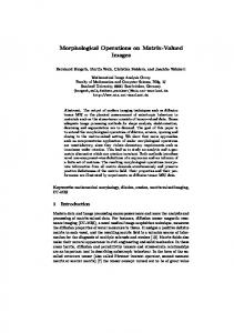
applications. However, we adopted Cell as a testbed architecture with the understanding that future variants for scientific computing will eventually include a fully pipelined double precision floating point unit and support for large virtual pages. This paper explores the complexity of mapping scientific algorithms to this chip architecture and uses simulation methods and analytic models to predict the potential performance of dense and sparse matrix arithmetic algorithms on Cell. We start with an overview of the Cell processor architecture. This is followed by a discussion of viable programming models. In the next section, the performance prediction methodology and simulation methods are introduced. Finally, we describe various methods for mapping dense and sparse matrix arithmetic to the Cell processor and predict their performance. The paper concludes with a glimpse into future explorations. 1. Cell Background Cell [1, 2] was designed by a partnership of Sony, Toshiba, and IBM (STI) to be the heart of Sony’s forthcoming PlayStation 3 gaming system. Cell takes a radical departure from conventional multiprocessor or multi-core architectures. Instead of using identical cooperating processors, it uses a conventional high performance PowerPC core that controls eight simple SIMD cores, or SPE’s. An overview of Cell is provided in Figure 1. 25.6 GB/s
PPC 512KB
memory controller
SPE 256KB
SPE 256KB
SPE 256KB
SPE 256KB
SPE 256KB
SPE 256KB
EIB 4 rings, 8bytes/ core cycle I/O
I/O
SPE 256KB
SPE 256KB
Figure 1 Cell Processor - Eight SPE’s, one PowerPC core, one memory controller, and two I/O controllers are connected via four rings. Each ring is 128b wide and runs at half the core frequency. Each SPE has its own local memory from which it runs programs.
Unlike a typical coprocessor, each SPE has its own local memory from which it fetches code and reads and writes data. The PowerPC core, in addition to virtual to physical address translation, is responsible for the management of the contents of each SPE’s 256KB of non-cache coherent local store. Thus to load and run a program on an SPE, the PowerPC core initiates the DMA’s of SPE program and data from DRAM to the local store. Once the DMA’s complete, the PowerPC core starts the SPE. For predictable data access patterns the local store approach is highly advantageous as it can be very efficiently utilized through explicit softwarecontrolled scheduling. Improved bandwidth utilization
through deep pipelining of memory requests, requires less power, and has a faster access time than a large cache due in part to its lower complexity. If however, the data access pattern lacks predictability, then the advantages of software managed memory are lost. Access to external memory is handled via a 25.6GB/s XDR memory controller. The PowerPC core, the eight SPE’s, the DRAM controller, and I/O controllers are all connected via 4 data rings, collectively known as the EIB. The ring interface within each unit allows 8 bytes/cycle to be read or written. Simultaneous transfers on the same ring are possible. All transfers are orchestrated by the PowerPC core. Each SPE includes four single precision 6-cycle pipelined FMA datapaths and one double precision halfpumped 9-cycle pipelined FMA datapath [20]. As more information becomes publicly available, these may need to be refined as sources are terse. Thus for computationally intense algorithms like GEMM, we expect single precision implementations to run near peak whereas double precision would drop to approximately one tenth the peak single-precision flop rate according to IBM’s design specifications [21]. Similarly, for bandwidth intensive applications – SpMV, we expect single precision to be between 50% and four times as fast depending on density and uniformity. 2. Programming Models Although the presence of eight independent processing elements offers huge benefits for peak performance, it presents a very challenging programming model. In this section, we explore some of the options available for mapping scientific algorithms onto this complex new architectural model. The data-parallel programming model is very common in the sciences and offers the simplest and most direct method of decomposing the problem. The programming model is very similar to loop-level parallelization afforded by OpenMP or the vector-like multistreaming on the Cray X1 and the Hitachi SR-8000. Although this decomposition offers the simplest programming model, the restrictions on program structure and the fine-grained synchronization mean that it may not be the fastest or the most efficient approach. If we adopt a more loosely coupled model, the same methods that are applied to partitioning problems for distributed memory machines can be applied to this processor as if it were a ”cluster on chip.” The DMA engines on the SPE’s can be used to mimic a messagepassing interface to coordinate action on the SPE’s. However, for some categories of algorithms, this model can become significantly more complicated than a dataparallel approach. A pipelined execution model was also envisioned by the Cell designers as a way to support streaming algorithms such as video codecs by partitioning stages of the process among the SPEs. However, we do not consider this programming model in this paper because early analysis indicated it did not present
significant benefits in easer of programming or performance over the other programming models. In each model, it is the responsibility of the PowerPC core to manage the flow of data in, out, and between the SPE’s. This management is very computationally light. Thus the PowerPC core, and most likely its L2 cache will be available for system functions without undermining computational performance or consuming much power. Each SPE is capable of simultaneously servicing DMA’s and executing code. Thus instead of loading data, computing on it, then returning the results before moving on to the next block – something analogous to bulk synchronous, the SPE’s should load data for the next operation, store data for the previous operation, and compute the current operation simultaneously. This of course necessitates double buffering inputs and outputs, and will incur a startup and finish overhead penalty like any pipelining approach. Nevertheless, in a data parallel approach, it should allow high utilization of either memory bandwidth or computational assets. 3. Simulation Methodology In this paper, performance estimation is broken into two steps commensurate with the two phase double buffered computational model. This provides a high level understanding of the performance limitations of the Cell processor on various algorithms. Once we gain access to a cycle accurate simulator, we will verify our results and gain understanding of the processor features that limit performance. In the first step, pencil and paper estimations were performed for operations such as gather, SAXPY, dot product, and register blocked matrix multiply. The resulting relations were quantified into models that took into account the SIMD nature of the SPE’s – i.e. 4 FLOPs/cycle vs. 1 FLOP/cycle at four times the frequency. In the second step, we construct a model that accounts for the time required to load, via DMA, various objects, such as vectors, matrix cache blocks, or a stream of nonzeros, into the local store of an SPE. The model must accurately reflect the constraints imposed by resource conflicts. For instance, a sequence of DMA’s issued to multiple SPE’s must be serialized, as there is only a single DRAM controller. The model also presumes a fixed DMA initiation latency of 1000 cycles based on existing design documents available regarding the Cell implementation. The model also presumes a broadcast mechanism that is similar to classic token ring network implementations where tokens are dispatched from the memory controller, travel along the ring as their data is copied by each SPE they pass, and are automatically removed once they have looped back to the memory controller. The width of the SIMD units, the number of SPE’s, and the local store size and bandwidth are encoded directly into the model as constants. External control is provided for parameters such as: the time for a SIMD
reduction, the steady state time (per element) for a gather, a dot product or a SAXPY, the time to perform an inter SPE vector reduction, and the DMA initiation latency. Our simulation framework is essentially a memory trace simulator – the difference being the complexity of the concurrent memory and computation operations that it must simulate. Instead of explicitly simulating computation using a cycle-accurate model of the functional units, we simulate the flow of data through the machine, and annotate the flow with execution time. The execution unit bandwidths and pipeline latencies are modeled as part of the data flow simulation. Therefore, our simulation is more sophisticated than a typical memory-trace simulator; however, it does not actually perform the computation. Additionally, instead of storing the matrix in a particular storage format and writing a program for each format, we store the key parameters for the matrix, and the nonzeros of the sparse matrix in an internal format, and write a performance annotator for each simulated storage format. This facilitated our work and allowed for detailed understanding of various characteristics of the sparse matrices. Each algorithm was broken into a number of phases in which communication for the current objects and computation for the previous objects can take place simultaneously. Of course, for each phase, it was necessary to convert cycles into actual time and FLOP rates. For simplicity we chose to model a 3.2GHz, 8 SPE version of Cell with 25.6GB/s of memory bandwidth which is likely to be used in the first release of the Sony PlayStation 3 [19]. This ensured that both the EIB and DRAM controller could deliver two single precision words per cycle. The maximum flop rate of such a machine would be 204.8GFLOP/s, with a computational intensity of 32 FLOPs/word. It is unlikely that any version of Cell would have less memory bandwidth or run at a lower frequency. For comparison, we use Cray’s X1 MSP and Intel’s Itanium2. The key characteristics of the processors are detailed in Table 1. CELL Chip multi-core
Architecture
SPE SIMD
Frequency DRAM BW GFLOP/s (single) GFLOP/s (double) Local Store L2 Cache L3 Cache Power
3.2GHz 25.6 2.6 256KB 3W [1]
3.2GHz 25.6GB/s 204.8 20.5 2MB 512KB ~30W
X1(MSP)
Itanium2
multi-chip Vector 800MHz 34GB/s 25.6 12.8 2MB 100W
VLIW 900MHz 6.4GB/s 3.6 3.6 256KB 1.5MB 130W
Table 1 Summary of architectural features of IBM’s Cell [21], the Cray X1 MSP, and Intel’s Itanium2 including single and double precision peak performance. A local store is not part of a cache hierarchy. Total Cell power is based on the active SPE’s/idle PowerPC programming model.
4. Dense Matrix Matrix Multiplication The first benchmark run, SGEMM, is a single precision dense matrix matrix multiply. With its extremely high computational intensity, one should expect Cell to achieve a high percentage of peak flop rate. Two storage formats were explored. The default is a column major format for all three matrices. The second format, block data layout, or BDL, organizes matrix sub-blocks into contiguous blocks of memory [7]. This can be particularly advantageous as it not only minimizes the number of DMA’s required, but also minimizes the number of pages touched when loading a sub-block. Although a matrix might not be stored in BDL, it can quickly be converted on the fly. Figure 2 shows a matrix stored in the two formats. 1 n+1
n
N
Figure 2 Left: column major layout. Right: BDL. Within each n x n block, values are stored in column major order
4.1 Algorithm Considerations Each matrix was broken into square “cache” blocks. Technically they aren’t cache blocks as the SPE’s have no caches, but for clarity we will continue to use the terminology. A column layout will require a number of short (cache block dimension) DMA’s equal to the dimension of the cache block – e.g. 64 DMA’s of length 64. BDL will require a single DMA of length 16KB. The assumed 1000 cycles of DMA latency can result in poor memory bandwidth usage for small cache blocks. The local store, being only 256KB, can’t store more than about 56K words of data because the program and stack must also fit in the local store. Cache blocks, if double buffered, require 6*n2 words of local store (one cache block from each matrix). Thus it is impossible, with the current version of Cell, to utilize square cache blocks larger than 96x96. Additionally, in column layout, there is additional pressure on the maximum cache block size for large matrices as each column within a cache block will be on a different page. Upward pressure is derived from the computational intensity of matrix multiplication and the FLOPs to word ratio of the processor. In the middle, there is a cache block size which delivers peak performance. The loop order in the column major storage format was chosen to minimize the average number of pages touched per phase. In BDL, as TLB misses are not nearly the problem, the loop order was chosen to minimize memory bandwidth. A data parallel approach was chosen to disseminate work between the SPE’s. Thus SPE cache
4.2 SGEMM Results Figure 3 shows SGEMM performance for various matrix dimensions, cache block sizes, and storage formats. Clearly shown is that 32x32 cache blocks are far too small to achieve a computational intensity high enough to fully utilize the processor. The choice of loop order and the resulting increase in memory traffic prevents column major 64x64 blocks from achieving 90% of peak. One doesn’t expect matrix multiplication to be memory bound, but for small cache blocks, it can be. Only 96x96 blocks provide enough computational intensity to overcome the additional block loads and stores. 204.8 179.2 153.6 GFLOP/s
1 N+1
blocks of size n x n are aggregated into Cell cache blocks of size 8n x n. An alternate approach considered, although not presented here would be to adapt Cannon’s algorithm [6] for parallel machines to a parallel machine on-chip. Although this could reduce the DRAM bandwidth requirements by transferring blocks via the EIB, for a column major layout, it could significantly increase the number of pages touched. Simulation based analysis will have to wait until a detailed model of the PowerPC TLB is available. For small matrix sizes, it is most likely advantageous to choose a model that minimizes the number of DMA’s. For example, broadcast both matrices, in their entirety, to all SPE’s.
128 102.4 76.8 51.2 25.6 0
N=256, N=2048, 32x32 32x32
N=512, 64x64
N=2048, 64x64
N=768, N=2304, 96x96 96x96
Matrix Dimension, Cacheblock Size
Column Major
BDL
Figure 3 SGEMM on Cell. Even with the minimum overhead of BDL, the lack of computational intensity prevents 32x32 cache blocks from attaining 60% of peak. The inefficiency of column major layout prevents it from reaching peak performance without very large cache blocks.
It should be noted that if the DMA latency were 100 cycles, then the 64x64 column major performance would reach parity with BDL. This is certainly a motivation for user controlled DMA. Alternatively, if 128x64 blocks were used, then performance would also rival BDL. Higher frequencies (e.g. 4GHz) will not help if peak performance is not being achieved due to high memory traffic, DMA latency, or TLB misses. Similarly,
higher bandwidth will go unused if the configuration is computationally bound. Larger local stores, and thus larger cache blocks are not necessarily helpful in the column major layout as that would necessitate more pages being touched, and the likelihood of far more TLB misses. This is not an obstacle in the BDL approach. 4.3 DGEMM Results A similar set of strategies and simulations were performed for DGEMM. Cache blocks are now limited to be no larger than 64x64 – finite local store. This is not the performance limitation it was in SGEMM. Although the time to load a double precision 64x64 cache block is twice that of a single precision version, the time required to compute on a 64x64 double precision cache block is about ten times (no more fully pipelined SIMD) as long as the single precision counterpart. Thus it is far easier for double precision to reach its peak performance. Of course peak double precision performance is one tenth of single precision – a mere 20 GFLOP/s. 4.4 Comparison At 3.2GHz, each SPE requires about 3W [1]. Thus with a nearly idle PPC and L2, Cell achieves over 200GFLOP/s for around 30W – nearly 7GFLOP/s/W. Clearly Cell is highly efficient at large matrix multiplication DGEMM and SGEMM were also run on Cray’s X1, and a 900MHz Itanium2. The results are detailed in the Table 2.
Peak
Double (GFLOP/s) Cell X1 Itanium2 20.4 11.2 3.5
Single (GFLOP/s) Cell X1 Itanium2 204.7 16.4 3.6
Table 2 Peak GEMM performance (in GFLOP/s) for large square matrices on Cell, X1, and the Itanium2. With about ¼ the power, Cell is nearly 6 times faster in double precision and more than 50 times faster in single precision than the Itanium2.
The 900MHz Itanium2 is capable of running the Intel MKL DGEMM at 3.5GFLOP/s. Although this number is an impressively high percentage of peak, the architecture is not power efficient, and scaling to multiprocessors exacerbates the problem. For example a 4 processor 1.5GHz Itanium2 system will consume well over 500W, and yet only deliver about 22GFLOP/s. Contrast this with a single Cell processor which consumes less than 1/15th the power and provides about the same performance in double precision – by no means Cell’s forte. The Itanium2 does not have SIMD support. Thus, in single precision, Cell is more than 100 times more power efficient. Similarly, in double precision, Cell is about twice as fast as the X1, and at least 6 times more power efficient. In single precision, Cell is nearly 40 times more power efficient.
The primary focus for matrix multiplication on Cell is the choice of data storage to minimize the number of DMA’s and TLB misses while maximizing computational intensity. Secondary is the choice of programming model. The decoupling of main memory data access from the computational kernel guarantees constant memory access latency since there will be no cache misses, and all TLB accesses are resolved in the communication phase. Matrix multiplication is perhaps the best benchmark to demonstrate Cell’s computational capabilities as it achieves high performance by buffering large cache blocks on chip before computing on them
5. Sparse Matrix Vector Multiply Naïvely, SpMV would seem to be the worst application to run on Cell since the SPE’s have neither caches nor gather/scatter support. Furthermore, SpMV has O(1) computational intensity. However, these are perhaps less important than the low functional units and local store latency (