APPLIED PHYSICS LETTERS 93, 081113 共2008兲
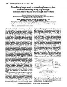
Dense wavelength conversion and multicasting in a resonance-split silicon microring Qiang Li,1 Ziyang Zhang,2 Fangfei Liu,1 Min Qiu,2,a兲 and Yikai Su1,b兲 1
State Key Laboratory of Advanced Optical Communication Systems and Networks, Department of Electronic Engineering, Shanghai Jiao Tong University, Shanghai 200240, China 2 Laboratory of Optics, Photonics and Quantum Electronics, Department of Microelectronics and Applied Physics, Royal Institute of Technology (KTH), Electrum 229, 164 40 Kista, Sweden
共Received 27 May 2008; accepted 6 August 2008; published online 27 August 2008兲 We experimentally demonstrate all-optical wavelength conversions in a 10 m radius resonance-split silicon microring resonator based on free carrier dispersion effect. The split resonance is caused by the mutual coupling between the two countertraveling modes inside the ring resonator. Dense wavelength conversions are performed at data rates from 500 Mbytes/s to 5 Gbytes/s and a dual-channel wavelength multicasting is realized at a data rate of 1.25 Gbytes/s. The resonance splitting phenomenon opens up opportunities to convert more closely spaced wavelengths, thus effectively increasing the system capacity. © 2008 American Institute of Physics. 关DOI: 10.1063/1.2976123兴 Wavelength conversion is an important function for alloptical networks to alleviate the data blocking due to wavelength contention in the dynamic, high-capacity wavelengthdivision-multiplexed 共WDM兲 networks.1 The all-optical wavelength converter is regarded as a promising alternative to optical-electronic-optical wavelength conversion.2 It has been demonstrated in a variety of media, such as highly nonlinear fibers,3 semiconductor optical amplifiers,4 periodically poled lithium niobate crystals,5 and GaAs microring resonators.6 Recently, silicon-on-insulator 共SOI兲 nanophotonic waveguides, i.e., silicon wires, have attracted much attention due to their compact sizes and compatibility with the complementary metal oxide semiconductor fabrication. The wavelength conversions have been demonstrated in silicon straight waveguides by exploiting four-wave mixing7,8 and in silicon ring resonators based on the free carrier dispersion 共FCD兲 effect and resonance shift.9 The use of a microring resonator with a high quality factor can compensate the weak nonlinearity of the miniaturized silicon devices and thus relax the power requirement. For the wavelength conversion based on the FCD effect in a silicon ring resonator, a pump light and a signal light are required, where they work at different resonances. The signal light is usually a continuous wave 共cw兲. In the previous reports, however, the pump and signal resonances are separated by at least one free space range 共FSR兲.9 For the smallradius ring resonator in SOI, the FSR is usually large, thus limiting the choices of wavelengths/channels that can be adopted for the conversion. A conventional microring with a FSR below 1 nm requires a diameter of a few 100 m.10 For a ring resonator side coupled to a waveguide, if periodic roughness 共grating兲 on the sidewall of the ring is introduced, both propagating and counterpropagating modes can be excited.11 The induced resonance splitting eliminates the need of separating the pump and signal by at least a FSR and enables more channels for conversions, thus significantly increasing the system capacity. In this paper, we demonstrate
high-speed dense wavelength conversion and dual-channel wavelength multicasting, based on the FCD effect in the resonance-split silicon microring resonator. As shown in Ref. 11, the resonance splitting is caused by the mutual coupling between the modes inside the ring resonator. The incident wave si only generates the counterclockwise traveling mode a, which in turn induces the counterpropagating mode b due to the grating that is present along the ring sidewalls, as shown in Fig. 1. Modes a and b are related by the mutual coupling factor Qu. Considering the degenerate case, modes a and b have the same resonance frequency 0, intrinsic quality factor Qi, and coupling quality factor Qe. The transmission function of the ring resonator is given by
0 st =1− si 2Qe
+
冉
冤冉
1
j − 0 +
j − 0 −
1
冊
冊
0 0 0 + + 2Qu 2Qi 2Qe
0 0 0 + + 2Qu 2Qi 2Qe
冥
.
共1兲
It can be seen that mode a is split into two resonance frequencies, namely, 0 − 0 / 共2Qu兲 and 0 + 0 / 共2Qu兲. Therefore, the splitting separation is solely determined by the mutual coupling factor Qu. The microring resonator used in the experiments is fabricated on a commercial single-crystalline SOI wafer with a 250-nm-thick silicon slab on top of a 3 m silica buffer layer. The radius of the ring is 10 m. The ring/waveguide cross section is 450⫻ 250 nm2 with an effective area of
a兲
Electronic mail:
[email protected]. Electronic mail:
[email protected].
b兲
0003-6951/2008/93共8兲/081113/3/$23.00
FIG. 1. Schematic of a ring resonator side coupled to a waveguide. 93, 081113-1
© 2008 American Institute of Physics
Author complimentary copy. Redistribution subject to AIP license or copyright, see http://apl.aip.org/apl/copyright.jsp
081113-2
Li et al.
Appl. Phys. Lett. 93, 081113 共2008兲
FIG. 2. The SEM photos of 共a兲 the silicon microring resonator with a radius of 10 m and 共b兲 the grating on the sidewall of the ring resonator. Inset in 共a兲 is a zoom-in view of the coupling region.
about 0.1 m2 for the transverse-electric 共TE兲 mode. The microring is side coupled to the straight waveguide with an air gap of 120 nm. The waveguide and ring patterns are first defined in the e-beam lithography and transferred to the top silicon layer by reactive ion plasma etching. The waveguide is slowly tapered to a width of 10 m at both ends, where gold gratings are added to couple light near vertically from single mode fibers.12 The grating couples only TE light with a minimal fiber-to-fiber loss below 20 dB. The scanning electron microscope 共SEM兲 photo of the silicon microring resonator is provided in Fig. 2共a兲. Figure 2共b兲 shows the grating on the ring sidewall. The width of the grating ridge is ⬃20 nm and the period ranges from ⬃50 to ⬃100 nm. They are determined by a variety of parameters during the e-beam process, namely, the scan step size, line scan intervals, exposure dose, and developing time, which have been detailed in Ref. 11. Figure 3 shows the spectral response of the ring resonator. The notches around 1550 nm are fitted using Eq. 共1兲. The obtained intrinsic Qi, coupling Qe, and mutual coupling Qu are 6.5⫻ 104, 2.0⫻ 104, and 3.7⫻ 103, respectively, indicating a strong mutual coupling and thus resonance splitting. The experimental setup is depicted in Fig. 4. The pump wavelength p1 is chosen to offset the thermal nonlinear effect. The signal wavelength 1 is fixed at the left resonance for the noninverted case and 2 at the shorter wavelength edge of the left resonance for the inverted case. A Mach– Zehnder modulator, driven by an electrical pseudorandom bit sequence signal of 27 − 1 pattern length, is used to generate non-return-to-zero signal. The pump light is boosted by a high power erbium doped fiber amplifier 共EDFA兲 followed by an attenuator to adjust the pump power. The pump light and the signal light are combined through a 90:10 coupler and launched into the microring resonator by the vertical
FIG. 3. 共Color online兲 The transmission spectrum demonstrating the resonance splitting effect.
FIG. 4. Experimental setup. Pulse pattern generator.
coupling system. The output signal of the microring resonator is amplified using two cascaded EDFAs, each followed by a ⬃0.3 nm bandpass filter to separate the signal from the pump, and then sent to an oscilloscope to record the waveforms. As the gold grating coupler is polarization dependent, two polarization controllers are inserted before the coupler to make sure that the input pump and signal lights are in TE mode. The pump power into the input of the waveguide is ⬃7.7 dBm and the signal power is ⬃−4 dBm at the input of the fiber. Figure 5 shows the dense wavelength conversion results
FIG. 5. 共Color online兲 Dense wavelength conversions at 500 Mbytes/s, 1 Gbyte/s, 2 Gbytes/s, and 5 Gbytes/s. The horizontal axes represent the time 共ns兲 and the vertical axes represent the normalized intensity.
Author complimentary copy. Redistribution subject to AIP license or copyright, see http://apl.aip.org/apl/copyright.jsp
081113-3
Appl. Phys. Lett. 93, 081113 共2008兲
Li et al.
FIG. 6. 共Color online兲 Dual-channel wavelength multicasting at 1.25 Gbytes/s. The horizontal axes represent the time 共ns兲 and the vertical axes represent the normalized intensity.
for data rates of 500 Mbytes/s, 1 Gbyte/s, 2 Gbytes/s, and 5 Gbytes/s. Both noninverted and inverted waveforms are provided. With the signal wavelength at 1, the transmission of the signal light increases when the carriers are generated and the resonances are blueshifted, resulting in a noninverted conversion, as shown on the left of Fig. 5. With the signal wavelength at 2, the transmission of the signal light decreases when the resonances are blueshifted, resulting in an inverted conversion, shown on the right of Fig. 5. As the bit rate increases, the extinction ratio for the converted signal is reduced, mainly resulting from the long carrier lifetime.13 The carrier lifetime induces a lower extinction ratio for the single “1’s” since they have much shorter rise time and falling time compared to the consecutive 1’s and thus cannot respond to the pump signal rapidly. According to the equation in Ref. 9, the resonance shift of a 3 dB bandwidth of the ring resonator corresponds to an effective index change of ⬃1.5⫻ 104. The calculated required pump power is ⬃8 dBm. We also demonstrate a dual-channel wavelength multicasting, which is needed in the WDM-based all-optical network.14 In this process, the input signal is converted into two output wavelengths simultaneously. The locations of converted signal wavelengths are shown in Fig. 3. Another cw laser is used in this experiment and the pump is set at the resonance across a FSR 共⬃1564 nm兲 with respect to the
converted signal wavelength, which shows a notch depth of ⬃25 dB and a bandwidth of ⬃0.075 nm. Figures 6共b兲 and 6共c兲 represent the noninverted dual-channel wavelength multicasting at 1.25 Gbytes/s, while Figs. 6共d兲 and 6共e兲 demonstrate the inverted case. For intrinsic silicon, the carrier lifetime limits the available operation speed. The carrier lifetime can be greatly reduced by using a reverse-biased p-i-n junction15 or by ion implantation.16,17 The pump power needed for wavelength conversion can be further reduced by fabricating ring resonators with much higher Q factors, by employing smaller radius and by improving the efficiency of the fiber-towaveguide coupling. To summarize, we have demonstrated the dense wavelength conversion and dual-channel wavelength multicasting in a silicon microring resonator with resonance splitting, which is caused by the mutual coupling between the two modes inside the ring. The resonance splitting in silicon microring resonators opens up opportunities to convert more wavelengths that are densely spaced and effectively increases the system capacity. This work is supported by the National Natural Science Foundation of China 共Grant No. 60777040兲, the Shanghai Rising Star Program Phase II 共Grant No. 07QH14008兲, the Swedish Foundation for Strategic Research, and the Swedish Research Council. S. J. B. Yoo, J. Lightwave Technol. 14, 955 共1996兲. S. L. Danielsen, P. B. Hansen, and K. E. Stubkjaer, J. Lightwave Technol. 16, 2095 共1998兲. 3 K. Inoue and H. Toba, IEEE Photon. Technol. Lett. 4, 69 共1992兲. 4 T. Durhuus and B. Mikkelsen, J. Lightwave Technol. 14, 942 共1996兲. 5 J. Yamawaku, H. Takara, T. Ohara, K. Sato, A. Takada, T. Morioka, O. Tadanaga, H. Miyazawa, and M. Asobe, Electron. Lett. 39, 1144 共2003兲. 6 P. P. Absil, J. V. Hryniewicz, B. E. Little, P. S. Cho, R. A. Wilson, L. G. Joneckis, and P. T. Ho, Opt. Lett. 25, 554 共2000兲. 7 H. Rong, Y. H. Kuo, A. Liu, M. Paniccia, and O. Cohen, Opt. Express 14, 1182 共2006兲. 8 M. A. Foster, A. C. Turner, R. Salem, M. Lipson, and A. L. Gaeta, Opt. Express 15, 12949 共2007兲. 9 Q. Xu, V. R. Almeida, and M. Lipson, Opt. Lett. 30, 2733 共2005兲. 10 P. Dong, S. F. Preble, and M. Lipson, Opt. Express 15, 9600 共2007兲. 11 Z. Zhang, M. Dainese, L. Wosinski, and M. Qiu, Opt. Express 16, 4621 共2008兲. 12 S. Scheerlinck, J. Schrauwen, F. V. Laere, D. Taillaert, D. V. Thourhout, and R. Baets, Opt. Express 15, 9625 共2007兲. 13 V. R. Almeida, C. A. Barrios, R. R. Panepucci, and M. Lipson, Nature 共London兲 431, 1081 共2004兲. 14 R. K. Pankaj, IEEE/ACM Trans. Netw. 7, 414 共1999兲. 15 S. F. Preble, Q. Xu, B. S. Schmidt, and M. Lipson, Opt. Lett. 30, 2891 共2005兲. 16 M. Först, J. Niehusmann, T. Plötzing, J. Bolten, T. Wahlbrink, C. Moormann, and H. Kurz, Opt. Lett. 32, 2046 共2007兲. 17 M. Waldow, T. Plötzing, M. Gottheil, M. Först, J. Bolten, T. Wahlbrink, and H. Kurz, Opt. Express 16, 7693 共2008兲. 1 2
Author complimentary copy. Redistribution subject to AIP license or copyright, see http://apl.aip.org/apl/copyright.jsp