138
Journal of Power Electronics, Vol. 10, No. 2, March 2010
JPE 10-2-5
Design and Application of a Single Phase Multilevel Inverter Suitable for using as a Voltage Harmonic Source Ersoy Beser† , Birol Arifoglu∗ , Sabri Camur∗ , and Esra Kandemir Beser∗ †∗ Dept.
of Electrical Eng., Kocaeli University, Kocaeli, Turkey
Abstract This paper presents a single phase multilevel inverter for using as a voltage harmonic source. First, a single phase multilevel inverter system is presented and the structural parts of the inverter are described. In order to obtain multilevel output voltage waveforms, a switching strategy based on calculating switching angles is explained and an improved formula for determining switching angles is given. Simulation and experimental results of multilevel voltage waveforms are given for 15, 31 and 127 levels. The proposed topology does not only produce output voltages with low THD values. It also produces the required harmonic components on the output voltage. For this purpose, equations for switching angles are constituted and the switching functions are obtained. These angles control the output voltage as well as provide the required specific harmonics. The proposed inverter structure is simulated for various functions with the required harmonic components. The THD values of the output voltage waves are calculated. The simulated functions are also realized by the proposed inverter structure. By using a harmonic analyzer, the harmonic spectrums, which belong to the output voltage forms, are found and the THD values are measured. Simulation and experimental results are given for the specific functions. The proposed topology produces perfectly suitable results for obtaining the specific harmonic components. Therefore, it is possible to use the structure as a voltage harmonic source in various applications. Key Words: Harmonic, Harmonic components, Harmonic source, Multilevel inverter, Voltage active filter
NOMENCLATURE Vd Vmax Vref V0 Vf Vh Vdc n m r θj ϕh ω tmax tsample ff Q(k−1)
voltage of the first level module maximum value of the required load voltage reference voltage output voltage peak voltage of the fundamental harmonic component peak voltage of the hth harmonic component dc component value of the output voltage number of output voltage levels number of level modules number of switches switching angle phase angle angular speed maximum value of the sample time value of the sample time frequency of the fundamental harmonic component (k − 1)th switching signal
Manuscript received Oct. 16, 2009; revised Jan. 14, 2010 † Corresponding Author:
[email protected] Tel: +902623033490, Kocaeli University ∗ Dept. of Electrical Eng., Kocaeli University, Turkey
I. I NTRODUCTION Power electronic inverters have been used in various applications recently. Inverters have become a necessity for many implementations in industrial areas. So, numerous configurations and switching strategies have been presented and discussed extensively. Particularly, multilevel inverters have received increasing interest for power conversion in high-power applications due to their lower harmonics, higher efficiency and lower voltage stress compared to two-level inverters [1]. Various topologies for multilevel inverters have been introduced and widely studied [1]– [23]. The most considerable of these topologies are the diode clamped [neutral-point clamped (NPC)] inverter [7], the capacitor clamped (flying capacitor) inverter [8] and the cascaded H-bridge inverter with separated dc sources [9]. Multilevel inverters generate a staircase waveform. By increasing the number of output levels, the output voltages have more steps and harmonic content on the output voltage and the THD values are reduced [10]. Therefore, they produce highquality output voltage by increasing the level number. However, in some conditions, the harmonic components on an output voltage wave are required for special applications. For example harmonic components are needed for researching the effects of harmonic components on transformers, induction machines, capacitors and they are used in transmission lines to observe their results. Specific harmonic components are also
139
Design and Application of a Single Phase Multilevel Inverter Suitable for · · ·
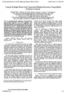
Fig. 2.
Fig. 1.
Configuration of the proposed single phase multilevel inverter system for 15 levels.
required for voltage active filter applications. This paper presents the performance of a single phase multilevel inverter for using as a voltage harmonic source. The structure of the proposed inverter is different from some inverter types in literature [11]. The level number can be easily increased. As a result, voltage stress is reduced and more sinusoidal shaped output voltage waves can be obtained. In addition, the required harmonic components on an output voltage wave can be obtained suitably for the objectives of this study. To accomplish this, a method for finding the switching equations is explained. The proposed inverter is simulated for various specific functions including harmonic content. The validity of the proposed method is verified through an experimental study. The proposed inverter gives perfect performance for obtaining the required harmonic components. Therefore, its use as a voltage harmonic source is highly efficient. II. P ROPOSED M ULTILEVEL I NVERTER S YSTEM A ND S WITCHING S TRATEGY F OR M ULTILEVEL VOLTAGE WAVES In this study, a single phase multilevel inverter system is proposed. The principle of the proposed method will be explained for a 15-level inverter. However, the structure can be easily adapted to any number of levels. The configuration of the inverter structure is shown in Fig.1. The proposed multilevel inverter structure consists of two basic parts. The parts are classified as Level and H-Bridge Modules. The most remarkable feature of the system is its ease of expansion. By increasing the number of level modules and connecting them cascaded, the inverter system can expand and the voltage level number can be easily increased. The Level Module consists of two semiconductor switching devices and a dc source. The voltage of the dc source is expressed by k and Vd as 2(k−1) ·Vd . Generally Vd is expressed as: 2 · Vmax Vd = (1) n−1 k=1, 2, 3, . . . , m. (2)
15-level output voltage (V0 ), reference voltage wave (VRef ) and switching angles (θ1 , θ2 , θ3 ,. . . θ7 ).
The number of switches and output levels related to the number of cascaded level modules are given in Table 1. As it can be seen from Table 1, in the event of using four level modules, a 31-level output voltage form is obtained. However this level number is the maximum value for four level modules. By using four level modules in the inverter structure, 17, 19, 21,. . . ,29-level voltage waves can be obtained addition to the 31-level output. Therefore, the output level numbers in the table are the maximum values for the given level module number. TABLE I N UMBER OF SWITCHES AND OUTPUT LEVELS RELATED TO NUMBER OF CASCADED LEVEL MODULES (L M ) Cascaded
DC Source
Output Level (n)
Level Modules
Ratio
LM1
1Vd
Number of Switches (r) 3
LM2
2Vd
LM3
4Vd
LM4
8Vd
LM5
16Vd
LM6
32Vd
: :
: :
LM m
2(m−1) Vd
6 7 8 15 10 31 12 63 14 127 16 : : 2(m+1) − 1 2m + 4
The number of output level (n) and the number of switches (r) are expressed as follows: n= 2(m+1) − 1
(3)
r = 2m + 4.
(4)
The switching strategy in the proposed method is to generate gate signals by calculating switching angles [20]. The required switches are switched alternately and multilevel output voltage wave is obtained by using the calculated angle values and the known frequency. For calculating switching angles, a simple method is developed for the proposed inverter topology. The
140
Journal of Power Electronics, Vol. 10, No. 2, March 2010
Fig. 3.
(a) Simulation, 15-level
(b) Experimental, 15-level
(c) Simulation, 31-level
(d) Experimental, 31-level
(e) Simulation, 127-level
(f) Experimental, 127-level
Simulation and experimental results of multilevel output voltage (V0 ) for resistive loads in the proposed multilevel inverter.
formula for this method is given as follows: 2j − 1 θj = sin−1 n− 1 n − 1 . j = 1, 2, 3, . . . , 2
(5) (6)
For instance, the switching angles θ1 , θ2 , θ3 , θ4 , θ5 , θ6 and θ7 can be calculated by using equations (5) and (6) for a single phase 15-level inverter topology. The output voltage and the reference voltage waves according to the calculated switching angles are illustrated in Fig.2 for a 15-level topology. In order to increase the output voltage levels, level modules are increased and various output levels can be obtained in respect to equation (3). This approach can be easily applied to any number of levels. In this case, switching angles should be calculated for each voltage level number. In Fig.3 simulation and experimental results of output voltage waves in the proposed multilevel inverter are given for 15, 31 and 127-level voltage waveforms.
The output voltages can have more steps by increasing the number of output levels. In this condition, the shape of output voltage converges more to a sinusoidal waveform and the THD value of output voltage is considerably reduced. Through simulations and experiments, it can be seen that the proposed inverter topology generates a high-quality output voltage waveform. By increasing the level number, the THD values of the output voltage decrease even for resistive loads. The switching strategy is simple and switching angles can be easily obtained by using the formula. The ease of expansion for the proposed multilevel inverter system makes it easy to increase the number of output levels. By increasing the level number and producing a multilevel voltage wave, dv/dt stresses imposed on power-switching devices are reduced in the proposed topology. III. D ETERMINING S WITCHING A NGLES F OR O BTAINING H ARMONIC C OMPONENTS The proposed multilevel inverter produces multilevel output voltages with low harmonic content as mentioned in section
Design and Application of a Single Phase Multilevel Inverter Suitable for · · ·
Fig. 4.
Fig. 5.
A sample reference output voltage wave.
141
Switching signals in the proposed multilevel inverter including four level modules.
2. The proposed structure is also capable of producing the required harmonic components on the output voltage so that it can be used as a voltage harmonic source. In order to obtain an output voltage with harmonic content, first, the required harmonic components are determined and the equation for the reference voltage is obtained as follows: ∞
Vref =
Vdc X Vh sin(hωt + ϕh ). + 2
(7)
h=1
In equation (8), a sample reference function is given and the output voltage wave of the sample function is illustrated in Fig.4. Vref = V1 sin ωt + V3 sin 3ωt.
Output voltage of the proposed multilevel inverter including four level modules.
Fig. 7.
Output voltage of the proposed multilevel inverter including five level modules.
(8)
∆t seen in Fig.4 gives the sample time of switching signals. When a smaller value is chosen, the output voltage more closely resembles the reference signal. The sample time is related to the frequency of the fundamental harmonic component and the level module number. In equation (9) the maximum value of sample (tmax ) time, which is related to the fundamental frequency and the level module number, is given. During operation, the sample time (tsample ) should be chosen smaller than tmax for obtaining an output voltage that is similar to the reference signal. 1 · (2πff )−1 tmax = sin−1 (9) 2(m+1) − 2 tsample = ∆t = ti+1 − ti (10) tsample