Aug 5, 2008 - Calorimeter for the International Linear Collider ... University of Birmingham, School of Physics and Astronomy, ... Prague 8, Czech Republic.
draft v4.4
arXiv:0805.4833v2 [physics.ins-det] 5 Aug 2008
Preprint typeset in JINST style - HYPER VERSION
Design and Electronics Commissioning of the Physics Prototype of a Si-W Electromagnetic Calorimeter for the International Linear Collider
The CALICE Collaboration J.Repond Argonne National Laboratory, 9700 S. Cass Avenue, Argonne, IL 60439-4815, USA J.Yu University of Texas, Arlington, TX 76019, USA C.M.Hawkes, Y.Mikami, O.Miller, N.K.Watson, J.A.Wilson University of Birmingham, School of Physics and Astronomy, Edgbaston, Birmingham B15 2TT, UK G.Mavromanolakis, M.A.Thomson, D.R.Ward, W.Yan University of Cambridge, Cavendish Laboratory, J J Thomson Avenue, CB3 0HE, UK F.Badaud, D.Boumediene, C.Cârloganu, R.Cornat, P.Gay, Ph.Gris, S.Manen, F.Morisseau, L.Royer Laboratoire de Physique Corpusculaire de Clermont-Ferrand (LPC), 24 avenue des Landais, 63177 Aubière CEDEX, France G.C.Blazey, D.Chakraborty, A.Dyshkant, K.Francis, D.Hedin, G.Lima, V.Zutshi NICADD, Northern Illinois University, Department of Physics, DeKalb, IL 60115, USA J.-Y.Hostachy, L.Morin Laboratoire de Physique Subatomique et de Cosmologie, Université Joseph Fourier (Grenoble 1), 53, av. des Martyrs, 38026 Grenoble CEDEX, France E.Garutti, V.Korbel, F.Sefkow DESY, Notkestrasse 85, D-22603 Hamburg, Germany M.Groll Univ. Hamburg, Physics Department, Institut für Experimentalphysik, Luruper Chaussee 149, 22761 Hamburg, Germany G.Kim, D-W.Kim, K.Lee, S.Lee Kangnung National University, HEP/PD, Kangnung, South Korea K.Kawagoe, Y.Tamura Department of Physics, Kobe University, Kobe, 657-8501, Japan
–1–
D.A.Bowerman, P.D.Dauncey, A.-M.Magnan, C.Noronha, H.Yilmaz, O.Zorba Imperial College, Blackett Laboratory, Department of Physics, Prince Consort Road, London SW7 2BW, UK V.Bartsch, J.M.Butterworth, M.Postranecky, M.Warren, M.Wing Department of Physics and Astronomy, University College London, Gower Street, London WC1E 6BT, UK M.Faucci Giannelli, M.G.Green, F.Salvatore, T.Wu Royal Holloway University of London, Dept. of Physics, Egham, Surrey TW20 0EX, UK D.Bailey, R.J.Barlow, M.Kelly, S.Snow, R.J.Thompson The University of Manchester, School of Physics and Astronomy, Schuster Lab, Manchester M13 9PL, UK M.Danilov, V.Kochetkov Institute of Theoretical and Experimental Physics, B. Cheremushkinskaya ul. 25, RU-117218 Moscow, Russia N.Baranova, P.Ermolov, D.Karmanov, M.Korolev, M.Merkin,A.Voronin M.V. Lomonosov Moscow State University (MSU), Faculty of Physics, Leninskiye Gory, Moscow, 119992, Russia B.Bouquet, S.Callier, F.Dulucq, J.Fleury, H.Li, G.Martin-Chassard, F.Richard, Ch.de la Taille, R.Poeschl, L.Raux, M.Ruan, N.Seguin-Moreau, F.Wicek, Z.Zhang Laboratoire de L’accélerateur Linéaire, Centre d’Orsay, Université de Paris-Sud XI, BP 34, Bâtiment 200, F-91898 Orsay CEDEX, France M.Anduze, V.Boudry, J-C.Brient, C.Clerc, G.Gaycken, C.Jauffret, A.Karar, P.Mora de Freitas, G.Musat, M.Reinhard, A.Rougé, A.L.Sanchez, J-Ch.Vanel, H.Videau École Polytechnique, Laboratoire Leprince-Ringuet (LLR), Route de Saclay, F-91128 Palaiseau, CEDEX France J.Zacek Charles University, Institute of Particle & Nuclear Physics, V Holesovickach 2, CZ-18000 Prague 8, Czech Republic J.Cvach, P.Gallus, M.Havranek, M.Janata, M.Marcisovsky, I.Polak, J.Popule, L.Tomasek, M.Tomasek, P.Ruzicka, P.Sicho, J. Smolik, V.Vrba, J.Zalesak Institute of Physics, Academy of Sciences of the Czech Republic, Na Slovance 2, CZ-18221 Prague 8, Czech Republic Yu.Arestov Institute of High Energy Physics, Moscow Region, RU-142284 Protvino, Russia A.Baird, R.N.Halsall Rutherford Appleton Laboratory, Chilton, Didcot, Oxon OX110QX, UK S.W.Nam, I.H.Park, J.Yang Ewha Womans University, Dept. of Physics, Seoul 120, South Korea
–2–
A BSTRACT: The CALICE collaboration is studying the design of high performance electromagnetic and hadronic calorimeters for future International Linear Collider detectors. For the electromagnetic calorimeter, the current baseline choice is a high granularity sampling calorimeter with tungsten as absorber and silicon detectors as sensitive material. A “physics prototype” has been constructed, consisting of thirty sensitive layers. Each layer has an active area of 18 × 18 cm2 and a pad size of 1 × 1 cm2 . The absorber thickness totals 24 radiation lengths. It has been exposed in 2006 and 2007 to electron and hadron beams at the DESY and CERN beam test facilities, using a wide range of beam energies and incidence angles. In this paper, the prototype and the data acquisition chain are described and a summary of the data taken in the 2006 beam tests is presented. The methods used to subtract the pedestals and calibrate the detector are detailed. The signal-overnoise ratio has been measured at 7.63 ± 0.01. Some electronics features have been observed; these lead to coherent noise and crosstalk between pads, and also crosstalk between sensitive and passive areas. The performance achieved in terms of uniformity and stability is presented. K EYWORDS : Calorimeters;Detector alignment and calibration methods;Detector design and construction technologies and materials.
Contents 1.
ECAL Si-W physics prototype 1.1 Physics considerations driving the design 1.2 Geometry and mechanical structure 1.2.1 Fabrication processes 1.2.2 Beam test configurations 1.3 Description of the sensitive area 1.3.1 Module test setup and results 1.3.2 Calibration of the slabs
2.
Electronics and data acquisition 2.1 On-detector readout electronics 2.1.1 FLC_PHY3 ASIC 2.1.2 Power consumption 2.1.3 Very Front End boards 2.2 Off-detector electronics 2.2.1 Implementation 2.2.2 Trigger and timing 2.2.3 Performance 2.2.4 Readout software
8 9 9 11 11 11 12 12 13 13
3.
Beam tests 3.1 Beam lines at DESY and CERN in 2006 3.2 Summary of the data collected
14 14 15
4.
Pedestal, noise, and crosstalk around module edge 4.1 Pedestal subtraction procedure 4.1.1 VFE PCB-wise correlated pedestal shifts 4.1.2 Correlated noise and signal-induced pedestal shift 4.2 Uniformity and stability of the residual pedestals and noise 4.2.1 Uniformity and stability of the residual pedestals 4.2.2 Uniformity and stability of the noise 4.2.3 Conclusion 4.3 Crosstalk around the module edge
17 17 17 19 20 20 22 23 24
5.
Calibration of the detector 5.1 Extraction of the calibration constants per channel 5.2 Results 5.2.1 Uniformity across the detector 5.2.2 Stability in time 5.2.3 Summary
25 26 27 28 28 30
–1–
2 2 3 4 5 6 7 8
1. ECAL Si-W physics prototype The CALICE (Calorimetry for the Linear Collider Experiments) collaboration [1] is studying several designs of calorimeters for experiments at the future International Linear Collider (ILC) [2]. In order to have a mature design when the first results from the Large Hadron Collider experiments are expected and decisions on future colliders made, two main development phases have been defined. In the first phase, characterised by the construction of “physics prototypes”, the feasibility of building a pixelised calorimeter is studied. In the second phase, “technological prototypes” will focus on the engineering details needed to insert such a calorimeter in an ILC detector. In both phases, the prototypes will be subject to extensive studies at beam test facilities. The data acquisition (DAQ) chain is common to all calorimeters, thereby easing their integration. The physics prototype for the electromagnetic calorimeter (ECAL) described in this document is a high granularity silicon-tungsten sampling calorimeter. Whereas the proof-of-principle of such detector has already been proven e.g. at LEP [3] [4] and SLD [5], the challenge for an ILC detector is the much larger size and the compactness required. Physics at the ILC places stringent requirements on the detector [2], including the ability to p measure jet energies with a precision of at least 0.3/ Ejj /GeV 1 . It has been demonstrated in Monte Carlo (MC) simulations [6] that the Particle Flow Algorithm (PFA) [7] approach to the reconstruction of jet energies in terms of the individual particles can achieve this goal for typical jets at the ILC. The next step is to validate these MC simulations by testing real scale prototypes in beam tests. For an ILC detector, the ECAL has to be as compact as possible, in order to achieve the smallest possible effective Molière radius and to reduce the cost of the surrounding magnet. In addition, high transverse and longitudinal segmentation is required for the PFA to be effective. 1.1 Physics considerations driving the design With a sampling calorimeter approach, the choice of absorber material is driven by the need to separate particles in a jet and the need for a compact calorimeter. Separation of particles in the transverse direction requires an absorber material which gives narrow electromagnetic (EM) showers and so needs to have a small Molière radius. Separation longitudinally requires a material with short EM showers, which pushes for a material with a small radiation length (X0 ). The same requirement also results in a compact ECAL. Tungsten is such a material, with a Molière radius of 9 mm, and a radiation length of 3.5 mm. Furthermore, the ratio of interaction length to radiation length is 27.4 so that hadronic showers typically develop later than EM showers. For the physics prototype, the pad size is 1 × 1 cm2 , comparable to the Molière radius. The choice of high resistivity silicon as the active material is motivated by the requirements of granularity and compactness. To contain high energy showers, the prototype should have around 24 X0 in total; this will ensure a containment of 99.5 % of the energy for 5 GeV electron showers, and better than 98 % for 50 GeV showers. Thirty layers were chosen to provide sufficient granularity. A small tungsten thickness in the first layers ensures a good energy resolution at low energy. 1 In
terms of mass resolution, the requirement is σE j /E j < 3.8 %.
–2–
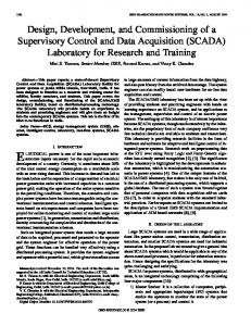
1.2 Geometry and mechanical structure At normal incidence, the prototype has a total depth of 24 radiation lengths, achieved using 10 layers of 0.4 X0 (1.4 mm) thick tungsten absorber plates, followed by 10 layers of 0.8 X0 (2.8 mm) thick plates, and another 10 layers of 1.2 X0 (4.2 mm) thick plates, with an overall thickness of 20 cm. Each silicon layer has an active area of 18 × 18 cm2 , segmented into modules of 6 × 6 readout pads of 1 × 1 cm2 each. The active volume of the physics prototype therefore consists of 30 layers of 3 × 3 modules, giving in total 9720 channels. The design and construction of the prototype presents a number of engineering challenges. A particular innovative effort has been made to minimise passive material zones and to keep the calorimeter as compact as possible, by incorporating half of the tungsten into alveolar composite structures. Three independent structures can be distinguished, as shown in Figure 1, one for each thickness of tungsten. Each structure is fabricated by moulding preimpregnated carbon fibre (Cfi) and epoxy (“prepreg”) onto tungsten sheets, leaving free spaces between two layers to insert the detection units, called detector slabs.
Figure 2. Schematic diagram showing the components of a detector slab.
Figure 1. Schematic 3D view of the physics prototype.
One detector slab, shown in Figure 2, consists of two active readout layers mounted on each side of an H-shaped supporting structure. The slab is shielded on both sides from the tungsten alveolar structure by an aluminium foil 0.1 mm thick, to protect the silicon modules from electromagnetic noise and provide the wafer substrate ground. The H-shaped structure is 326 mm long and 125.6 mm wide, and has a mass of either 1.1, 2.2 or 3.3 kg depending on the tungsten thickness. The active layer is made of a 14-layer printed circuit board (PCB), 2.1 mm thick and 600 mm long, holding high resistivity silicon wafers 525 µ m thick (see Section 1.3). The wafers are cut into square modules of 62 × 62 mm2 , separated from each other by a 0.15 mm wide mounting gap. Two detector slabs are inserted per layer, into the central and bottom cells of the alveolar structure (see Figure 1). The central and bottom slab active areas are formed by an array of 3 × 2 modules and a row of 3 modules respectively. To reduce overlapping passive areas, the two
–3–
Figure 3. Details of the passive areas and layer offsets. Offsets are indicated by single-headed arrows. All distances are in mm.
detection layers of each slab are offset by 2.5 mm in the X direction, as shown in Figure 2. Furthermore, the slabs in each substructure are offset by 1.3 mm in the X direction, as shown in Figure 3. The passive area between modules is mainly due to two 1 mm wide guard rings around the modules (see Section 1.3). A larger passive area is located between the central and bottom slabs, and includes the two guard rings, two 0.15 mm wide mounting gaps between module and PCB, two 0.3 mm thick H structures, two 0.1 mm thick aluminium shields, a 0.3 mm wide global mounting gap,
and a 0.4 mm thick composite sheet, giving a total of 3.8 mm. 1.2.1 Fabrication processes All the composite parts, i.e. H-shaped and alveolar structures, are made using 0.15 mm thick carbon R fibre and epoxy prepreg, TEXIPREG CC120 ET443 [8], with an average thickness of 0.15 mm. Each alveolar structure is made in a single curing step of four hours at 135◦ C. Fifteen metal cores are used to form the alveoli. They are wrapped with one layer of composite, and alternated with tungsten layers to obtain the final structure. Since the thermal expansion coefficient of carbon fibre is very close to that of tungsten, distortions during the curing are small. After curing, the metal cores are taken out, leaving empty spaces for the detector slabs (see Figure 4).
Figure 4. Moulding of an alveolar structure: metal cores alternate with tungsten, both wrapped in carbon fibre-epoxy composite.
Figure 5. Gluing the modules; the accurate positioning of the modules is ensured by a grid of tungsten wires.
–4–
The thin composite sheets located between two cells consist of three composite layers of thickness 0.4 mm. Dimension and geometry tolerances of the structure are directly dependent on the machining of the mould: all pieces were ground with a resulting flatness of ±0.01 mm. Metallic inserts, also included in the composite structure, are used to fasten each structure on its support table. The mechanical and electrical connection of the silicon pads to the PCB is made using EPOR TEK 4110 conductive glue [9]. For the central (bottom) slabs, 216 (108) spots of conducting glue are deposited on each PCB by a pneumatically driven syringe dispenser, mounted on an X-Y automatic robot. The low viscosity nature of the gluing paste keeps the spots correctly shaped during the process. The pressure and the deposit time were chosen to obtain a final spot size between 3 and 4 mm in diameter. The thickness of the glue is calibrated by using nylon spacers 0.12 mm thick. Then, the six (three) modules for the central (bottom) slabs are put on the PCB by hand, as shown in Figure 5. The accurate positioning of each module is ensured during the polymerisation cycle by a grid of tungsten wires, holding the wafers in place. The expected accuracy is ±0.05 mm, arising from the average module size of 61.95 mm and the 62.05 mm imposed by the grid of wires. The curing process is fundamental to the performance of the connection. Curing parameters were chosen to have a good compromise between the final resistance of the connection (< 0.1 Ω) and the mechanical stress applied on the spots of glue. The latter is due to the differential thermal expansion between the PCB and the silicon. The polymerisation of the glue was therefore done at 40◦ C for twelve hours. 1.2.2 Beam test configurations To test the physics behaviour of the ECAL prototype with different impact angles of the beam, a rotational support was designed with six discrete angular configurations, from 0◦ to 45◦ . The position of the three independent alveolar structures can be adjusted according to the chosen angle, to ensure the primary particle will travel through the centre of the active area, as shown in Figure 6. Each structure is mounted on rails, positioned manually and fixed using mechanical pins, with a precision of 0.5 mm, giving an error of ±0.035◦ on the angle. The main error on the angle arises from the manual placement of the ECAL compared to the beam, and is ±0.6◦ .
Figure 6. Example of a rotated configuration at the 45◦ angle setting: schematic 3D view (left) and picture (right) of the prototype at DESY in 2006 (note the staggered slabs and structures).
–5–
In order to vary the impact position of the primary particle on the detector surface, the mechanical support of the prototype has been equipped with a control system allowing for a motion along both the X (±150 mm) and Y (±100 mm) axes, with a precision of ±0.1 mm. The position can be piloted remotely during beam operation. 1.3 Description of the sensitive area The sensors are made from four inch diameter silicon wafers. A resistivity greater than 5 kΩ· cm is necessary to ensure a full depletion with a reasonable bias voltage, and to obtain low bulk leakage currents. A wafer thickness of 525 µ m was chosen, to obtain a signal-to-noise ratio of about 10 at the end of the whole readout electronics chain. The noise of the readout electronics results from the capacitance of the pad itself, the capacitance of the line on the PCB, and the preamplifier noise. A minimum ionising particle (MIP) produces about 80 electronhole pairs per µ m of silicon, hence 42,000 electrons are obtained for the 525 µ m thickness, giving an allowable noise range for the readout electronics of up to 4000 electrons. The crystallographic orientation of the silicon (h111i) has only little importance; the detection of EM showers instead of single particles ensures that the fraction of energy lost through “channeling effects” is very small compared to the total signal. Each wafer is used to make a module, consisting of a matrix of 6 × 6 PIN diodes (pads) of 1 cm2 , as shown in Figure 7. Figure 7. Details of the matrix dimensions in a modThe overall dimensions take into account the ule (cathode side). The area shaded in grey correguard rings. The anode side (N) is common sponds to the guard ring. to all pads. The PIN structure is made with ionic implantation. In order to keep the price and the rate of rejected processed modules low, the manufacturing must be as simple as possible, with a minimum number of steps during processing. The final detector will need about 3000 m2 of such detectors. The passivation layer of the processed module must be compatible with the gluing process described in Section 1.2.1. The main characteristics of a module are presented in Table 1. Wafer diameter Wafer resistivity Wafer thickness MIP deposit Average tile side
4 inch 5 kΩ· cm 525 ± 16 µ m 42 000 electrons 61.95 ± 0.05 mm
Capacitance per pad Full depletion bias voltage Nominal operating bias voltage Break down voltage Leakage current at 200 V
Table 1. Characteristics of a module.
–6–
21 pF 150 V 200 V > 400 V < 350 nA (full matrix)
1.3.1 Module test setup and results
80 70
Leakage current (nA)
Leakage current (nA)
Silicon PIN diode matrices are a priori very simple detectors. Having a whole ECAL covered with high resistivity silicon is however challenging, and implies the necessity to control the process at the earliest stage, in particular in terms of passivation. Therefore several manufacturers were used, enabling testing and validation of several technologies necessary to optimise the production in the future, and minimizing the cost. For the physics prototype, 270 modules are needed. The production of the modules extended from January 2003 to June 2007. All modules are made of raw wafers produced by Wacker [10]. The modules were produced by two manufacturers: the Institute of Nuclear Physics, Moscow State University [11], and ON Semiconductor Czech Republic [12] in conjunction with the Institute of Physics, Academy of Sciences of the Czech Republic, Prague. The two manufacturers use the same basic technique of ion implantation. Guard rings 1 mm thick have been designed around the matrices to reduce surface leakage currents, with two different geometries. For both, the edge termination is made using the floating guard rings technique [13] which does not require any extra step in the fabrication process of modules, helping to reduce the overall cost. Before gluing, the modules are characterised one-by-one by measuring the leakage current as a function of bias voltage (I-V curve), the full depletion voltage (C-V curve) and the stability in time (leakage current versus time at nominal bias). If measurements are taken with a single biased pad, the values are found not to be representative of the performance of the module, especially in terms of breakdown voltage. All 36 pads are therefore biased, using a box specifically designed with 36 contacts made to the module using pin sensors mounted on springs, so as not to damage the surface. Two representative I-V curves taken with this setup are shown in Figure 8.
Maximum depletion voltage
60 50 40
Minimum breakdown voltage
30 20
5000 4000 3000 2000
Operating voltage
Minimum breakdown voltage
Maximum depletion voltage
Operating voltage
1000
10 00
200
400
600
800 1000 Bias voltage (V)
00
50 100 150 200 250 300 350 400 Bias voltage (V)
Figure 8. Leakage current versus bias voltage. On the left is a good module, while on the right the breakdown voltage is too low.
The test bench was used to characterise 550 modules, with an overall yield of 54 %. Wafers were rejected if the full depletion voltage was greater than 150 V, or if the breakdown voltage was less than 400 V, or if the sum of the leakage currents of all 36 pads at the nominal operation voltage of 200 V was greater than 350 nA.
–7–
1.3.2 Calibration of the slabs
Nentries/4 ADC counts
Once validated, the modules were assembled by gluing onto PCBs. Before assembling into a slab, the PCBs were tested in pairs using a cosmic-ray muon test bench, with a dedicated DAQ system. The gluing of each pad and the proper contact with the aluminum foil were checked and a first calibration of each half module, associated with a common readout chip (see Section 2.1), was possible. Initial MIP calibration results for each half module are obtained with a precision of approximately 5 %. An example is shown in Figure 9.
300 mG = -1.3 ± 0.3 ADC counts 250
σG = 8.8 ± 0.3 ADC counts
200
MPV LL⊗ G = 77.1 ± 0.4 ADC counts
150
σLL ⊗ G = 6.2 ± 0.3 ADC counts
100
σG L ⊗ G = 9.0 ± 0.5 ADC counts
50 0 -50
0
50
100
150
200
250 300 Amplitude (ADC counts)
Figure 9. Example of the cosmic-ray muon calibration of a half module showing the signal recorded by the corresponding readout chip. The first peak, centred on zero, is due to the electronics noise (pedestal) and is fitted with a Gaussian function of mean value mG and width σG . The second peak, centred on 82 ADC counts, corresponds to the MIP signal, and is fitted with a Landau (maximum probable value L L ) convolved with a Gaussian distribution of width σ G . The overall fit function is MPVL⊗G and width σL⊗G L⊗G L , σ L ) ⊗ Gauss(σ G ). defined as Gauss(mG , σG ) + Landau(MPVL⊗G L⊗G L⊗G
On average, the signal-to-noise ratio is measured to be 9.1 ± 0.2, with a standard deviation of 1.0 ± 0.1, and less than 0.1 % of the channels are identified as being dead. The quality of the points of glue can be estimated from the noise, since the measured noise increases with the resistivity of the contact point. The chemical passivation of some modules was found not to withstand the gluing process; it was found that the leakage current became greater than 10 µ A per module. This problem has now been solved by the producer. The first slab was assembled in September 2004. Since that time, there has been no evidence of a degradation of the noise due to the gluing process.
2. Electronics and data acquisition The very-front-end (VFE) ASICs used to read out the silicon modules have been specifically designed for the prototype and are called FLC_PHY3. The outputs of the VFE ASICs are transmitted to the off-detector electronics using differential analogue lines. The analogue-to-digital conversion is done on off-detector VME boards, using 16-bits ADCs. Each VME board can read out 96 VFE
–8–
ASICs, and store the digitised data in memory for subsequent readout by an online software system written in C++. 2.1 On-detector readout electronics 2.1.1 FLC_PHY3 ASIC The FLC_PHY3 VFE chip is an 18 channel, charge sensitive, front end circuit. It provides a shaped signal proportional to the input charge. Two chips are hence necessary to read out one module. Having two chips per module also introduces a redundancy into the system by decorrelating ASIC and module behaviour. Each channel is made of a variable gain charge preamplifier followed by two parallel shaping filters of different gain (1 and 10) using a CR-RC shaper, as shown in Figure 10. Each of these shapers is followed by a sample & hold device (referred to as “T&Hold” in Figure 10) driving a single multiplexed output. The bias of each stage is common to all channels. The forward path of the preamplifier consists of an input PMOS transistor used in a common source configuration, ensuring a high transconductance. It is followed by a folded cascade bipolar NPN component. The last stage is made of a PMOS follower. The feedback is made with a switchable capacitance allowing a total feedback from 0.2 pF to 3 pF in steps of 0.2 pF. The DC resistive feedback is ensured by a series of unbalanced current mirrors faking a 22.5 MΩ resistor. This keeps the parallel noise negligible at the working frequency. The shaper is made of a differential input and a single ended output amplifier with an open loop gain of around 100. The filter is a first order active pass-band with a frequency centred at around 1 MHz and a peaking time of 200 ns. This value has been choFigure 10. General block schematic of FLC_PHY3. sen as a trade-off between the serial noise of the preamplifier which performs the optimal shaping around 1 µ s, the trigger latency which forbids a peaking time faster than 150 ns, and the counting rates imposed by the ILC beam structure which require a recovery time below 300 ns to avoid dead time on a pad. The sample & hold is ensured by a 2 pF capacitance followed by a buffer using a Widlar structure. The preamplifier gain is obtained with a nominal feedback capacitance of 1.6 pF allowing a maximum input signal of around 4 pC, equivalent to 600 MIPs. A non-linearity of below 0.3 % up to 500 MIPs is achieved, as shown in Figure 11, and summarised in Table 2. The residuals for the obvious non-linear regions above 3.27 pC (0.3 pC) for gain 1 (10) are not shown. In Monte Carlo
–9–
(MC) simulation and beam test data of a 45 GeV shower, the observed rate of hits recording more than 500 MIPs is about one hit per 500 events. In 100 GeV shower however, the MC simulation predicts about 3.3 hits per event with energy deposit greater than 500 MIPs. This issue will be addressed in the next version of the chip [14].
Figure 11. Output voltage Vout of one channel of the FLC_PHY3 chip as a function of the charge injected Qinj fitted by a linear function (left), and residuals to the fit (right), for gain 1 (top) and gain 10 (bottom), for a feedback capacitance of 1.6 pF.
Shaper gain Qinj max Vout max Preamplifier Gain Measured Feedback capacitance Non-linearity
1 3.27 pC 1.27 V (over 50 Ω) 391 mV· pC−1 1.27 pF 0.32 %
10 0.33 pC 1.12 V (over 50 Ω) 3.44 V· pC−1 1.45 pF 0.36 %
Table 2. Characterisation for a nominal feedback capacitance of 1.6 pF.
The equivalent charge for the noise has been measured on the VFE chip at around 4000 electrons, i.e. 0.1 MIP, with an input capacitance of 80 pF. This capacitance is made up of the detector capacitance of 20 pF added to the PCB line capacitance of 60 pF. The dynamic range hence goes from 0.1 MIP to 600 MIP, thus 13 bits using one shaper gain. The use of the two gains on the shaper in principle increases the dynamic range to 15 bits, although the high gain option was not used for the studies presented here.
– 10 –
From charge-injection measurements, the electronics crosstalk between adjacent channels is found to be less than 0.1 %. 2.1.2 Power consumption The consumption of the whole chip is 150 mW corresponding to 8.3 mW dissipation per channel. It would be easy to reduce that consumption by reducing the input transistor bias current, depending on the noise yield and the input capacitance. Setting a 200 µ A input current makes the consumption fall to 4 mW per channel. 2.1.3 Very Front End boards The 216 channels on the six modules of a PCB from a central slab (see Section 1.2) are read out by twelve FLC_PHY3 chips. Two 16-bit calibration ASICs, each having six channels, are also mounted on the PCB. The VFE ASICs are read out in parallel by the off-detector electronics using twelve differential analogue lines. To reduce the crosstalk below 0.1 %, the lines carrying the signals from the modules are spread on six different planes separated by ground planes, giving the 14-layer PCBs. Depending on the type of slabs on which they will be mounted (i.e. central or bottom row), three variants of the PCBs have been assembled: fully equipped with an array of 3 × 2 modules (30 used and 12 spares), as shown in Figure 12; and left or right equipped (compared to the orientation in Figure 12) with a row of three modules (15 used and 6 spares for each orientation). Figure 12. Picture of the very front end PCB, and A SCSI connector provides the interface description of its elements. PCB thickness: 2.1 mm, to the off-detector electronics, allowing a full length: 600 mm, largest width: 12.4 mm. differential link in order to dissociate the digital ground in the readout crate from the detector ground. Each VFE ASIC has a separate channel to the connectors, i.e. there is no further multiplexing on the VFE board. The data transmission is analogue and the analogue-to-digital conversion is done on the off-detector board. A differential buffer is used to convert the single-ended signal provided by the VFE ASIC before transmission. A reference is used for each chip. The digital links are RS-422, allowing a wide common mode range to correct the voltage shift between the VFE PCB, supplied with a negative voltage to optimise the noise, and the off-detector board, supplied with a positive voltage. 2.2 Off-detector electronics The basic requirements of the off-detector electronics are: to distribute the sample & hold signal
– 11 –
required by the VFE electronics within a latency of 180 ns and with an uncertainty of less than 10 ns; to provide the digital sequencing necessary to multiplex the analogue signals from the VFE PCBs; to digitise the signals; and to store the data. The analogue signals have a 13-bit dynamic range, and the electronics is required not to contribute significantly to the analogue noise. Assuming a standard beam test spill structure, the target for the electronics is to run at an event rate of 1 kHz during the beam spill, with an overall average rate of 100 Hz. 2.2.1 Implementation The calorimeter readout is based on the “Calice Readout Cards” (CRC) [15]. These are customdesigned, 9U, VME boards derived from the Compact Muon Solenoid tracker Front End Driver readout boards [16] but with major modifications to the readout and digitisation sections. Each CRC consists of eight front-end (FE) sections feeding into a single back-end (BE) which provides the interface to VME. The whole board is clocked from an on-board 40 MHz oscillator. Each FE section can control one full or two half VFE PCBs, totalling 12 VFE readout ASICs, each with 18 multiplexed channels, and hence a total of 216 channels. The FE section consists of a pair of 68-pin mini-SCSI connectors, twelve 16-bit ADCs (one for each readout ASIC) and a Xilinx Virtex-II FPGA. Mini-SCSI cables of 10 m length are used to connect the FEs directly to the VFE PCBs. The digital signals on the mini-SCSI connector are all LVDS and are tracked directly to the FPGA. All VFE ASIC control and clocking signals are generated in the FE FPGA, including the time-critical sample & hold signal edge. The FPGA derives a 160 MHz clock from the 40 MHz board clock, allowing signal timing to 6.25 ns. The FE section also contains two 16-bit DACs for calibration purposes. These can be internally fed back into the ADCs directly, or can be sent onto the mini-SCSI connector to allow calibration of the VFE ASIC. The total data volume within each FE per event for 18 multiplex samples is 512 bytes, including an eight-byte header. The BE section consists of a Xilinx Virtex-II FPGA controlling an 8 MByte memory. It distributes configuration data to each FE section and gathers the digitised event data from each before storing it in the memory for subsequent readout. Each CRC is capable of reading out 1728 channels. The data volume per event from these channels is 4 kBytes, allowing 2000 events to be stored in the memory before readout is required. Six CRCs are required for the full ECAL readout of 9720 channels and these are housed in a single VME crate. The VME interface used is the SBS620 VMEbus-PCI bridge [17]. Some systems other than the CRC VME readout are also integrated into the online system. Tracking (see Section 3) is done using commercial VME TDC units which are installed in spare slots of the CRC crates. Slow data control and readout is implemented via sockets to independent slow control systems. All slow data are written into the data files to ensure the raw data are selfcontained. 2.2.2 Trigger and timing A specific VME slot near the centre of the crate is chosen as the trigger control and distribution CRC and a custom backplane is used to take triggers from this central location to the other CRCs in the crate. The backplane is a simple point-to-point PCB, press-fit to the J0 connectors. The trigger distribution and control is generated in the BE FPGA of the trigger slot CRC and fanned out to the
– 12 –
other CRCs. A second fanout on the CRC allows a duplicate set of trigger signals to be taken via a cable to an identical backplane in a second crate, for readout of more than one calorimeter. The trigger input signals are LVDS and are fed into the J2 connector. The trigger logic is performed within the BE FPGA, allowing significant complexity in the trigger condition to be set via software. This also controls the trigger busy signal, preventing further triggers until the digitisation of the VFE analogue data has been completed. The trigger rising edge provides the system synchronisation signal and all timings, including those for the time-critical sample & hold, are derived from this edge. To ensure complete events can be built from the same trigger, independent trigger counters are implemented in each of the FE and BE FPGAs, and are read periodically, both during and at the end of each beam spill. If any discrepancy between the counters is observed, all data from the spill following the last valid counter readout are discarded offline. All trigger inputs, as well as several other input signals, are recorded in a trigger history buffer. This consists of 32 bits, one for each signal, sampled on the 40 MHz clock, recording their state for 256 samples around the trigger time. This allows the detailed time structure of the trigger logic to be observed as well as the readout of several other beam line elements such as veto scintillator ˇ counters and a Cerenkov detector. 2.2.3 Performance The complete system performed well in the beam test environment. The sample & hold is distributed on the derived 160 MHz clock within a minimum of 160 ns, allowing the rest of the latency of 180 ns to be implemented as a software-specifiable delay in the FE FPGA. The jitter on this is dominated by rounding to the 6.25 ns clock period. The 16-bit ADCs allow both positive and negative signals although only the upper half is used for the ECAL readout. This still allows them to meet the 13-bit dynamic range requirement, with the two extra bits covering any differential non-linearities or other biases in the ADCs. The CRC noise when the ECAL is disconnected is very low, with an average of 1.4 ADC counts, compared to around 5.9 ADC counts from the ECAL VFE electronics (see Section 4.2.2). The trigger counter synchronisation is very reliable, with a rate of less than one trigger missed on any CRC per million events, resulting in an average event loss of less than one per thousand. Two significant problems were identified. Firstly, insertion and removal of the cables from the mini-SCSI connectors resulted in breaks in the solder joints, in nearby traces, and in solder connections to nearby FE components, most of which have been fixed by hand. Secondly, there were also problems with the reliability of some of the PCB layer interconnects, and several wires have been added to bypass vias which developed high resistivity. Overall, the system had errors on 3 out of 112 FE sections, none of which were used for data taking. 2.2.4 Readout software The online software must support the electronics requirements of 1 kHz instantaneous and 100 Hz average event rates. The maximum event size to be handled is 64 kBytes, allowing for readout of two calorimeters and other beam line equipment. The system is also required to be flexible, so as to handle different beam lines and spill structures.
– 13 –
The code is written in C++ and is specific to Linux, being POSIX compliant as much as possible. No database is used in the online system; all configuration of the hardware is stored in the run data files so that any run can be fully characterised from the data file itself. The full system achieves a readout rate of 120 Hz when not limited by the beam intensity or spill structure. The average rate during higher intensity spills is found to be around 90 Hz. The trigger rate during spills does not reach 1 kHz but is limited to around 600 Hz. This is mainly determined by the fraction of events for which the trigger counters are read out. These are read with a high frequency to be conservative in checking for synchronisation errors; a lower fraction would allow the specified trigger rate of 1 kHz to be achieved. The system has recorded up to 10 million events per day and has run efficiently for several beam periods totalling nearly three months. Including 2007 data, around 300 million beam events have been taken, amounting to around 30 TBytes of data.
3. Beam tests Large scale beam tests are conducted in order to demonstrate the principle of a highly granular Si-W electromagnetic calorimeter. Data analyses are ongoing which will quantify the energy and spatial resolutions, and validate the existing models of electromagnetic and hadronic showers, e.g. the various GEANT4 [18] models. The studies in this article focus on the basic hardware performance when the device is exposed to high energy particles. 3.1 Beam lines at DESY and CERN in 2006 In May 2006, the ECAL prototype was tested with electron beams at DESY, equipped only with 24 layers of central slabs (see Section 1.2). A sketch of the beam test setup is shown in Figure 13. The beam trigger is defined by the coincidence signal of two of the three scintillator counters, referred to as Sc1, Sc2 and Sc3 in Figure 13. The size of the beam can also be defined by two scintillator counters, mounted in a cross shape (Fc1 and Fc2 in Figure 13). Four drift chambers (DC1, DC2, DC3 and DC4) are used to monitor the beam and reconstruct tracks. All distances are in mm 8
8 100
300
100 5
4520
520
420
900
8
5 10
650
370
2
342
600
Fc2
Collimator Sc1
FRONT
100
100
10 10
DC4
DC3
Fc1
DC1
DC2 Fc2
Sc1 and Sc2 are 200x200 Sc3 is 120x120
5
50
Sc2
Sc3
ECAL
z=0
45 Fc1
70 5
Figure 13. Sketch of the DESY beam test setup in May 2006. All distances and components dimensions are in mm, along the beam axis. The beam enters from the left side. See text for explanations of the components.
– 14 –
In August and October 2006, the ECAL was tested at the H6 area at CERN, in combination with an analogue HCAL prototype [19] and a Tail Catcher and Muon Tracker prototype [20], using electron and pion beams. The 30 layers of the ECAL prototype were equipped with central slabs. Sketches of the beam line for both periods are presented in Figure 14. In August, the distance between ECAL and HCAL was large enough to allow the ECAL to be rotated. In October however, the accent was put on minimising this distance so as to use the ECAL as a tracker for pion events. The beam trigger is defined by the coincidence signal of two of the three scintillator counters (Sc2, Sc3 and Sc4 in the August setup, Sc1, Sc3 and Sc4 in the October setup). When it was not used in the trigger, the largest scintillator (Sc3 in August, Sc4 in October) was still read out and so could be used as a beam halo veto offline, using a lack of coincidence between the 10 × 10 and 20 × 20 cm2 scintillators. Three delay wire chambers [21] (DC1, DC2, DC3 in Figure 14) are used to monitor ˇ the beam and reconstruct tracks. A Cerenkov detector is used to separate electrons from pions. Muons are identified by two scintillators (Mc1, Mc2) placed behind the HCAL prototype. 15 11000
58 15 25000
1760
548 Sc1
22
118
Sc2
DC3 Cerenkov
58 26 DC1
726
655
60
584
60
Sc4 ECAL
Sc3
9.5
1458
8
460
DC2
Sc1 is 30x30 Sc2 and Sc4 are 100x100 Sc3 is 200x200
9.5
1136
201
58
8
HCAL
Mc1
TCatcher
Mc2
1458
9.5
z=0
DC1,2,3
All distances are in mm
Mc1 and Mc2 are 1000x1000
100
FRONT 100
15 11000
58
8
201
58
58
969
8 15
25000 Cerenkov
32 Sc1
118
1790 DC3
34
Sc4
1427 Sc3
DC1
DC2
Sc2 is 30x30 Sc1 and Sc3 are 100x100 Sc4 is 200x200
460
571
57
ECAL
z=0
127
52
Sc2 HCAL
TCatcher
Mc1
Figure 14. Sketch of the CERN beam test setups in August (top) and October (bottom) 2006. All distances and components dimensions are in mm, along the beam axis. The beam enters from the left side.
3.2 Summary of the data collected Various scans were performed in order to characterise the prototype. The energy of the electron beams was varied from 1 to 6 GeV at DESY, and from 6 to 50 GeV at CERN, to study linearity and resolution. The beam was positioned near the centre, edge and corner of the wafers to study the uniformity of the wafers and the impact of the passive areas. Events with positrons were also taken from 6 to 50 GeV. The ECAL prototype was rotated by 10◦ , 20◦ , 30◦ and 45◦ with respect to the beam direction to study the effects of angular incidence on the linearity and resolution. Finally, π + and π − beams were taken with energies from 6 to 80 GeV.
– 15 –
Over 22 million events were collected with electron beams, as detailed in Table 3, and 25 million events with pion beams. In addition, more than 57 million muon events were collected for calibration purposes (see Section 5). An event display of an electron event at 30 GeV is shown in Figure 15. Location Angles Particle
0◦
1 GeV 1.5 GeV 2 GeV 3 GeV 4 GeV 5 GeV 6 GeV Total
400 486 400 304 400 304 594 2888
10 ◦
DESY (kEvt) 20 ◦ 30 ◦ e−
300 200 200 200 224 300 688 2112
345 200 200 200 200 200 200 1545
200 300 300 324 300 325 185 1934
45 ◦ 200 200 200 200 200 200 200 1400
Location Angles Particle 6 GeV 8 GeV 10 GeV 12 GeV 15 GeV 16 GeV 18 GeV 20 GeV 30 GeV 40 GeV 45 GeV 50 GeV total
0◦ e+ 208 152 476 310 303 390 409
305 2553
CERN (kEvt) 20 ◦ 30 ◦ e− e−
45 ◦
128 218 469 211 325
594
530
181
244
250
330 550 280 753
208 531 311 551
742
2688
2375
231 590 685 347 933 4137
112
110 270
Table 3. Summary of the 22.4 million triggers collected at DESY and CERN with electron beams.
Figure 15. Event display showing a 30 GeV electron showering in the ECAL, in a run taken at CERN in August 2006. Only hits with an energy above 0.5 MIP are displayed. The colour scale represents the energy deposited per pad, in units of MIP. Top-left: X −Y projection, top-right: Y − Z projection, bottom-left: X − Z projection.
– 16 –
4. Pedestal, noise, and crosstalk around module edge A data-taking run consists of 500 pedestal events, 500 events with charge injection via the calibration chips, and between 10,000 and 40,000 beam data events, after which the sequence repeats. The pedestal and calibration events are taken with a random trigger occurring outside the beam spill period. In addition, pedestal events are taken during the beam spill (every 25 beam events on average), to check the influence of the beam on the pedestals. The determination of the pedestals and noise for the individual channels is described in the following sections. In these sections, the conversion from ADC counts to MIP equivalent units uses the factor 46 ADC counts per MIP (see Section 5). 4.1 Pedestal subtraction procedure For a given channel, the pedestal is defined by the mean value of the signal recorded with no beam, i.e. coming from electronics, and the noise by the corresponding standard deviation. Instabilities occurring in the time between two sets of pedestal events need to be considered and accounted for in the pedestal subtraction procedure described here. Correlations in the noise also need to be checked, and accounted for if induced by pedestal drifts, and will be described in Section 4.1.2. Once the pedestal subtraction procedure is trusted, the uniformity, the stability in time of any remaining offsets, and the noise in beam-induced events all need to be measured. The results are presented in Section 4.2. 4.1.1 VFE PCB-wise correlated pedestal shifts The pedestals of all the channels of one VFE PCB are shown, as a function of time, in Figure 16. In this figure, a clear shift in the raw ADC values can be seen between two sets of pedestal events (identified by the blank columns at 680 s and 1030 s). This unexpected effect of pedestal shifts of up to 100 ADC counts (equivalent to approximately two MIPS) for all the channels of a VFE PCB is observed frequently in beam data events. The origin of these shifts has been traced to the non-isolation of the VFE PCB power supply lines, which results in changes to the working point of the output signal lines. This will be corrected in the next PCB design. In a first iteration, pedestal and noise values are obtained by calculating the mean and standard deviation of the ADC count distribution per channel in the 500 pedestal events taken at the start of each sequence. Averages calculated from a set of pedestal events are then simply subtracted from the ADC values recorded in the following set of beam events. The shift in the pedestals will affect the apparent noise, as the reference value is fixed by the previous set of pedestal events: the noise will appear to be artificially large, and 100 % correlated within the PCB if the shift is common to all channels. The left-hand plot of Figure 17 shows the correlation coefficients (averaged over one run) between the apparent noise on the 216 channels of a particular VFE PCB, calculated after this simple pedestal subtraction. Channels are ordered by wafers, so 36 consecutive channels belong to the same wafer in the readout channel index displayed. The apparent noise is highly correlated between all channels, indicative of a common shift in the pedestal values. It is therefore important to correct the pedestals on an event-by-event basis, by detecting and correcting shifts compared with the previous estimate. Hence, a second iteration on the pedestal value is performed. A sample of channels is defined on each VFE PCB by selecting modules
– 17 –
ADC value (ADC counts)
400
200
0
-200
-400
-600 0
200
400
600
800
1000 1200 Elapsed time (s)
1 200
0.8
180
0.6
160
0.4
140 0.2 120 -0
100
Readout channel index
Readout channel index
Figure 16. ADC values recorded in all 216 channels (each set of points represents one channel) of the VFE PCB situated in the 24th layer, as a function of time (seconds since the beginning of the run), in beam events in a muon run taken at CERN in August 2006.
1 200
0.6
160
0.4
140 0.2 120 -0
100
-0.2
80
0.8
180
-0.2
80
60
-0.4
60
-0.4
40
-0.6
40
-0.6
20
-0.8
20
-0.8
0 0
20
40
60
80
100
120
140
160
180
200
-1
Readout channel index
0 0
20
40
60
80
100
120
140
160
180
200
-1
Readout channel index
Figure 17. Noise correlation coefficient (colour scale) between all pairs of channels for the VFE PCB situated in the third layer, in a 45 GeV electron run taken at CERN in August 2006, after the simple pedestal subtraction. Left: before correcting the pedestal shifts, the mean correlation is 0.4207 ± 0.0004 with a standard deviation of 0.0551 ± 0.0002. Right: after corrections, the mean correlation is −0.0017 ± 0.0003 with a standard deviation of 0.0519 ± 0.0002.
without signal hits. For this purpose, it is assumed that a signal was recorded if the difference between the minimum and the maximum of the pedestal-subtracted ADC values of the 36 channels in a module exceeds 3000 ADC counts. For this sample, a first estimate of the mean pedestal value is taken to be the average of the minimum channel value per chip, plus five times the noise. The root-mean-square (RMS) deviation from this mean is calculated using only the channels having ADC values smaller than the mean. This is to avoid being biased by the signal. For each VFE PCB, a single offset is then estimated by iterating on the mean value (and hence the channels taken into account in the calculation of the RMS) until the RMS is compatible with the mean noise of the PCB, with a maximum of 20 iterations. The right-hand plot of Figure 17 shows the noise correlation
– 18 –
coefficients after applying this procedure. The mean correlation is reduced to −0.0017 ± 0.0003, indicating that the procedure has successfully corrected for the shifts. 4.1.2 Correlated noise and signal-induced pedestal shift
1 200
0.8
180
0.6
160
0.4
140 0.2 120 -0
100
Readout channel index
Readout channel index
Some modules recording a high signal are subject to a different effect, namely a signal-induced pedestal shift (SIPS), resulting in apparent high noise correlations for all 36 channels on a module. This can be seen in Figure 18, left, for the VFE PCB situated in the tenth layer, for the same run as in Figure 17, after applying the corrections described in Section 4.1.1. 1 200
0.6
160
0.4
140 0.2 120 -0
100
-0.2
80
0.8
180
-0.2
80
60
-0.4
60
-0.4
40
-0.6
40
-0.6
20
-0.8
20
-0.8
0 0
20
40
60
80
100
120
140
160
180
200
-1
Readout channel index
0 0
20
40
60
80
100
120
140
160
180
200
-1
Readout channel index
Figure 18. Noise correlation coefficient (colour scale) between two channels for the VFE PCB of the tenth layer, in a 45 GeV electron run taken at CERN in August 2006. Left: before SIPS corrections, the mean correlation is 0.019 ± 0.001 with a standard deviation of 0.156 ± 0.001. Right: after SIPS corrections, the mean correlation is 0.0058 ± 0.0001 with a standard deviation of 0.0194 ± 0.0001.
Pedestal shift (ADC counts)
However, the SIPS effects are not systematic, in that they do not affect all PCBs, and, for those affected, the effect is not always present. What is inducing this phenomenon is not yet understood, but a possible explanation could be that there is an intermittent bad contact between the aluminum foil and the module. A common 0 serial resistance to all pads of a few Ohms would produce the same effect. A strong cor-50 relation between the negative pedestal shift -100 and the amplitude of the signal is observed, as shown in Figure 19. -150 The SIPS are corrected on an event-byevent basis. Inspired by the corrections de-200 0 10000 20000 30000 40000 scribed in Section 4.1.1, averages are conAmplitude (ADC counts) sidered per module, rather than per PCB, Figure 19. Pedestal shift in the top row, middle moddiscarding hits with signal, and iterating on ule of the 11th layer as a function of the signal amplithe mean, standard deviation, and channels tude summed over all 36 channels, in a 45 GeV electaken into account in the calculations. The tron run taken at CERN in August 2006. The average result after corrections can be seen in Figper bin in X is displayed in blue circles. ure 18, right. The corrections perform well, the average correlation over the whole PCB being reduced by a factor of three, and the standard deviation of the correlation coefficients by one order of magnitude.
– 19 –
4.2 Uniformity and stability of the residual pedestals and noise For more systematic studies of uniformity and stability in time and temperature, the residual pedestal and noise will from now on be defined by the mean RG and standard deviation NG of the Gaussian fit of the noise component of the spectrum in beam induced events (see first peak in Figure 9), after pedestal subtraction and all corrections as described above. Noise and residual pedestal values are verified to be stable within a run. The full statistics of each run is hence used to perform the fit, and the run dependence studied. The uncertainties on the residual pedestal RG and noise NG in the following sections arise from the uncertainties from the fit on each parameter. The noise peak is fitted iteratively in the range [RG − 5 NG ; RG + 1 NG ], to avoid being biased by the signal. By varying the fit range, an additional systematic uncertainty of ±0.3% × NG is found and added in quadrature to the uncertainty on the noise. 4.2.1 Uniformity and stability of the residual pedestals
R G (ADC counts)
Figure 20 shows the residual pedestals for a particular run taken with electrons, as a function of the pad index. The pad index is defined as 6 × 36 × K + 36 × (2 × WC + WR − 1) + (6 × PC + PR), where K is the layer index, WR (WC ) is the module row (column) index, and PR (PC ) is the pad row (column) index. Results are not shown for the nine channels (out of 6471 active channels, see Section 5.2) where the Gaussian fit to the noise peak did not converge. The average residual pedestal over all channels is −0.03 ± 0.01 ADC counts for this particular run, with a standard deviation of 1.05 ± 0.01 ADC counts. A larger scattering can be seen around the shower maximum, indicating a possible remaining influence of the SIPS described in Section 4.1.2. A periodic structure may be noted, whose period is 216 channels, i.e. PCB-related, and reflects the differences in length of the electronics connection from each pad to its readout chip. CALICE
4 2 0 -2 -4 -6 0
400 350 300 250 200 150 100 50 0 -3
Entries 6462 Mean -0.025 ± 0.013 RMS 1.051 ± 0.009 1000
2000
-2
-1
0
1
2
3
RG (ADC counts)
3000
4000
5000
6000 Pad index
Figure 20. Uniformity of the residual pedestals RG as a function of the pad index (see text), for a 45 GeV electron run taken at CERN in August 2006. The inset histogram displays the projection on the y-axis.
– 20 –
0.2
CALICE
Pion/muon runs -
0.15
e+/e runs
0.1 0.05 -0 -0.05 -0.1 600
620
640
660
680
RG standard deviation (ADC counts)
R G mean (ADC counts)
Figure 21 shows the mean and standard deviation of the residual pedestals averaged over all channels, for other runs taken in October 2006, as a function of the run number. Very similar results are obtained for the August runs. Pion and muon runs have systematically less spread between channels than electron runs, and a mean value closer to zero, indicating again a possible remaining influence of the SIPS on the pedestals. 1.4
-
e+/e runs
1.2 1 0.8 0.6 0.4 0.2
700 720 740 760 Run number (300XXX)
CALICE
Pion/muon runs
600
620
640
660
680
700 720 740 760 Run number (300XXX)
Figure 21. Time dependence of the average over all channels of the residual pedestal RG : mean value (left) and standard deviation (right) as a function of the run number, for runs taken at CERN in October 2006.
CALICE 350 August 300 250
October Entries 6471 Mean 0.081 ± 0.008 RMS 0.610 ± 0.005
Entries 6471 Mean 0.054 ± 0.010 RMS 0.774 ± 0.007
200
August runs
150
Nentries/0.04 ADC counts
Nentries/0.04 ADC counts
On average over all channels, the pedestals in electron runs are subtracted with a remaining positive offset of 0.080± 0.013 ADC counts (0.20± 0.02 % of a MIP). The residual standard deviation channel-to-channel is however 0.80 ± 0.05 ADC counts (1.9 ± 0.1 % of a MIP), which justifies investigating the channel dependence in the following. The residual pedestal per channel and per run is found to not have any clear dependence on time or temperature, with no observable day/night variations, nor any dependence on the beam energy of the run. In order to study more systematically the time dependence for each channel, the mean and standard deviation over all runs weighted by the error per run are considered per channel, and displayed in Figure 22 for all channels, for CERN electron runs. The mean pedestal offset is smaller than 0.17 ± 0.02 % of a MIP with a standard deviation channel-to-channel of 1.67 ± 0.02 % of a MIP. The residual offset run-to-run is of the order of 1.1 ± 0.1 % of a MIP, with a standard deviation channel-to-channel of 0.48 ± 0.01 % of a MIP.
October runs
800
600 500
0 1 2 3 RG weighted mean (ADC counts)
RMS 0.206 ± 0.002
RMS 0.220 ± 0.002
October runs
100 -1
Entries 6471 Mean 0.473 ± 0.003
August runs
50 -2
Entries 6471 Mean 0.510 ± 0.003
300 200
-3
October
400
100
0 -4
CALICE August
700
0 0
0.2
0.4
0.6 0.8 1 1.2 1.4 1.6 1.8 2 RG weighted standard deviation (ADC counts)
Figure 22. Weighted averages over all runs of the residual pedestal RG per channel: weighted mean (left) and weighted standard deviation (right) for all channels, for electron runs taken at CERN in 2006.
The effect of a systematic pedestal offset on the energy scale is additive, and so the mean
– 21 –
offset scales with the number of hits recorded. To give an estimate of the size of the effect, a 1 GeV (45 GeV) electron will produce around 250 MIPs (6000 MIPs). If these are distributed over 100 (400) hits, the impact of the remaining pedestal offset will be around 0.2 MIP (0.8 MIP), i.e. ≃1 MeV (≃3 MeV), which can be neglected. 4.2.2 Uniformity and stability of the noise
NG (ADC counts)
Figure 23 shows the noise per channel as a function of the same pad index as used in Figure 20, and for the same electron run. Some channels have an intrinsically high noise, often in (anti)correlation with a neighbouring channel. On average over all channels, the noise with this method is found to be 5.914 ± 0.004 ADC counts with a standard deviation of 0.345 ± 0.003 ADC counts, for this particular run.
18
CALICE
400
16
Entries 6462
300
14 12
200
Mean 5.914 ± 0.004
100
RMS 0.345 ± 0.003
0
5
10
6 7 8 NG (ADC counts)
8 6 40
1000
2000
3000
4000
5000
6000 Pad index
Figure 23. Uniformity of the noise NG as a function of the pad index (see text) for a 45 GeV electron run. The inset histogram displays the projection on the y-axis.
Figure 24 shows the mean and standard deviation of the noise averaged over all channels, for other runs taken in October 2006, as a function of the run number. Very similar results are obtained for the August runs. On average over all channels, the noise is 5.962 ± 0.009 ADC counts (12.9 ± 0.1 % of a MIP), with a run-to-run dependence smaller than 1 % of the mean noise, and a channel-to-channel dependence of about 9 % of the mean noise, which justifies considering the channel dependence in the following. As for the residual pedestal, no clear correlations are seen as a function of time, temperature (day/night variations), or beam energy. In order to study more systematically the time dependence for each channel, the mean noise value over all runs weighted by the error per run is considered per channel, and displayed for all channels in Figure 25, left, for CERN electron runs. The mean noise is 12.9 ± 0.1 % of a MIP, with a spread channel-to-channel of 1.1 ± 0.1 % of a MIP. The standard deviation in time is smaller than 0.3 % of a MIP on average, with a spread channel-to-channel of
– 22 –
6.05
CALICE
Pion/muon runs -
e+/e runs
6 5.95 5.9 5.85 5.8 5.75 5.7 600
620
640
660
680
NG standard deviation (ADC counts)
NG mean (ADC counts)
6.1
0.75
CALICE
Pion/muon runs -
e+/e runs 0.7 0.65 0.6 0.55 0.5
700 720 740 760 Run number (300XXX)
600
620
640
660
680
700 720 740 760 Run number (300XXX)
Figure 24. Time dependence of the average over all channels of the noise NG : mean value (left) and standard deviation (right) as a function of the run number, for runs taken at CERN in October 2006.
CALICE August 102
October
Entries 6471
Entries 6471
Mean 5.948 ± 0.006
Mean 5.958 ± 0.006
RMS 0.486 ± 0.004
RMS 0.498 ± 0.004
Nentries/0.4%
Nentries/0.04 ADC counts
less than 0.2 % of a MIP. The standard deviation per channel normalised by the corresponding noise per channel is represented in Figure 25, right. On average over both periods, the relative spread run-to-run is 2.00 ± 0.03 % with a spread between channels of 1.60 ± 0.01 %. With about 20 % of the channels having run-to-run variations above 3 %, a run-by-run approach to measure the noise is required. The impact of the noise on the energy scales with the square root of the number of hits: for 100 (400) hits in the case of a 1 GeV (45 GeV) incident electron, the noise contributes less than √ 0.5 %/ E to the total energy resolution. CALICE August Entries 6471 Mean 2.220 ± 0.020 RMS 1.592 ± 0.014
3
10
102
October Entries 6471 Mean 1.886 ± 0.021 RMS 1.686 ± 0.015
August runs
10
October runs
1 4
August runs 10
October runs
1 6
8
10 12 14 16 NG weighted mean (ADC counts)
0
2
4
6
8
10
12
14
16
18
20 22 24 Resolution (%)
Figure 25. Weighted mean over all runs (left), and resolution, defined as the ratio of the weighted standard deviation to the weighted mean (right), of the noise NG per channel for all channels, for electron runs taken at CERN in 2006.
4.2.3 Conclusion Pedestals are subtracted with a remaining offset smaller than 0.2 % of a MIP, but with channel-tochannel variations of 1.7 ± 0.1 % of a MIP, and run-to-run variations of 1.1 ± 0.4 % of a MIP. The impact on the energy scale depends on the number N of hits recorded, 0.002 × N in MIP units, which can be neglected. The noise per channel is 12.9 ± 0.1 % of a MIP on average for all channels, with variations in time averaged over all channels of 2.00 ± 0.03 %. About 20 % (6 %) of the channels have time variations greater than 3 % (5 %), requiring a run-by-run approach to extract the noise measurements.
– 23 –
√ The impact on the energy resolution also depends on the number N of hits recorded, 0.13 × N in MIP units. Since N ≃ 100 (400) for 1 GeV (45 GeV), this is therefore negligible. 4.3 Crosstalk around the module edge
pad index
In some events (as shown in the event display in Figure 26), when a large quantity of energy is deposited in the proximity of the guard rings, a signal of almost constant amplitude appears on all peripheral pads, except for the four pads of the corners where this amplitude is twice as large. These “square events” are due to capacitive coupling which exists between the guard rings and the peripheral pads. From the measurements, about 1% of the charge deposited in the guard ring is propagated into each border pixel (and twice as much into the corner pixels), which is compatible with the simulation of a simple electrical model shown in Figure 27. 18
102
16 14 12
10
10 8 6
1
4 2 0 0
2
4
6
8 10 12 14 16 18 pad index
Figure 27. Simple electrical model of capacitive coupling of pads to the guard rings.
Figure 26. Example of a square event, taken at CERN with a 45 GeV electron beam at normal incidence, in the 12th layer. The colour scale represents the energy deposited per pad, in units of MIP.
Following the idea of a capacitive coupling between guard rings and bordering pads, a straightforward option is to cut the guard rings into small segments. This layout technique should result in the coupling capacitance being in series, thus dividing the coupling effects. Following preliminary simulation studies, the segmented topology design option for the guard rings is shown to lower the crosstalk effects by a factor ranging from 3 to 30 according to the actual distances of the elements of the design. The simulation work is ongoing and other design options are being evaluated. Measurements on real modules will complete this work. The criterion for identifying square events in the beam test data is based on two characteristics of the border hits involved in square patterns. Firstly, a border hit is considered as isolated if its neighbours are only other border hits. Secondly, two border hits are linked if there is a path between them along the border without any gap. In a module, a square pattern is found each time the number
– 24 –
Rate of modules with square patterns
of border hits which are isolated and linked is greater than nine, established with the help of Monte Carlo data. The Monte Carlo does not include the simulation of the crosstalk. The probability for a module to display a square pattern according to the above criterion is shown in Figure 28 for both August and October periods of data taking at CERN. The error bars displayed in Figure 28 contain the systematic uncertainty associated with varying the selection cut between eight and ten linked border hits, in quadrature with the statistical uncertainty. It is seen that, as expected for a crosstalk effect with a detection threshold, the rate increases with the energy of the electron beam, but remains stable in time for a given energy and beam profile. For both periods, the beam was pointing towards a guard ring, but its geometrical spread was larger in August. This leads to a higher rate of square patterns in October, since the rate also increases when the particle becomes closer to the guard ring. Given this geometrical consideration, it is not reliable to quote a rate of square events independent of a particular beam setting.
10-3
CALICE
10-4
10-5
6 GeV 8 GeV 10 GeV 12 GeV
-6
15 GeV
10
18 GeV 20 GeV 30 GeV 45 GeV
-7
10
10-8
200
300
400
500
600
Run number (300XXX)
Figure 28. Square pattern rate per module for a particular algorithm (see text), for runs taken at CERN in August and October 2006. Energies from 6 to 45 GeV are displayed.
5. Calibration of the detector Muons are used to calibrate the detector in terms of MIPs. After checking the stability in time of the noise component in muon events, the conversion factor from ADC counts to MIP equivalent energies needs to be extracted per channel, using a large sample of muon data to reduce the statistical fluctuations. The uniformity and the stability in time of the calibration constants need to be checked, as well as the possible sources of systematic uncertainties that will influence any energy measurement. The method and results are detailed in the following sections.
– 25 –
5.1 Extraction of the calibration constants per channel The calibration of the ECAL prototype was performed using 74 beam halo muon runs (≃ 250, 000 events each), recorded during October 2006. A further 18 runs were recorded in August 2006. Another experiment upstream helped to provide a wide spread of the muon beam over the whole surface of the prototype. Events were triggered with a 1 m2 scintillator counter. An event display of a muon event is shown in Figure 29.
Figure 29. Event display showing a muon crossing all 30 layers of the ECAL, in a run taken at CERN in October 2006. A threshold of 0.5 MIP has been applied. The colour scale represents the energy deposited per pad, in units of MIP. Top-left: X − Y projection, top-right: Y − Z projection, bottom-left: X − Z projection.
The first stage in the analysis of muon events is substract the pedestals from the raw data, as described in Section 4.1. The pedestal subtraction is performed with an accuracy of 0.1 ADC counts (0.2 % of a MIP) on average for all channels, taken as a systematic uncertainty for the calibration constants. The calibration constants are calculated for each channel using the hit energy distribution in identified beam halo muon events. The event sample is selected by requiring the presence of a track which is consistent with being a MIP, based on two criteria. Firstly, the total number of reconstructed hits in the 30 layers of the ECAL must be between 15 and 40. Secondly, the distance between two hits in consecutive layers must be less than 2 cm. As the residual pedestals are shown to be negligible compared to the estimated MIP signal (0.2 % of a MIP), they are not subtracted from the measured value of the MIP peak position. Furthermore, with a mean noise of 12.9 ± 0.1 % of a MIP, the noise tail is neglected and only the MIP contribution in the hit energy distribution is fitted. For each channel, the distribution of hit energies (in ADC counts) is made from the sample of selected muons. Since the muon spread is not totally uniform over the whole surface, the number
– 26 –
Nentries/2.5 ADC counts
of hits in the distributions varies from a few thousand in the border regions to up to 14,000 in the central part. The hit energy distribution is fitted to a convolution of a Landau distribution and a Gaussian. An example fit is shown in Figure 30. The most probable value GL of the Landau function gives the calibration constant, while the standard deviation of the Gaussian σG gives an estimate of the noise value for each channel. The fitting range has been limited between 25 and 78.5 ADC counts. Normalisation 4075.8 ± 177.7 GL 45.5 ± 0.1 σL 3.1 ± 0.2 σ G 6.6 ± 0.2
1000 800 600 400 200 00
50
100
150 200 250 Hit energy (ADC counts)
Figure 30. A representative example of the energy distribution of hits in muon events for a particular channel. The fit function is a convolution of a Gaussian and a Landau. Normalisation, GL and σL refers to the constant, most probable value and width of the Landau function, and σG to the width of the Gaussian function.
The statistical uncertainty on the fitted value of GL , calculated by TMinuit [22], is 0.243 ± 0.001 ADC counts on average for all channels, with a spread between channels of 0.063 ± 0.001 ADC counts. In addition, as stated above, the pedestal subtraction introduces an additional uncertainty of ±0.1 ADC counts. If the entire ADC range is fitted rather than the range 25-78.5 ADC counts, the difference is found to be 0.00 ± 0.02 ADC counts on average over all channels, with a spread between channels of 0.146 ± 0.001 ADC counts. The latter value is considered as a systematic uncertainty on the calibration constants GL . The total statistical uncertainty on each calibration constant is hence about 0.24 ADC counts (0.5 % of a MIP), and the total systematic uncertainty 0.18 ADC counts (0.4 % of a MIP). 5.2 Results For 6403 out of the 6480 channels of the prototype, the MIP calibration is obtained using the above procedure. One entire module (36 channels) shows no signal above 25 ADC counts, as a result of the silicon not being fully depleted. The ratio between the mean MIP signals of this module and a randomly chosen neighbour is estimated to be 0.517, allowing a relative calibration of its channels. Nine channels have readout issues, and are declared dead. For the remaining 32 channels, the fit described above fails due to anomalously high levels of noise. 18 of these are recovered by fitting with the sum of a Gaussian and the previously used function. The other 14 are calibrated using neighbouring pads. The calibration constants are found to have slight variations chip-to-chip. The
– 27 –
spread between chips is found to be 0.78 ± 0.02 ADC counts (1.7 % of a MIP) on average, hence this value is taken as systematic uncertainty for the 50 channels calibrated using neighbouring pads. 5.2.1 Uniformity across the detector
CALICE 50 45 40 Nentries/0.5 ADC counts
GL (ADC counts)
The calibration constants for all channels are shown in Figure 31 as a function of the pad index. Three main categories of channels can be identified in Figure 31, linked to the gluing date and the module origin. The first category (in black) at around 44 ADC counts contains layers 0 to 13 and layer 20 and corresponds to wafers produced by the Institute of Nuclear Physics, Moscow State University [11], glued at the end of 2004. The second category (in blue) at around 46 ADC counts contains layers 14 to 19, layer 21 and layer 24, and corresponds to wafers from the same manufacturer glued between October 2005 and May 2006. The third category (in green) at around 47.5 ADC counts contains layers 22 and 23, and layers 25 to 29, and corresponds to wafers produced by the second manufacturer (ON Semiconductor Czech Republic [12], with the Institute of Physics, Academy of Sciences of the Czech Republic, Prague), glued in 2006.
35 30 25 20 0
Entries 6471 Mean 45.48 ± 0.03
700 600 500 400 300 200 100 0
RMS 2.47 ± 0.02 1000
2000
3000
4000
25
30
35
5000
40 45 50 55 GL (ADC counts)
6000 7000 Pad index
Figure 31. Equivalent ADC value GL for the energy deposit of a MIP for all 6471 active channels of the ECAL prototype, obtained using the October 2006 muon events sample, as a function of the pad index. Points displayed in black, blue and green correspond to channels respectively from the first, second and third categories explained in the text. The group of 36 channels at 23.5 ADC counts corresponds to the non-fully depleted module. The inset histogram displays the projection on the y-axis.
5.2.2 Stability in time To check the stability in time of the calibration constants, the values obtained with the above sample of beam halo muons recorded in October 2006 are compared with the test bench measurements,
– 28 –
Entries 357
200
Mean x 45.20 ± 0.09 Mean y 161.54 ± 0.37
10
190
RMS x 1.53 ± 0.07 RMS y 6.17 ± 0.26
8
(ADC counts)
12
210
180
Aug
6
GL
GLCosmics mean (ADC counts)
taken before the mounting of the slabs (see Section 1.3.2). They are also compared with a sample of beam halo muons recorded in August 2006 in similar conditions. Test bench measurements were made between 2004 and 2006 (see Section 1.3.2), giving an average per chip (i.e. per 18 channels), with an uncertainty of 5 % (2.2 ADC counts on average), and with a different DAQ. These are plotted against the average per chip calculated for the October 2006 muon runs in Figure 32. A clear correlation can be seen for all channels with the exception of one chip that was measured at a high gain with the cosmics test bench, but has a more standard value Cosmics = 260 with the muon measurement. This chip would appear at GOct L = 43 ADC counts and GL ADC counts in Figure 32. The correlation factor between the two datasets is found to be 75.8 %, discarding the outlier chips. None of the chips has deteriorated, confirming a stable and reliable behaviour of the chips with time.
170 4
160
120
50
100
48 80
46
60
42
Entries 6471 Mean x 45.47 ± 0.03 Mean y 46.24 ± 0.03 RMS x 2.47 ± 0.02 RMS y 2.49 ± 0.02
40
CALICE 140 40 41 42 43 44 45 46 47 48 49 50 GOct L mean (ADC counts)
CALICE
44
2
150
52
0
38 36 36
Figure 32. Mean per chip of the calibration constants obtained with the cosmics test bench versus those obtained with October 2006 muon runs, discarding two outliers. The ADC counts represented in both axis are obtained with different DAQ systems. The colour scale represents the number of entries per bin. The black line represents the equation y = 161.54 45.20 × x. The values for the half-depleted module are out of scale for clarity, but are approximately aligned with the black line. One outlier chip at (43,260) is not shown for clarity.
38
40
42
44
46 48 50 52 GOct (ADC counts) L
40 20 0
Figure 33. Calibration constants obtained with August 2006 muon runs versus those obtained with October 2006 muon runs. The colour scale represents the number of entries per bin. The black line represents the perfect linearity for the two sets, taking into account a shift of 0.76 ADC counts (y = x + 0.76). The values for the half-depleted module are not shown but are perfectly aligned with the black line.
The August sample results are plotted against the October sample results in Figure 33. A correlation coefficient of 93.2 % is found between both datasets. The difference between October and August values is plotted against the pad index in Figure 34. The mean value of the difference for all channels is found to be −0.76 ± 0.01 ADC counts with a spread of 0.67 ± 0.01 ADC counts. The systematic shift of about 1.5 % of a MIP shown in Figure 34 is not yet understood, and is being investigated. If it is due to some timing offset in the triggers, such that the sample & hold is offset with respect to the shaper peak, an additional correlated systematic uncertainty of about 1.5 % of a MIP would have to be considered on the energy scale, as the trigger used to record
– 29 –
(ADC counts) Aug
- GL
CALICE
2 0 -2
GL
Oct
4
-6 -8 0
Nentries/0.1 ADC counts
-4 Entries 6471 Mean -0.76 ± 0.01 RMS 0.65 ± 0.01 1000
2000
3000
500 400 300 200 100 0
4000
-3
-2
-1
0
1 Aug
GOct - GL L
5000
2
(ADC counts)
6000 Pad index
Figure 34. Difference between October and August values, as a function of the pad index. The inset histogram displays the projection on the y-axis.
electron or pion beams could have different timing settings again. Otherwise, if the shift is, for example, due to a different operation voltage of the VFE PCBs, then different calibration constants are required for the different periods of data taking. 5.2.3 Summary For 99.09 % of the channels, the calibration constants are obtained from a convergent fit with a statistical uncertainty of 0.5 % of a MIP and a systematic uncertainty of 0.4 % of a MIP. For 0.77 % of the channels, it is necessary to copy the calibration constant from a neighbouring pad. This results in a higher systematic uncertainty of 1.7 % of a MIP, coming from the standard deviation of the calibration constants obtained from a convergent fit per chip. The remaining 0.14 % of channels are declared dead. The mean and standard deviation of the calibration constants for all channels are summarised in Table 4, for the three measurement in time that have been made. The correlation coefficient between the October and the August (cosmics setup) samples is found to be 93.2 % (75.8 %) indicating a reasonable stability with time. The systematic shift of 1.5 % of a MIP found between the August and October samples however needs to be understood. Studies are ongoing by comparing to additional samples taken in 2007 at CERN.
Conclusions The CALICE ECAL Si-W prototype is a large scale prototype with nearly 10,000 channels when completed, of which 6,480 were studied in this document. The chosen technology, specifically high granularity together with a compact structure, is compatible with the physics goals of an ILC, through the use of a particle flow approach for the reconstruction of events. Since a final ILC
– 30 –
Mean (ADC counts) RMS/Mean (ADC counts)
Cosmics 2004-2006 161.54 ± 0.37 0.038 ± 0.002
August 2006 46.24 ± 0.03 0.0538 ± 0.0004
October 2006 45.48 ± 0.03 0.0543 ± 0.0004
Table 4. Summary of the measurements of the calibration constants for all channels, made with three different samples. The measurements from the cosmics setup are taken with a different DAQ system, and with averages per chip.
detector could have a coverage of around 3,000 m2 of silicon, the wafer price must be kept low and this has been a primary aim of the sensor design. Wafers have been produced, and continue to be produced, by several manufacturers, both to keep the price down and to test several fabrication technologies. As expected when building and testing new prototypes, issues have been encountered. The mechanical design and DAQ have proven themselves very reliable. The affected parts in the design and test procedure were mainly the wafer production and the module design, and electronics issues with power supply lines and grounding. The first problem encountered affected the module, once glued on the VFE PCB, with incompatibilities observed between the chemical passivation used by the manufacturers and the gluing process. This was solved with the producer, and has now proven reliable over period of years. When the prototype was first put in beam, further issues were discovered at the module level. The first one concerns a capacitive coupling between the guard ring and the peripheral pads, discovered through the observation of so-called “square events”. This is being investigated and modelled with simulation, in order to reduce the crosstalk in the next design. Methods are also being developed to identify these events reliably in the beam test data. The second issue, observed through the sudden shift of all the pedestal signals of a module, proportional to the amplitude of the signal recorded in the module (and hence to the energy of the incoming particle), is not yet understood. An intermittent bad contact between the Aluminium foil providing the ground and the module could explain such an effect but is hard to diagnose. An improved isolation and grounding system is being investigated. The last issue encountered, observed through the sudden shift of all the pedestal signals of a VFE PCB by the same amount, has since been attributed to the non-isolation of the VFE PCB power supply lines. No working fix has been provided yet but the design is being corrected for the next prototype. Large datasets have been acquired in beam tests at both DESY and CERN. Pedestals were found with a remaining offset smaller than 0.2 % of a MIP, with channel-to-channel variations of 1.7 ± 0.1 % of a MIP, and run-to-run variations of 1.1 ± 0.1 % of a MIP in electron and pion runs. However, in the muon runs used to calibrate the response of each channel, the channel and time variations are smaller than 0.4 % of a MIP, ensuring a negligible impact on the energy scale. The noise is around 13 % of a MIP for all channels, with 20 % of the channels having time √ variation greater than 3 %. The impact on the energy resolution will be 0.13 × N in MIP units, with N the number of hits recorded above threshold. Overall, the calibration constants are found with an error of 0.5 % of a MIP. A systematic shift
– 31 –
of less than 2 % of a MIP is found between values measured in the summer (August 2006) and in autumn (October 2006), indicating reasonable stability. In addition, the comparison with cosmics test bench measurements taken several years before the beam tests shows a good correlation between the two sets of measurements, indicating a stable and reliable behaviour of the wafers over periods of years.
Acknowledgements We would like to thank the technicians and the engineers who contributed to the design and construction of the prototypes, including U.Cornett, G.Falley, K.Gadow, P.Göttlicher, S.Karstensen and P.Smirnov. We also gratefully acknowledge the DESY and CERN managements for their support and hospitality, and their accelerator staff for the reliable and efficient beam operation. We would like to thank the HEP group of the University of Tsukuba for the loan of drift chambers for the DESY test beam. The authors would like to thank the RIMST (Zelenograd) group for their help and sensors manufacturing. This work was supported by the Bundesministerium für Bildung und Forschung, Germany; by the Helmholtz-Nachwuchsgruppen grant VH-NG-206; by the BMBF, grant no. 05HS6VH1; by the Alexander von Humboldt Foundation (Research Award IV, RUS1066839 GSA); by joint Helmholtz Foundation and RFBR grant HRJRG-002, Russian Agency for Atomic Energy, ISTC grant 3090; by Russian Grants SS-1329.2008.2 and RFBR0402/17307a and by the Russian Ministry of Education and Science; by CRI(MST) of MOST/KOSEF in Korea; by the US Department of Energy and the US National Science Foundation; by the Ministry of Education, Youth and Sports of the Czech Republic under the projects AV0 Z3407391, AV0 Z10100502, LC527 and by the Grant Agency of the Czech Republic under the project 202/05/0653; and by the Science and Technology Facilities Council, UK.
References [1] The CALICE collaboration, http://polywww.in2p3.fr/activites/physique/flc/calice.html. [2] T. Behnke et al. (ed.), Reference Design Report "Volume 4: Detectors" (2007), available at http://lcdev.kek.jp/RDR. [3] D. Bederede et al., "SICAL, a high precision silicon-tungsten luminosity calorimeter for ALEPH", Nucl. Instr. and Meth. A365 (1995) 117. [4] G. Abbiendi et al. [OPAL Collaboration], "Precision luminosity for Z0 lineshape measurements with a silicon-tungsten calorimeter", Eur. Phys. J. C14 (2000) 373. [5] S. Berridge et al., "The small angle electromagnetic calorimeter at SLD: a 2m2 application of silicon detector diodes", IEEE Trans. Nucl. Sci. 36 (1989) 339. [6] M. A. Thomson, "Progress with Particle Flow Calorimetry", to appear in the proceedings of 2007 International Linear Collider Workshop (LCWS07 and ILC07), Hamburg, Germany, May-June 2007. e-Print: arXiv:0709.1360 [physics.ins-det]. [7] J. E. Brau et al., "Calorimetry for the NLC detector", in the Proceedings of the 1996 DPF/DPB Summer Study on New Directions in High-energy Physics, Stanford 1997 (eConf C960625:DET077, 1996) 437.
– 32 –
[8] TEXIPREG CC120 ET443, http://www.saatiamericas.com/Seal/index.html. [9] EPO-TEK 4110 Technical Data Sheet, http://www.epotek.com/SSCDocs/datasheets/E4110.PDF. c [10] Wacker Chemie AG, http://www.wacker.com. [11] Moscow State University, http://www.phys.msu.ru/eng/news/latest/. [12] ON Semiconductor, Czech Republic, http://www.onsemi.com/PowerSolutions/content.do?id=1142. [13] L. Evensen et al., "Guard ring design for high voltage operation of silicon detectors", Nucl. Instr. and Meth. A337 (1993) 44. [14] J.Fleury et al., "SKIROC : A front-end chip to read out the imaging silicon-tungsten calorimeter for ILC", IEEE-NSS, Honolulu, HI, USA 3 (2007) 1847. [15] M. Warren, "A VME Readout System for the CALICE Electromagnetic Calorimeter", presented at IEEE-NSS, Rome, Italy, Oct. 2004. [16] C. Foudas et al., "The CMS Tracker readout Front End Driver", IEEE Trans. Nucl. Sci. 52 (2005) 2836. [17] SBS620 VMEbus-PCI bridge, http://www.gefanuembedded.com. [18] S. Agostinelli et al., "GEANT4: A simulation toolkit", Nucl. Instr. and Meth. A506 (2003) 250. [19] F. Sefkow, "The scintillator HCAL testbeam prototype", in the Proceedings of 2005 International Linear Collider Workshop (LCWS 2005), Stanford, California, March 2005, http://www.slac.stanford.edu/econf/C050318/papers/0913.PDF. [20] D. Chakraborty, "The Tail-Catcher/Muon Tracker for the CALICE Test Beam", in the Proceedings of 2005 International Linear Collider Workshop (LCWS 2005), Stanford, California, March 2005, http://www.slac.stanford.edu/econf/C050318/papers/0919.PDF. [21] J. Spanggaard, "Delay Wire Chambers - A Users Guide", Tech. Rep. SL-Note-98-023-BI, CERN, Geneva (March 1998). [22] "MINUIT - Function Minimization and Error Analysis", CERN Program Library entry D506 (1998), http://wwwasdoc.web.cern.ch/wwwasdoc/minuit/minmain.html.
– 33 –