Design and Evaluation of Fail-Stop Self-Assembled Nanoscale Processing Elements Jaidev P. Patwardhan†, Chris Dwyer‡, and Alvin R. Lebeck† {jaidev,alvy}@cs.duke.edu,
[email protected]. †Department of Computer Science Duke University Durham, NC 27708
Abstract The semiconductor industry is exploring various device and manufacturing techniques to continue scaling transistor sizes beyond the capabilities of CMOS. This scaling is desirable, as it helps reduce device power consumption and area, while allowing higher operating speeds. However, these scaled transistors are increasingly susceptible to manufacturing defects. Architectures that are built using these transistors will need to tolerate defect rates that are orders of magnitude higher than those found in current CMOS technologies. We previously demonstrated an approach that provides defect isolation in an architecture that consists of a large number of simple self-assembled computational nodes connected in a random network. This scheme can handle up to 30% defective nodes, but requires these limited size nodes to implement fail-stop behavior. In this paper, we explore trade-offs in implementing test mechanisms to achieve failstop behavior within the manufacturing constraints for these nodes. We use hardware self-test mechanisms to verify critical node components, and software tests for non-critical components. We reuse test logic where possible and move non-critical verification to software to meet technological size constraints. The modularity of the node and test logic, and the ability to disable defective components enables the use of nodes with some defective components (non-critical). We show that this allows the system to tolerate higher transistor defect rates. In particular, if we allow a node with at least one communication unit and one compute unit, or a node with two communication units to operate, we can tolerate a transistor defect rate of 1.5x10⁻⁴. This is an order of magnitude higher than the defect rate that can be tolerated by a system where a single defective transistor results in an unusable node.
1 Introduction CMOS scaling is expected to reach its physical limits within the next two decades. This has led to an exploration of new technologies that could extend Moore’s law beyond the capabilities of CMOS. DNA-guided self-assembly of nanoelectronic components is one such promising technology that
‡Department of Electrical and Computer Engineering Duke University Durham, NC 27708
could usher in an era of tera to peta-scale integration. One of the key advantages of this technology is its ability to manufacture a large number of circuit blocks in parallel. We previously proposed a circuit architecture [6] that could be used to manufacture computing circuits using this technology. However, these circuits are expected to be more susceptible to manufacturing defects and a system architecture built using this assembly process must explicitly incorporate defect tolerance strategies. We previously presented a mechanism to isolate defective nodes in a system consisting of a random network of self-assembled nodes [7]. However, this mechanism assumes fail-stop nodes that are treated as defective if there is a single transistor defect, which leads to unusable systems if device defect rates are greater than 4x10⁻⁵. This paper explores strategies for implementing fail-stop processing elements (nodes) within the constraints imposed by self-assembly. We extend the defect isolation mechanism to operate within a node and use a combination of hardware and software test strategies to verify the operation of major node components. If a node component fails a test, or never completes the test, it is assumed to be defective and is not used, resulting in fail-stop behavior. Distinct tests for different node components enable the use of nodes with some defective components, as long as the defects do not affect critical node functionality. Partially functional nodes can help the system tolerate a higher transistor defect rate (1.5x10⁻⁴) and improve system connectivity as node defect rates increase. The primary contributions of this work are:
• implementing fail-stop nodes using a combination of hardware and software test strategies to verify the operation of node components, and
• extending a previously proposed defect isolation mechanism to improve system connectivity and increase tolerance of higher transistor defect rates The rest of this paper is organized as follows. We provide a brief description of our system and defect isolation algorithm in Section 2. We describe node architecture and test strategies in Section 3 and evaluate them in Section 4. We present related work in Section 5 and conclude in Section 6.
2 Defect Isolation using Reverse Path Forwarding In this section, we provide a brief summary of a target system with our defect isolation mechanism. One of the key advantages of self-assembly is its ability to construct a large number of FIGURE 1. Patte devices in parallel. We previously prorned letter ‘A’ on posed a circuit and system architecture DNA-lattice [5] [6,8] that uses DNA-guided self-assembly to build a patterned scaffold (see Figure 1), with selective placement of carbon nanotube transistors as active devices. This enables the construction of a large number of small circuit blocks (nodes) that can be connected using metallized DNA to form a random network. Current limitations of selfassembly constrain node size, and we assume nodes with about 10,000 usable transistors. While the self-assembly process provides us with a great degree of control during design, it provides little to no control during the assembly process itself. This can lead to defects in the interconnect as well as within nodes. Figure 2 shows a schematic of a small network of nodes with defective nodes and links. This network interfaces with the external world through a metal interface called a ‘via’. Each via covers multiple nodes but is controlled through a single node called the ‘anchor node’. In the rest of the paper, we use the term ‘anchor’ to refer to a via/anchor pair. We adapt the Reverse Path Forwarding (RPF) algorithm [3] to isolate defective nodes in the network and organize functional nodes [7]. While a detailed discussion of the defect isolation can be found in [6,7], we present a brief overview here. The algorithm begins with a single “gradient” packet inserted through an anchor. A node receiving this packet for the first time performs two actions: (a) it notes the input link on which the packet arrived (i.e., the gradient) and (b) it forwards the packet on all its active links, except the input link. If a node receives the packet again, it simply discards it. This results in a rapid broadcast of the packet to all nodes in the system. A node that receives the packet has a known route to the anchor where the packet was inserted by following the gradient through intermediate nodes. At the end of the algorithm, all functional nodes that received the gradient are connected on a tree (broadcast tree). We make a key assumption in this process that nodes that propagate the broadcast are defect free (or, defective nodes are fail-stop and don’t participate in the broadcast). This results in the isolation of defective nodes (which don’t propagate the broadcast) since no other functional node has a route to the anchor through a defective node. If defective nodes propagate the gradient broadcast, the system could be mis-configured and not function correctly. Thus, each node must implement fail-stop behavior.
11111 00000 00000 11111 00000 11111 00000 11111 00000 11111 00000 11111 00000 11111 00000 11111 00000 11111 00000 11111
00000 11111 11111 00000 00000 11111 00000 11111 00000 11111 00000 11111 00000 11111 00000 11111 00000 11111 00000 11111 00000 11111
Anchor Node
A
Via
00000 11111 11111 00000 00000 11111 00000 11111 00000 11111 00000 11111 00000 11111 00000 11111 00000 11111 00000 11111
Node 00000 11111 00000 11111 11111 00000 00000 11111 00000 11111 00000 11111 00000 11111 00000 11111 00000 11111 00000 11111
Defective Defective Links Nodes FIGURE 2. Random network of nodes with defective nodes and links
3 Fail-Stop Nodes The defect isolation mechanism described in the previous system requires fail-stop nodes to guarantee correct system behavior. In this section, we explore hardware and software test strategies that can help achieve fail-stop behavior. A node can be divided into three main components: a) communication logic, b) configuration logic and c) compute logic, and we develop independent test strategies for each. This simplifies test logic and enables the use of a partially functional node by isolating components that do not pass logic tests. In previous work, we made the conservative assumption that a node with a single defect is unusable. The ability to use partially functional nodes allows us to develop different node failure modes that can better utilize the defect-free parts of a node. We begin the section, with a description of node architecture (Section 3.1) and identify logic blocks that are critical to achieving fail-stop behavior (Section 3.2). We then examine different hardware/software design options for implementing fail-stop, and identify the benefits of each approach (Section 3.3). Next, we describe the specific test mechanisms we use for communication logic (Section 3.4), configuration logic (Section 3.5) and compute logic (Section 3.6). We explore the effect of using such partially defective nodes on device reliability requirements, defect isolation, and system operation (Section 3.7).
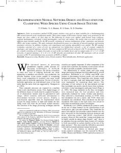
3.1 Node Architecture Each node is an asynchronous circuit and can be divided into three parts: communication logic (4 transceivers), configuration logic and compute logic. The communication logic consists of four transceivers that allow the node to communicate with up to four neighbors on single bit links. Transceivers use a four-phase handshake protocol for data transfer over links. Each handshake transfers one bit, and links support full-duplex data transfer. Each transceiver supports three virtual channels [4] using 1-bit buffers. The four
Transceiver 1
Component
Critical
Description
Configuration Logic
Yes
Input arbitration on VC0, depth first route setup
Transceiver Logic - VC0
Yes
Send/Receive logic for VC-0
Transceiver Logic VC1/VC2
No
Send/Receive logic for VC-1
Point-Point Interconnect
VC0-Yes, VC1/VC2-No
Data interconnect within Node
C
Route Setup Logic
Configuration Logic
Output Buffer
VC0
Mux
DeMux
Instruction Buffer
Transceiver 2
Transceiver 0
Input Buffer
VC0
R S
Opcode
Output Buffer
Register Specifiers D
S
Register File
Routing Entry
Receive Logic
Writing Logic CMD Logic
D
S
Virtual Channel 2
Transceiver 3
Route Logic
Virtual Channel 1
Input Buffer
Point to Point Network
Send Logic
Compute Logic
VC2
Data Buffer
Point to Point Logic
Output Buffer
Control
A L U
VC2
Virtual Channel 0
VC1
Mux
Synch Control Reg
DeMux
Input Buffer
VC1
Analog Control
FIGURE 3. Block Diagram of Node
transceivers are connected to each other and the compute/configuration logic through point-to-point links for each virtual channel. The configuration logic is responsible for setting up internal node routing during the gradient broadcast phase. It configures virtual channel 0 (VC0) for broadcast routing, virtual channel 1 (VC1) for a depth first traversal of the gradient broadcast tree, and virtual channel 2 (VC2) with the reverse routing order of VC1. The computation logic implements a simple two-stage pipeline that allows the execution of instructions on 2-bit data slices. The computation logic has 32 bits of storage configured as a 16-entry 2-bit wide register file and an ALU that can perform simple arithmetic and logic functions. Figure 3 shows the block diagram of a node, clearly identifying the communication, configuration and compute logic. A significant fraction of the node logic is devoted to communication support (both inter-node and intra-node). Next, we examine each logic block to determine its criticality with respect to achieving fail-stop behavior.
3.2 Critical Node Logic We designate a logic block that must be defect free for the node to function correctly as being “critical”. These logic blocks must be tested before a node accepts any external input to avoid the possibility of system misconfiguration. Logic for VC0 (communication logic) and route setup (configuration logic) is critical. All other logic in the node can be tested during the defect isolation phase since it does not affect the ability of a node to receive and send data. While this remaining logic is not critical, it must still be tested to ensure correct functionality. This test can be performed in hardware or in software as part of defect isolation. Table 1 classifies various logic blocks within a node based on their criticality. The classification of logic blocks into critical/noncritical provides a simple way of determining what testing should be performed in hardware, and what can be per-
ALU
No
Arithmetic Logic Unit
Register File
No
Register File in Compute Block
Instruction Buffer
No
First pipeline stage
Execution Control Registers
No
Storage for microinstructions
TABLE 1. Node Component Classification formed with software. Next, we explore different hardware and software test strategies.
3.3 Fail-Stop Node Design Options Our goal is to achieve fail-stop behavior in nodes with minimal extra hardware. Critical logic must be tested before a node communicates with its neighbors, which implies the need for hardware test logic. For non-critical logic, we can choose between three options: a) hardware test, b) hardwaresoftware hybrid test, and c) software test.
Hardware Test. We can add logic to each node to test the functionality of all components. This is equivalent to implementing built-in self-test (BIST) [1,9] that does not require external test vectors. The primary advantages of hardware testing are low latency and the ability to test the node independent of the rest of the system. However, the size of a node that incorporates hardware test circuitry would exceed technological size constraints. This makes a hardware test strategy impractical. Note that critical logic still requires hardware testing.
Software (external) Test. For all non-critical logic, we could rely on software based testing, using externally generated test vectors. This can be combined with gradient broadcast to allow parallel testing of nodes, which would reduce test latency. This approach works well for instruction execution logic, but is not as useful for other components. For example, software testing of the transceiver circuitry for VC1 requires hardware support to allow the routing of test vectors to the transceiver logic. For small logic blocks, this additional hardware could be more expensive than implementing a test scheme in hardware.
FIGURE 4. Transceiver logic for one virtual channel. (Test logic shown in the dotted rectangles is shared between virtual channels)
Hardware/Software Hybrid Test. The final option for testing, is to use a hybrid approach of hardware testing for simple components, and software testing for more complex components. For example, transceiver logic is simple, and requires identical testing for all three virtual channels. This can be done efficiently with simple test hardware. Furthermore, this test hardware can be shared between the three virtual channels. While this could increase test latency by a small amount, it results in reduced circuit size. Compute logic is fairly complex, and requires a large number of test vectors to ensure correct functionality. We can exploit existing hardware to test compute logic using external test vectors, with minimal extra hardware. This allows us to keep node size within technological constraints. In summary, we use hardware test strategies for node components that can be tested with simple logic. We reuse test circuits where possible to minimize the overhead of testing logic. In the next three subsections, we describe our test strategies for the three main components in a node.
3.4 Fail-Stop Communication Logic Communication logic within a node supports three virtual channels and has two primary components: a) four transceivers, and b) point to point links. The circuits for VC0 are part of the node’s critical logic since they are required during configuration. While VC1 and VC2 are not part of critical logic, they can share test logic with VC0. Each transceiver in a node must be tested to ensure correct functionality as defective logic in a transceiver can lead to incorrect system behavior. A node can be a useful part of a
larger system even if it has only one functioning transceiver. However, if there are defective transceivers in a node, it is critical to isolate them from the rest of the system. To achieve this, we augment each transceiver with simple test logic and add a loopback path between the output and input logic of each transceiver. This loopback path is enabled during test only. We exploit the simple four-phase handshake protocol used by the asynchronous logic in designing a test circuit that verifies the operation of the input/output logic. The transceiver is assumed to be defective by default. If the test verifies transceiver operation, the test circuit generates a signal to indicate that the transceiver is operational. The largest component of the test logic is a two-bit state machine which is used to insert a test bit pattern into the transceiver output logic. The test pattern consists of two bits (0 followed by 1). The test logic inserts the 0, then waits until it loops back to the input logic. If the test logic successfully receives the 0 from the input logic, it inserts a 1 and waits for it to loop back. If both data bits (0 and 1) are received correctly, the test logic generates a “TEST_OK” signal. If the data is never received or incorrect data is received, this signal is not generated, isolating this transceiver from the rest of the node. Figure 4 shows the circuit for one virtual channel in a transceiver, along with test logic. In addition to testing the transceiver logic, we need to test the point to point links that connect transceivers. However, routing on the point to point links depends on the result of the configuration process so we test point to point links when we test configuration logic.
3.5 Fail-Stop Configuration Logic
Name
Description
Configuration logic is responsible for determining the role of the node within the system, and for establishing communication routes (inter-node and intra-node). This makes the configuration logic an extremely critical component, and a node cannot function if it is defective. We use a hardware test mechanism that exploits transceiver logic to test the configuration block. Since it uses transceiver logic, the test occurs after the transceiver logic test. The test logic first configures the depth first traversal order of the transceivers within the node, skipping any transceivers that do not generate a “TEST_OK” signal. Next, the test logic uses a two-bit state machine to circulate a pair of bits (0 and 1) on all virtual channels. If the bits are routed correctly, they arrive back at the insertion point due to the loopback path at the transceivers. If the bits are received correctly, the node generates a “CONFIGURATION_OK” signal. To avoid masking defects due to defective route setup, each transceiver must ensure that each bit passes through it only once per VC. The configuration test fails if there is a routing error, the bits never return, or we receive the wrong bit values. A failed configuration test results in a node marked defective.
Our choice of hardware testing for communication and configuration logic, and software testing for compute logic is driven by an analysis of the critical components of a node and technological constraints. As self-assembly technology matures, some of these constraints might reduce enabling the use of other test strategies. Next, we describe how we can exploit the modularity of the node to improve system connectivity and improve tolerance to transistor defect rates.
3.6 Fail-Stop Compute Logic
3.7 Using Partially Functional Nodes
Verifying the compute logic in a node is not as critical as verifying the communication and configuration logic. This is because compute logic does not affect system configuration and a node with defective compute logic can be used to improve network connectivity. However, to ensure that the system generates correct results, the compute logic of each node must be tested. This test can be performed at any point before nodes are organized into larger computational entities. This allows us the flexibility of implementing a hardware test, or a software-based test. In either case, the principle is similar to our previous test strategies - a successful test connects the logic block with the rest of the node. If the test fails, or does not complete, the block remains disconnected from other parts of the node.
In our previous work [7] we assumed that a node could either be defective or working correctly. However, if the probability of failure on an individual transistor is high, a larger number of nodes are rendered unusable. The test logic described earlier in this section opens up the possibility of using nodes with some defective components (if they do not affect system operation). For example, a node with a single defective transceiver can still communicate with up to three neighbors and perform computation. We explore four modes of failure that allow a node to operate with some defective components, defining each scheme based on the number of defects it can tolerate in the compute logic and transceivers. The failure modes are denoted CxTy, where x is the maximum number of defects that can be tolerated in compute logic (0 or 1), and y is the maximum number of defective transceivers that can be tolerated (0,1,2, or 3). The scheme used in our previous work cannot tolerate any defects and is denoted C0T0. The four modes we add are: C0T2 (a node cannot tolerate defective compute logic, but can tolerate up to two defective transceivers), C0T3, C1T2 and a hybrid of C0T3 or C1T2. We list these failure modes in Table 2. Each failure mode tries to include nodes that could contribute to system operation. The difference is in the minimum operating components each node must have to be used by the system. Nodes are considered useful under C0T3 as long as they have one functional transceiver and can be used to compute. Under C1T2 a node is useful as long as it has the potential to improve system connectivity by providing an extra path between two parts of the system (i.e., two active transceiv-
Hardware Test. We can exploit existing logic to allow repeated execution of test instructions to verify the compute logic. However, this test is unlikely to cover all the logic in the compute block without significant extra hardware. Node size constraints and limited test coverage make this test strategy impractical.
Software Test. Software testing can be performed with minimal additions to the existing node logic. Testing of the compute logic must happen before nodes are organized into larger computational entities. We can fold in software testing of the compute block with defect isolation by including the test vectors along with the configuration packet. Another advantage of software testing of the compute logic is the possibility of exhaustive testing to ensure correct operation.
C0T0
Node can tolerate no failures
C0T2
A node can tolerate up to two defective transceivers (compute logic must work)
C0T3
A node can tolerate up to three defective transceivers (compute logic must work)
C1T2
A node can tolerate defective compute logic as well as two defective transceivers
Hybrid
A node can tolerate C0T3 or C1T2
TABLE 2. Node Failure Modes. CxTy defines the number of compute logic (x) and transceiver (y) failures that can be tolerated
ers). The hybrid scheme includes nodes that can either perform computation, or provide an extra path between two parts of the system. As transistor failure probability increases, the number of nodes marked “defective” by each scheme increases. Simulations reveal that this increase is fastest for C0T0, and slowest for the hybrid failure mode. Each node requires extra logic to operate with some defective components. This logic keeps track of defective components in the node and disables the node if the defects cross the failure threshold. For example, the C1T2 scheme requires six bits to keep track of the 6 primary node components (four transceivers, configuration logic, compute logic). In addition, it requires logic that determines if more than two transceivers have failed. While this adds to the size of the node, it allows us to better utilize each node.
3.8 Summary We use a combination of hardware and software test methodologies to verify the operation of a node’s components. We use hardware test logic for critical components, and rely on software testing for other components. A component can be used only if it undergoes a successful test. This results in fail-stop nodes as defective components are isolated from correctly functioning components. Since we use separate tests for node components, with a little extra logic, we can allow nodes to operate even if some (non-critical) components are defective. If transistor reliability is low, allowing these nodes to participate in the system should improve node connectivity. In the next section, we evaluate the effect of using partially defective nodes on the defect isolation mechanism.
4 Evaluation We evaluate three aspects of our proposed scheme. First, we verify that the test logic for communication and configuration is able to detect defects. We also measure the overhead of adding the test logic in terms of the extra transistors required (Section 4.1). Next, we explore the relationship between transistor failure probability and the expected number of defective nodes in the system, in the context of the different modes of node failure (Section 4.2). Finally, we evaluate the benefit of our testing mechanisms by comparing the performance of the defect isolation mechanisms for the different modes of node failure (Section 4.3).
4.1 Test Logic We implement the test logic described in Section 3.4 and Section 3.5 in VHDL and simulate it using the synopsys VHDL debugger. We first verify that the test circuit generates the “TEST_OK” signal in the absence of defects in the circuit within a deterministic delay. Next, we check the response of the test circuit when each signal within the cir-
cuit under test is forced to exhibit stuck-at behavior (i.e., forced to 0 or 1). In each case, we verify that in the presence of a stuck-at fault, the test logic does not return a “TEST_OK” signal. Since the test logic circulates a 0 and 1, we can detect stuck at faults on data lines. Since most data exchanges use handshake signalling, stuck at faults prevent the circuit from making forward progress (the handshakes require changes in the logic level). The test circuits increase the size of the communication and configuration logic by 18% (736 transistors) and 35% (248 transistors) respectively. The overhead for the configuration logic is higher since the original circuit is not very large.
4.2 Node Failure Modes In this subsection, we explore the relationship between the transistor failure probability and node defect rate for different node failure modes (see Table 2). In our previous work [7], we showed that our defect isolation mechanism could tolerate up to 30% defective nodes. In that analysis, we assumed the C0T0 failure mode for a node. To achieve a node defect rate of 30%, the transistor failure probability would have to be less than 4x10⁻⁵. It is unclear if self-assembly can guarantee such low transistor failure probabilities. We can tolerate a higher transistor failure probability by allowing nodes to operate with some defective component. We compute the expected number of defective nodes over a range of transistor failure probabilities, for different failure modes. To study the relationship between per-transistor reliability and node defect rate, we analyze a system with 1 million nodes. Each node is assumed to have 10,000 transistors, with each transistor having the same failure probability (Pf). We use a uniform random number generator to generate random numbers (RND) in the interval [0,1]. Each random number corresponds to one transistor in a node. If RND