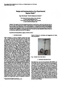
International Conference on Control, Engineering & Information Technology (CEIT’14) Proceedings - Copyright IPCO-2014, pp. 165-169 ISSN 2356-5608
Design and Implementation of a Platform for Experimental Characterization of Static and Dynamic Behavior of Analog-Digital Converters Imen Ben Mansour#1, Raja Maghrebi*2, Nejmeddine Sifi#3 #
University of Carthage, National Institute of Applied Sciences and Technology, INSAT, Research Laboratory « Materials, Measurements and Applications » Dépt. de Génie Physique et Instrumentation, BP676, 1080 Tunis Cedex, Tunisia. 1
*
[email protected] 3
[email protected]
Research Unit in Micro-Electro-Thermal Systems METS, ENIS, Dépt. de Génie Electrique, BP 1173-3038, km 3.5, Sfax, Tunisia. 2
[email protected]
Abstract— This paper presents an implementation of a data acquisition system for analog to digital converters (ADC) using “LabView” as software for data analysis. The designed and implemented platform allows interaction with the device under test (DUT) through means of data acquisition and instrument controls. Developing custom tests in LabView can result in reduced test time, which in turn will help reduce costs in testing. This system was developed for evaluation purposes of ADC's static and dynamic parameters using single and multi-frequency signals. The virtual control and analysis instrument was created in “LabView” environment to control test signals generation and data acquisition. The testing performance of the platform is demonstrated using the classical ADC circuit “ADC0804”. A comparison with experimental results obtained by CANTEST platform from Bordeaux University (France) is also presented. Keywords— Analog-Digital Converter; Static Test; Dynamic Test; LabVIEW Environment; Characterization.
I. INTRODUCTION Analog-to-Digital Converters (ADCs) translate analog electrical signals representing real-world: light, sound, temperature or pressure, to binary numbers. ADCs are key components for the design of power limited systems, in order to keep the power consumption as low as possible. Successive-approximation-register (SAR) analog-to-digital converters represent the majority of the ADC market for medium to high resolution ADCs. There are various methods of finding the code edges of an ADC such as binary search methods that are well-suited for production testing of circuits that are essentially one-bit ADCs like comparators [1]. The use of binary search for ADCs with more resolution will result in at least 100 samples per iteration needed per code edge measurement. Thus, this is not benefit in the test time of production testing. The servo-method is another method that utilizes a servo-circuit that does the function of a step search. This method is a fast hardware version which is very useful for production testing but it is not as fast as the histogram tests like the linear ramp and
sinusoidal methods [1]. In ADC testing, a histogram shows how many times each output code appears in the response vector, regardless of the location [2], [3]. Linear ramp simplifies computation due to the proportionality of the step width to the number of hits of each code [2], [4]. The speed of the ramp cannot be too fast or the code will not be hit as many times as needed in order to get the most resolution and repeatability [5]. In this paper, we choose to use the spectral analysis as a method of ADCs characterization due to the relative ease of producing a pure sinusoidal waveform than a perfectly linear ramp for improved characterization of dynamic performance of the ADC under test [1]. To achieve this goal, we designed and implemented an ADCs characterization platform based upon a high performance data acquisition card and an analysis program using “LabView” programming environment. This analysis program provides all static and dynamic parameters of the ADC under test. II. SAR CONVERSION PRINCIPLE The principle of the successive approximation register (SAR) consists of a sample-and-hold (S/H) circuit, comparator, digital-to-analog converter (DAC) and a logic control unit. The ADC employs a binary search algorithm that uses the digital logic circuitry to determine the value of each bit in a sequential or successive manner based on the outcome of the comparison between the outputs of the S/H circuit and DAC feedback from an array capacitances [6]. Fig. 1 and Fig. 2 illustrate a block diagram of the successive approximation register and the successive approximation conversion procedure respectively [7]. Notice that four comparison periods are required for a 4-bit ADC. Generally, an N-bit SAR ADC will require N comparison periods and will not be ready for the next conversion until the current one is completed. This explains why these ADCs are power and space efficient, yet are rarely seen in speed-and-resolution combinations beyond a few mega-samples per second (Msps) at 14 to 16 bits. Some of the
International Conference on Control, Engineering & Information Technology (CEIT’14) Proceedings - Copyright IPCO-2014, pp. 165-169 ISSN 2356-5608
reduce noise and harmonic distortion. The mixed nature of ADC requires coexisting on the same PCB three antagonistic elements: a sensitive analog part, sensitive and noisy clock, and a noisy digital part. synchronization
smallest ADCs available on the market are based on the SAR architecture [7].
Clock Generator
Filter
Signal Generator
Filter
ADC
Acquisition Card
PC
Fig. 3 Classical ADC test setup. Fig. 1 Block Diagram for the successive approximation register.
For these reasons, we proposed to optimize the test hardware. We replaced the external signals by generating a software configuration of some I/O of acquisition card. Fig. 4 illustrates the proposed test hardware to characterize A/D converters. Clock
ADC Under test
N
Acquisition Card N
PC + LabVIEW
Fig. 4 The proposed ADC test setup.
Fig. 2 Successive approximation conversion procedure.
III. TEST HARDWARE SETUP Test hardware implementation of analog-digital converters, which are generally fast, present difficulties due to the mixed nature of the component itself and the limitation of the test instrumentation. These difficulties increase with the speed and resolution of the ADC. The configuration of the classical test hardware is given in Fig. 3. A sinusoidal signal is used as input and a square signal is generally used to provide the clock that operates the ADC. Filters may be necessary for the clock and the input signal to
With this configuration, we were able to reduce the effects of noise and external noise from different instruments. ADC receives firstly, a 100 ns pulse width to start conversion. Then, it receives an analog input from the personal computer (PC). Analog signal, will attack the input of the converter under test, after conversion, sends its digital output to PC. The latter will store these digital values to determine static and dynamic parameters. The input voltage and the pulse are generated from a software configuration of some I/O of acquisition card. This configuration is performed using the NI-DAQmx LabVIEW module: • PCI 6052E is the acquisition card of National Instruments used to acquire digital data from ADC and to send it to the PC. • NI BNC-2110 is a connector block which simplifies the connection of analog signals, digital signals and timing I/O.
International Conference on Control, Engineering & Information Technology (CEIT’14) Proceedings - Copyright IPCO-2014, pp. 165-169 ISSN 2356-5608
• “Dual tone” technique ADC 0804 is the converter under test, based on successive approximation A\D converters. Fig. 5 and Fig. 6 present the implemented characterization platform and test hardware setup.
A. “Single tone” technique The principle of this technique is to apply a pure sinusoid input to the converter to perform the spectral analysis. Fig. 7 shows an example of the spectrum obtained for a pure sinusoidal input signal. This technique provides the signal to noise ratio with distortion “SINAD”, the harmonic distortion “THD”, Spurious-free dynamic range “SFDR” and the jitter of A\D converter.
Magnitude dB
0
Fig. 5 Implemented characterization platform.
Frequency Fig. 7 “Single tone” spectral analysis.
B. “Dual tone” technique “Dual tone” technique uses as input, the sum of two sinusoidal signals of frequency F1 and F2 having no harmonic relation between them (F1 ≠ k.F2, k is an integer). This technique allows highlighting all the phenomena of intermodulation induced by the conversion of the composite signal. Fig. 8 shows an example of a spectrum obtained with “dual tone” technique. With this testing technique, it is possible to determine the inter-modulation distortion “IMD” of A\D converters.
Fig. 6 Test hardware setup.
Magnitude dB
0
IV. SPECTRAL ANALYSIS TECHNICAL The idea is to send a sinusoidal signal at the ADC input, apply Fast Fourier Transform (FFT) on a finite length of data and analyze the response of the circuit in the frequency domain [8]. There are two spectral analysis techniques: • “Single tone” technique Frequency
International Conference on Control, Engineering & Information Technology (CEIT’14) Proceedings - Copyright IPCO-2014, pp. 165-169 ISSN 2356-5608
Fig. 8 “Dual tone” spectral analysis.
V. STATIC PARAMETERS EVALUATION Static errors are due to the conversion of analog signals into digital signals (quantization error) and imperfections found on a real A/D Converter. “Single-Tone” technical is implemented on the successive approximation converter to identify static parameters of ADC. Fig. 9 shows the transfer function of the ADC under test (blue curve). This curve shows a slight deviation from the ideal transfer curve (red curve), this is due to the nonlinearity of the converter.
Fig. 11 Integral non-linearity of ADC under test.
In Table 1, are summarized the various static errors obtained by the “Single-Tone” technique. TABLE I TEST RESULTS OBTAINED USING SPECTRAL ANALYSIS.
Fig. 9 Transfer function of ADC under test and ideal ADC.
With the same test, we determined the gain error, the offset error and error integral “INL” and differential non-linearity “DNL”. Fig. 10 and Fig. 11 show the transfer function, “DNL” and the “INL” of the ADC under test.
43.32 1.36E-13 1.06 0.06 0.80 none
SNR [dB] Gain error [LSB] Offset error [LSB] DNL [LSB] INL [LSB] Missing codes
To highlight the results of static test, we compared these measures to CANTEST. The latter is a tester developed at “IXL laboratory in Bordeaux University” [9]. Table 2 compares the error rate differential and integral linearity obtained using the implemented platform and the results published for the CANTEST [10]. Through this table, we notice a slight difference between the rate of DNL and INL obtained by the two testers. The test results showed good DNL and INL values and presents correlation with the datasheet of the ADC published by the constructor. TABLE III COMPARISON BETWEEN THE RESULTS OF MEASUREMNTS ERRORS OF DIFFERENTIAL AND INTEGRAL NON-LINEARITY
Implemented platform CANTEST
Fig. 10 Differential non-linearity of ADC under test.
DNL [LSB] Min Max ∆DNL -0.47 0.06 0.53
INL [LSB] ∆INL Min Max -0.79 0.80 -0.47
-0.81
-1.13
0.19
1
0.67
-0.81
International Conference on Control, Engineering & Information Technology (CEIT’14) Proceedings - Copyright IPCO-2014, pp. 165-169 ISSN 2356-5608
VI. DYNAMIC PARAMETERS EVALUATION We coupled the two testing techniques by spectral analysis in order to extract all of the dynamic parameters of the converter under test. We were able to determine the total harmonic distortion “THD”, “SINAD”, “SFDR”, “DFDR”, the number of effective bits “ENOB” and inter-modulation distortion “IMD”. Table 3 shows the various errors obtained by the spectral analysis “Dual-Tone” test. To highlight these results, we compared the measurements to a study made at Bordeaux I University [3]. Table 4 presents a comparison between results obtained using the implemented platform and the ones published in reference [3]. TABLE IIIII MEASUREMENTS RESULTS OF DYNAMIC PARAMETERS USING “DUAL-TONE” TECHNIQUE.
THD [dB] SINAD [dB] ENOB [bits] SFDR [dBFS] DFDR [dB] IMD [dB]
-43.29 43.32 6.904 -48.16 -63.15 -49.89
THD [dB] SINAD [dB] ENOB [Bits] DFDR [dB] IMD [dB]
REFERENCES [1] [2] [3]
[4]
TABLE IVV COMPARISON OF MEASUREMENT RESULTS OF DYNAMIC PARAMETERS.
Our results -53.29 43.32 6.90 -63.15 -49.89
platform is a combination of hardware and software tools. The analysis technique used is the spectral analysis which is based upon FFT. This technique is commonly used in industry for analog and mixed signal circuits, especially Analog/Digital Converters. This technique consists of two complementary testing parts to identify all static and dynamic parameters of A/D Converters: gain error, offset error, INL, DNL, THD, SINAD, SFDR, DFDR and IMD. The classical ADC0804 converter was used as a case study. The results obtained and compared to those achieved by the CANTEST experimental test system developed at Bordeaux I University (France) are very interesting and encouraging in terms of precision and correlation.
[3]
ε
-54.52 44.65 7.60 -64.48 -55.92
11.22 1.33 0.66 1.32 6.03
The overall obtained results show that the differences between the measurements and analysis results obtained using the implemented platform are very close to the published results using CANTEST and those published in [3].
[5]
[6]
[7]
[8]
[9]
[10]
VII. CONCLUSIONS In this paper, an experimental platform implemented for the characterization of A/D converters is presented. The designed
G. Roberts, F. Taenzler and M. Burns, An introduction to mixed-signal IC test and measurement, 2nd ed., Oxford University Press, 2000. M. Mahoney, DSP-based testing of analog and mixed-signal circuits, Wiley-IEEE Computer Society Press, 1987. D. Haddadi, “Test dynamique des convertisseurs analogiques numériques rapides: caractérisation par analyse temporelle, test industriel et considérations instrumentales,” Doctoral Thesis, Graduate School of Physical Sciences and Engineering of Bordeaux I, Bordeaux, France, Dec. 2002. S. Cherubal, A. Chatterjee, “Optimal linearity testing of analog-todigital converters using a linear model,” IEEE Transactions on Circuits and Systems – I. Fundamental Theory and Applications, vol. 50, pp. 317-327, Mar. 2003. B. E. Franklin, C. M. Akujuobi, and W. Ali, “ADC Automated testing using LabVIEW software,” in Proc. of the 2004 American Society for Engineering Education Annual Conference, 2004. F. Azaïs, S. Bertrand, Y. Bertrand, and M. Renovell, “Implementation of a linear histogram BIST for ADCs,” in Proc. Conference on Design, Automation and Test in Europe, Munich, Germany, 2001. H. A. Hassan, I. Abdul-Halin, I. Bin-Aris, and M. K. Bin-Hassan, “Design of a low power 8-bit SAR-ADC CMOS,” in Proc. Student Conference on Research and Development, SCOReD, 2009, UPM Serdang. Malaysia. I. Benamrane, and M. Hamine, “Techniques de Test pour les convertisseurs analogiques/numériques,” Polytechnical School of Montréal, Department of Electrical Engineering, Montréal, Canada, Tech. Rep. 2004. S. Renaud, “Contribution à la caractérisation des circuits de conversion analogique numérique: conception et réalisation d'un système d'évaluation dynamique de ces dispositifs,” Doctoral Thesis, Université de Bordeaux I, Bordeaux, France, 1990. R. Maghrebi, “Contribution à la modélisation, conception et test de structures de conversion analogique numérique,” Doctoral Thesis, National Engineering School of Sfax, Sfax, Tunisia, 2004.