of all components in a form suitable for the architecture of the base devices. This approach is ...... Fig5.1 Building blocks of DS/SS system for FPGA implementation. 5.3.1 Transmitter: ...... Publishing, Allentown, PA, 1998. [79] Z. Navabi, "VHDL: ...
Design and Implementation of Direct Sequence Spread Spectrum System Using Field Programmable Gate Array
A THESIS SUBMITTED TO THE DEPARTMENT OF ELECTRICAL ENGINEERING OF THE UNIVERSITY OF TECHNOLOGY IN PARTIAL FULFILMENT OF THE REQUIREMENTS OF THE DEGREE OF DOCTOR OF PHILOSOPHY IN ELECTRICAL ENGINEERING
BY
HIKMAT NAJEM AL-SHAMARY ( M. Sc.)
June 2004
1
ABSTRACT
Direct sequence spread spectrum communication system have played an outgrowing role in modern communication systems for both military and civil applications due to its unique features. In this thesis, a direct sequence spread spectrum communication system (DS/SS) is designed and implemented using MATLAB-Simulink and then using Xilinx FPGA devices. Firstly, a MATLAB-Simulink tool is used to for designing and implementing DS/SS system to obtain system parameters and to test the influence of signals in the system. For this purpose, a search/lock control unit (SLCU) is proposed to control the synchronization process. Secondly, the logic description of each component in the DS/SS system is derived for the purpose of the FPGA implementation. The direct implementation of these logic descriptions requires high cost of FPGA gate resources and hence the implemented system would operate at low speed. A set of proposals is suggested to reduce the required FPGA implementation cost at the same speed or less. Using these proposals, a DS/SS system in the presence of data modulation (well known problem in DS/SS system) is implemented over Xilinx-virtex FPGA platform. The proposals related to transmitter implementation are: 1- The use of SRL16E marco to implement spreading code. 2- The use of quadrature symmetry of cosine lookup table of binary phase shift keying modulator. The proposals related to receiver implementation are:
2
1- New detection/acquisition scheme is proposed. The scheme uses only the sign bit of digital DS/SS signal to extract the transmitted data and to obtain decision about the synchronization status. This scheme yields to reduce 8bit× 8bit multiplications to just 1bit ×1bit multiplications and to overcome the implementation of the predetection filter. 2- The tracking loop is replaced by simple decision device with an accuracy depends on the sampling frequency. 3- Addition process is partitioned to a set of partial additions to reduce overall adder cost. The simulation results obtained from Model-Sim SE/EE PLUS 5.4a indicate that the proposed detection/acquisition scheme operates efficiently
at
moderate
values
of
signal-to-noise
ratio.
The
implementation reports obtained form Xilinx Foundation ISE4.1 show that : the proposed implementation reduces the cost of transmitter in terms of FPGA cells by 75% with the same delay and the cost of receiver by 95% with 50% reduction in delay.
3
S U P r R V I S O R CFRTIFICATF
I ccttify that this thesis h a s been prepared University o f Technology
under m y supervision at t h e
i n t h e D e p a r t m e n t o f Electrical a n d Electronic
l.^ngincering as a partial r c q u i r c m c n l for tlie degree o fD o c t o r o f P h i l o s o p h y in C o m m u n i c a t i o n
Engineering.
Signature: Name : Dr. Walid. A . Mahmoud (Professor) D a t e : \ll
{0 / 2 0 0 4 .
EXAMINATION C O M M I T T E E C E R T I F I C A T E
Wc
ccilify thai \vch a v e read this ihesis a n d , as a n E x a m i n a t i o n
C o m m i t t e e , examined t h e student i n itscontent a n d i n w h a t is related w i t h i t , and that i no u r o p i n i o n , i t meets t h e standard o f a thesis f o r t h e degree o f Doctor o f i'hilosophy in Communication
Engineering.
Signature:
Signature:
N a m e : D r . R . S. Fyath Professor (Chairman)
Name : Dr. Walid. A . Mahmoud Professor (Supervisor)
Date :/? / /
D a t e -.11 no
2004
/2004.
S ignatUrfi;_----f
Signature:
N a m e : D r . A l i Abfcas A l i Assistant Professor ( M e m b e r ) D a t e : l5//^'^/2004
Name : Dr.Muhammed H.A l i Assistant Professor ( M e m b e r ) D a t e : (^'/ ( o / 2 0 0 4
Siiznaiure:
Signature:
N a m e : D r . A l i Y . Fattah Assistant Professor ( M e m b e r ) Date : / ? //u / 2004
N a m e : Dr. Khamis A . Zidan Assistant Professor ( M e m b e r ) D a t e : i r / /o / 2 0 0 4
Approved forthe Electrical and Electronic Engineering Signature^^^
Department
p^^l^>Bd. Fig2.2 illustrates the waveforms at different stages of the transmitter and receiver in time and frequency domains. In this figure the effect of noise
14
and interference (jamming), in the channel, on the transmitted waveform shape does not considered. The ratio of signal bandwidth to the message bandwidth is called the processing gain (PG) which is an important parameter in specifying the performance of spread spectrum signal in the presence of interference [3,10,30]
PG =
B ss Bd
Κ Κ (2.2)
Assuming that the receiver has synchronized to the transmitter's spreading code, the received signal passes through wideband filter, and is multiplied by a locally generated replica of c(t). Given that c(t)= ±1, then c2(t)=1, and this operation yields to de-spread signal:
φ1 (t ) = 2 S d (t ) cos( ω 0 t + θ )
Κ Κ ( 2 . 3)
at the input to the demodulator. Since ф1(t) follows the definition of a PSK signal, the process of demodulation recovers d(t).
2.3 Pseudo-Noise Sequences for DS Signals: A random binary sequence is a stochastic process that consist of statistically independent symbols (zero or one) called chips, each has a duration Tc. The PN sequence has the properties of random noise. PN sequences are in general easy to generate, the may have long periods, also they should have good correlation properties [3,31]. The PN sequences is usually generated by using a shift register whose contents during each time interval is some linear or non-linear
15
combination of the contents of the register during the preceding time interval. There are many PN sequences that have been developed. These sequences could be divided into two categories [2,30], these are the linear and the non-linear codes. Linear codes could be simply generated by a linear shift register or a combination of linear shift registers. The linear codes are suitable for interference rejection, ranging, and other spread spectrum applications, and although they are useful in spread spectrum communications, linear codes are not secure [6].
2.3.1 Maximal-length Sequences ( M-sequences): Maximal-length codes are the longest codes that can be generated by a given shift register. The maximal length P for a register of order n, is given by [3]:
P = 2 n − 1 chips
Κ Κ ( 2 .4 )
M-sequences may be generated by using linear feedback shift register as shown in Fig2.3.
2.3.2 Gold codes: Gold codes were invented in 1967 at the Magnavox Corporation specifically for multiple access application s of spread spectrum communications [3,32]. Large sets of Gold codes exists which have well controlled cross-correlation properties.
16
Mod-2 Addition
1
2
3
----
n-1
n
Code Output
Fig2.3 order-n M-sequence generator
Gold codes are generated by modulo-2 addition of a pair of maximal linear sequences as shown in Fig2.4. The cross-correlation between the codes is uniform and bounded. Hence, they are used in code division multiple access (CDMA).
2.3.3 JPL Codes: The JPL (Jet propulsion Laboratory) ranging codes are constructed by modulo-2 addition of two or more maximal linear sequences whose lengths are relatively prime to one another [2,3,31].
code1
P1=2n-1 bits
LFBSR1 clock
Gold code=code1+code2 P=2n-1
code2 LFBSR2 P2=2n-1 bits
Fig2.4 Gold code generator configuration
17
Fig2.5 shows a typical JPL code generator configuration, which has three basic maximal-length shift register generators each with a different number of stages. This configuration is identical to the Gold code except for the difference in individual code length. Other composite code such Bent, Kasami, JEFF, Walsh and Barker sequences could be found in [31,33-38].
code1
P1=2m-1 bits
LFBSR1
code2 clock
P2=2n-1 bits
JPL code=code1+code2+code3 P=(2m-1).( 2n-1).( 2r-1)
LFBSR2
code3
P3=2r-1 bits
LFBSR3
Fig2.5 Typical JPL code sequence generator configuration.
2.3.4 Nonlinear Codes: These codes are used for highly security communications purposes, since it is very hard to jammers or eavesdroppers to obtain a complete knowledge about these code, and they are not to generate a replica. This increase in security is achieved by increasing hardware complexity.
18
2.4 Receiver Performance in the Presence of Interference [3,6,39,40]: One of the major properties of all spread spectrum systems is their ability to reject interference. In a properly synchronized receiver, DS signal is despreaded by multiplying it (i.e. correlation) with a locally generated PN sequence replica. This will reduce the signal bandwidth to the message baseband bandwidth, as shown in Fig2.6. On the other hand, a jammer with an incident power equal to J and a bandwidth of BJ is spreaded so that the jammer power spectral density (SJ) at the correlator output is equal to the following:
J ( B J + BSS )
SJ =
Κ Κ (2.5)
The above expression clearly shows that a relatively narrow band jammer is the most effective interference to a direct sequence receiver, since it is typically able to place a great fraction of incident jamming power in the baseband of the victim receiver during communication, than is a relatively wider band jammer [3,41]. Fig2.7 shows the effect of the dispreading PN code on the signal and the narrow band interference. The fraction of the bandpass filter is to filter out the noise and interference components lying outside the bandwidth of the desired signal.
19
DS signal correlator output
Interference
Correlator
BPF
Desired signal output plus processed interference
System noise
Local PN sequence Generator
Fig2.6 Direct sequence system model
DS signal
desired signal
Partial band jammer
f
fο
jammer
fο
f
fο
BI
Bss At the correlator input
At the correlator output
At the BPF output
Fig2.7 Jamming reduction at DS-SS receiver
2.5 Autocorrelation Function and Power spectrum of PN Sequence: In order to estimate the performance of a spread spectrum system, it is necessary to know the power spectrum of the transmitted signal and
20
f
the cross-correlation between the different PN code used in spreading the spectrum. A normalized autocorrelation function (ACF) for the spreading code may be defined as [5,42,43]:
T
Ψ (τ ) = lim T →∞
1 ( ) ∫ c ( t ) c ( t + τ ) dt T 0
Κ Κ ( 2 .6 )
For binary sequences, it turns out that Ψ (t ) can be determined relatively by noting that the variable τ is the number of chips by which locally generated sequence is shifted with respect to the transmitted sequence. Then by comparing the two sequences chip-by-chip, the normalized ACF is determined from [32]:
Ψ(τ ) =
No. of agreements− No. of disagreements No. of chips(bits) in the period of sequence
Κ Κ (2.7)
If, for example, equation 2.7 is applied to the code sequence of Fig2.8, it can be noted that for all positions of code shift, from first digit to the 4th digit of shift, there are 7 agreements and 8 disagreements. Thus Ψ(τ) = 1/15 everywhere except for the position of no shift , where, naturally, all digits are in agreement and Ψ(τ) =1. Thus the autocorrelation function is two-valued and repeats generally with the same periodicity as the pseudonoise (PN) code [6,10,41,44]. The power spectrum of PN-code sequence may be expressed as [3]:
S
PN
= Tc[
sin π fT π fT c
c
]2
Κ Κ ( 2 .8 )
where Tc is the duration of one bit(chip) of the sequence. 21
As a result the transmitted signal has a spectrum with (sin x/x)2 shape with the first nulls in the spectrum spaced
4π/Tc radians, which
represents the bandwidth, apart centered at the carrier frequency.
2.6 Partial Autocorrelation: For purpose of rapid synchronization of long codes often requires an estimate of the correlation between received and locally generated codes be made in less than a full code period. Thus the correlation estimate is based on a correlation over a partial autocorrelation function (PACF) of the code.
1
2
1
3
1
4
1
output
1
(a) Tc 1
1
Repets 1
1
0
1
0
1
1
0
0
1
0
0
0
1
1
1
1
0
(b) 1
Ψ(τ)
0
1
2
3
4
5
6
7
8
9
10 11 12
13 14 15 16 17 18 19
20
τ
-1/15
(c)
Fig2.8 Generation and autocorrelation of 4 bit LFSR code. (a) 4-bit LFBSR code sequence generator. (b) generated PN code with period P=24-1=15 chip. (c) autocorrelation function of the code in (b). 22
The discrete partial autocorrelation function of a sequence [Cn] is defined by[6 ]:
Ψ c ( k , k ′, λ ) =
1
λ
k ′+ λ −1
∑
C nC n+k
(2 − 9)
n=K ′
where k is the number of shifts between sequences k' is the window placement (i.e. window beginning) λ is the window size (in chips).. The partial-period autocorrelation is not two-valued and it depends on the window size and window placement. The mean and variance over k' of Ψc(k,k',λ) are useful quantities for the spread spectrum designer. Because of properties of M-sequence [3,10,41,44], the modulo-2 of Co and Ck is another phase Cq of the same M-sequence.
Ψ c ( k , k ′, λ ) =
1
λ
λ −1
∑
C i+ q + k ′
Κ Κ ( 2 . 10 )
i=0
2.7 Synchronization of DS Receiver: The main function of the DS/SS receiver, is to despread the received PN code. In order to despread the received signal, it must be appropriately synchronized. The synchronization requirements are PN code synchronization, carrier synchronization and data synchronization. However the hardest part of above requirements is the code synchronization because the actual PN sequences are long and their rates are high.
23
The synchronization process consists of two parts, initial synchronization (acquisition), and fine synchronization (tracking). Actually, the acquisition process is the most difficult procedure to be achieved in a DS/SS receiver. This process aligns the receiver's local PN code to within half a chip with the received code. The tracking process the reduces the alignment error to a fraction of a chip, and maintains it for the duration of the transmission. The tracking could be accomplished by using a phase locked loop (PLL) [45]. There are many sources of synchronization uncertainty, some of them are: unstable clock frequency, propagation delay, Doppler shift, channel fading as well as random starting time of receiver with respect to transmitter [46].
2.7.1 Acquisition Methods: A variety of techniques are available for spread spectrum signal acquisition. These techniques are, in general, capable of determining the receiver dispreading code phase to within an accuracy of ±0.5 to ±0.25 of a chip. When the code tracking loop is closed, they may therefore be a phase error of ±0.5 chip, which the tracking loop is expected to eliminate. The performance measure of an acquisition scheme is the mean acquisition time Tacq which is the time required to obtain a correct acquisition.
2.7.1.1 Serial Search Acquisition: Serial search acquisition consists of a search, usually in discrete steps, of the possible time alignments of a locally generated PN code relative to a received PN sequence [5,47]. The time uncertainty region is usually quantized into a finite number of search positions or cells. The
24
cells are serially tested until it is determined that a particular cell corresponds to within a fraction of a chip. The step size or separation between cells is typically one-half of a chip [6].
2.7.1.1.1 Fixed Dwell Time Acquisition Scheme: The dwell time (τd) or integration time (λTc where λ0 0 C );
U1:
std_dff_lx Port map ( RESET => asyn_reset , CLOCK => , D=> C , Q => 0 , Q_BAR => 0_bar ); Figure 3.8 Component Instantiation in VHDL
The benefit of using this low level of coding style by instantiating components from a technology library is to offer excellent user customization on the design. However, in order to have some flexibility on technology upgrades and also controls on architecture implementation, RTL coding style is chosen.
52
The software for VHDL language such as Model Sim SE-EE 5.4a has the possibility to give a complete real timing for all signals of components implemented in VHDL code to test the timing of the circuits before converting them to hardware map [82]. The software Xilinx ISE4.1i with its licenses can convert the VHDL code to hardware map. The space report of internal connection for FPGA chip and timing report by using SPICE technique for this map have reached accuracy of 95% from the real hardware timing. The above facilities give the designer the complete information about his design before implementation [83].
53
Chapter Four Simulation of DS/SS System Using MATLAB-Simulink
4.1 Introduction: In order to efficiently design and implement DS/SS system using FPGA technology, it is necessary first to design and implement such system using MATLAB-Simulik [84,85]. MATLAB-Simulink is an attractive simulation tool provides the designer many facilities to fastly design design, implement and test the desired system. Also it gives designer a clear imagination to the system parameters required to the complete the design [86,87]. These information gained from MATLABSimulink implementation will help us to correctly optimize the cost and speed in FPGA implementation. The waveforms and spectra at any point in the system can easily be obtained using MATLAB-Simulink. This will be
necessary for checking a given design. MATLAB-Simulink of
MATLAB package version 6.1 is considered and toolboxes from communication blockset, DSP blockset, CDMA blockset and SimulinkExtras are used.
4.2 DS/SS system MATLAB-Simulink Realization: Fig4.1 illustrates the block diagram of the overall DS/SS system under consideration. It is the same of the general block diagram of Fig2.1 which shows tha basic system components: the transmitter, AWGN noisy channel as well as correlator, demodulator and synchronization subsystem which they all form and receiver. In the following sections a brief description to each system component. 54
Fig4.1 Simulink block diagram of DS/SS system
4.2.1 The Transmitter and the Channel: Fig4.2 illustrates transmitter implementation. The transmitter contains a random binary data generator from communication blockset converted to a bipolar form using unipolar to bipolar converter and PN sequence generator with generator polynomial g(x)=1+x6 also converted to bipolar form as shown in Fig4.3. Both binary data are multiplied (modulo-2 added in case of unipolar format) and then modulated using baseband BPSK modulator from communication blockset. Since modulation is performed in baseband, no RF carrier is present and the signal is detected at receiver using LPF. The DS/SS is then send through noisy channel with preselected SNR and probability density function. For our simulation we select AWGN channel from communication blockset as shown in Fig4.1.
4.2.2 The Receiver: Fig4.1 shows the DS/SS receiver implementation. It consists of active correlator (mixer and LPF from DSP blockset), demodulator
55
(BPSK demodulator and limiter), synchronization subsystem and local PN code generator with variable clock.
Fig4.2 Simulink implementation of DS/SS transmitter
Fig4.3 Simulink implementation to PN code with generator polynomial g(x)=1+x6
4.2.2.1 The Active correlator: Fig4.4 shows the implementation of active correlator. It contains of mixer (product) and LPF from DSP blockset. The received signal is despreaded only when received and locally generated PN codes have the same phase. The bandwith of LPF is data rate. 56
Fig.4.4 Simulink implementation of active correlator
4.2.2.2 The Data demodulator: Fig4.5 shows the components of data demodulator, which are BPSK demodulator and limiter. No coherent detection used here satisfied the requirements of practical systems.
Fig4.5 Simulink implementation of active correlator
4.2.2.3 The Synchronization subsystem: Fig4.6
illustrates
the
implementation
of
synchronization
subsystem. It contains of acquisition, tracking and search/lock control unit (SLCU) subsystems as well as the local PN code controllable clock input (discrete time voltage controlled oscillator VCO). The SLCU is responsible of the following operation: the output of the correlator is compared to with a preset threshold, if the threshold is exceeded no delay is introduced in the local PN code and initial synchronization is declared otherwise, local PN code is delayed by half a chip and acquisition process is repeated. After the occurrence of acquisition the SLCU enables the tracking loop.
57
Fig4.6 Simulink implementation of synchronization subsystem
Fig4.7 shows the implementation of acquisition subsystem. It contains of square law envelope detector and integrator to detect the correlated signal energy at constant test intervals ( called dwell time). The integrator output is compared with a threshold voltage. If the threshold is crossed then the current phase of local PN code is correct and tracking is initiated, otherwise a phase update signal is generated by SLCU for next phase test operation. This acquisition scheme is called serial search
Fig4.7 Simulink implementation of acquisition subsystem
scheme. Fig4.8 illustrate the tracking scheme used. It is called delay lock loop. The implementation shown in fig shows that there are two branches. The common input to the branches is the received DS/SS signal. The second input to the upper correlator (mixer and LPF) is the output of the
58
local PN code generator while the second input to the lower correlator is a delayed version of local PN generator. For our system the second input is taken from the 6th flip-flop in local PN code generator. The energy detected from both branches is subtracted to generate an error signal excites the VCO to correct its local frequency.
Fig4.8 Simulink implementation of tracking subsystem
Fig4.9 shows the proposed implementation of SLCU. The pulse generator generates a very small width pulse at the end of each integration interval to the output of NAND gate is either a HIT (i.e. acquisition declaration pulse) or not, such that new phase replica is tested.
Fig4.9 Simulink implementation of SLCU
59
A T flip-flop (from Simulink Extras) is used to generate an extra clock at each half chip period rather than chip period in case of there is no HIT has been occurred. This is actually done after module-2 adding the VCO output with T flip-flop output. Since the VCO output is a sinusoidal signal a limiter is used to produce square clock signal . This clock is converted to unipolar format to satisfy the requirements of XOR gate which produces the final update signal ( i.e. local PN clock). However, the phase update signal either gives a clock pulse to local PN code at each chip duration ( normal speed ) when acquisition occurs or at half chip duration ( local PN code fast than received code) when acquisition process do not reach its final decision. A control switch in Fig4.1 is used to select the code used in dispreading operation (either from transmitter or receiver) for the purpose of measuring the performance of synchronization system.
4.3 Evaluation Tests of the Simulation: The following simulation results are developed from testing the system model in Fig4.1 with the following specifications: Data rate : 100 Hz PN code rate : 1MHz PN code length : 127 chip Signal-to-Noise ratio : 10 dB Correlation time : 127 µsec Threshold level : 100 µvolt Sampling frequency : 5 MHz Fig4.10 shows the PN code generator output and BPSK modulator output ( i.e. DS/SS signal while Fig4.11 shows the spectrum of binary data and the spectrum of BPSK modulator (i.e. DS/SS signal ). It is clear 60
(a)
(b) Fig4.10 (a) Output of PN code generator (b) Output of BPSK modulator
from this figure that the spectrum of binary data is spreaded due to the mixing with very high speed spreading code. Fig4.12 illustrates the spectrum of DS/SS signal plus noise in the transmission channel. Fig4.13 shows the spectrum at the output of the mixer of correlator circuit at correct and incorrect phases of local PN code generators. Clearly in case of synchronization (i.e. correct phase), we see that the spectrum is despreaded and the noise is spreaded i.e. SNR is maximized. Fig4.14 shows the waveforms of correlator output and integrator output of acquisition subsystem at correct and incorrect phases of local
61
(a)
(b) Fig4.11 (a) Spectrum of binary data (b) Spectrum of DS/SS signal
Fig4.12 Spectrum of DS/SS signal in the transmission channel
62
(a)
(b) Fig4.13 (a) Spectrum at mixer output of the correlator at correct PN code phase. (b) Spectrum at mixer output of the correlator at incorrect PN code phase. PN code generator. From this figure it is clear that a threshold level of 1x10⁻⁴ volt is a suitable choice to declare initial synchronization. Fig4.15 illustrates the output SLCU while acquisition process continuous, we see obviously that extra clock pulses at half chip duration to get new version of local PN code phase. Due to the large correlation time as compared with PN code rate we could not see obviously more than one of such pulses at the oscilloscope screen (in Fig4.15 this pulse occurs at t=1.27x10⁻⁴ sec).
63
Fig.14 (a) Correlator output at correct PN code phase (b) Correlator output at incorrect PN code phase (c) Integrator output at correct PN code phase (d) Integrator output at incorrect PN code phase
Fig.15 SLCU output while synchronization process not completed
Fig4.16 shows the received and locally generated PN sequences before and after the synchronization occurrence. Fig4.17 shows the transmitted and received data after and before the limiter of demodulator circuit when received and locally generated PN sequences have the same
64
Fig.16 (a) Received PN code waveform (b) Locally generated PN code waveform pre-synchronization (c) Locally generated PN code waveform post-synchronization
Fig.17 (a) Transmitted data (b) Output of BPSK demodulator at correct PN code phase before limiter (c) Output of BPSK demodulator at correct PN code phase after limiter
65
phase (i.e. synchronized). Finally Fig4.18 shows the transmitted and received data after and before the limiter of demodulator circuit when received and locally generated PN sequences are out of phase. Clearly from the previous two figures no successful demodulation of is accomplished without the occurrence of synchronization.
Fig.18 (a) Transmitted data (b) Output of BPSK demodulator at incorrect PN code phase before limiter (c) Output of BPSK demodulator at incorrect PN code phase after limiter
66
Chapter Five Design and Implementation of DS/SS Transmitter Using FPFA
5.1 Introduction: After describing, designing, implementing and testing successfully the DS/SS system using MATLAB-Simulink in the previous chapter. We are now ready to fellow the same steps to obtain the DS/SS system using FPGA devices. In this chapter and the next one, the design and implementation of real time programmable DS/SS system using Xilinx FPGA devices is given. This chapter presents the design and implementation of DS/SS transmitter and channel simulator while the next chapter presents the design and implementation of DS/SS receiver. The design flow take the form shown in Fig3.4. The design is entered as VHDL code modules as component in the system and the signal flow between these components using the package Model Sim SE/EE PLUS 5.4a. Each component is designed such that satisfy the required acceptable optimization of the cost and speed when FPGA implemented.
5.2 System Specifications: The specification of the implemented system is as follows: PN code length : 127 chip - maximal length Chip rate : 1 Mchip/sec (clk1) Modulation type : BPSK Carrier duration : one chip
67
Sampling frequency : 6 MHz (clk2) Bits per symbol : 8 bit Data rate : 100 KHz (clk0) Channel : AWGN noisy channel SNR : 5 dB Acquisition method : serial search (proposed) Tracking method : proposed Correlation time : 30 µsec
The specification of any parameter can be changed easily by modifying the VHDL code of the building unit in which the parameter is active. As a testing tool, the waveforms of signals of different system units are illustrated upon describing each unit.
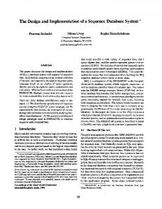
5.3 The Implementation Details: The DS/SS system consists of six main blocks. These blocks are shown in Fig5.1 and labeled : TRANS, NOISE, SIGPLUSNOISE, DETECTOR, LOCALGEN and SYNCH. The block TRANS represent a transmitter transmits 8 bit per symbol BPSK DS/SS signal. The block NOISE is a noise generator generates 8 bit per symbol AWGN while the block SIGPLUSNOISE is an 8 bit adder adds the transmitted signal and noise signal. The block LOCALGEN represent a local generator provides from detector, analyze them and produces a variable clock to local generators to synchronize them with received signal. The DS/SS blocks are implemented using VHDL code is a heretical form. It will be with a main program with sub-routines for its main block. Therefore, these blocks will be continuously divided into sub-sub-routines until final terminal components such as adders and
68
buffers as shown in Fig5.2. The codes of the sub-routine of the block TRANS in Fig5.3 and tpncode in Fig5.4 are examples of the VHDL code that are used.
reset
clk2
reset
clk2
reset
8 bit
TRANS
SIGPLUSNOISE
Data out
DETECTOR clk0
clk1
clk2
8 bit
NOISE
clk3
clk2
reset
LOCALGEN
SYNCH v_clk
clk0
clk2
reset
clk1
reset
Fig5.1 Building blocks of DS/SS system for FPGA implementation
5.3.1 Transmitter: Fig5.5 shows the architecture of transmitter. It consists of random data source, PN code generator, XOR gate and BPSK modulator.
69
5.3.1.1 Random data generator: Since the implementation of random data source is not apart form real DS/SS system but just for test the correct operation of the system, an alternative data source generator is implemented to save the cost of FPGA cells. This means that the data generator is just a buffer for data clock frequency with 1 cell cost. To implement real random data source generator, The digital noise generator discussed in section 5.2.2 may be used.
Fig5.2 The DS/SS program tree.
70
--transmitter.vhd library ieee; use ieee.std_logic_1164.all; use ieee.numeric_std.all; entity transmitter is port(clk0,clk1,clk2,reset : in bit ; din,tcode,d_xor_tcode : out bit; tx_signal : out bit_vector(7 downto 0)); end transmitter; architecture tx of transmitter is component tdatasrce port(clk0,reset : in bit; din : out bit); end component; component tpncode port(clk1,reset : in bit; tcode : out bit); end component; component tbpsk port(a,clk2,reset : in bit; mod_signal : out bit_vector(7 downto 0)); end component; signal t1,t2,t3 : bit; begin c1 : tdatasrce port map(clk0,reset,t1); c2 : tpncode port map(clk1,reset,t2); c3 : t3