cern in low voltage, low power and high performance ap- plications. In this paper .... where CdN is the diffusion capacitance of an NMOSFET. The capacitance of ...
Design and Optimization of Low Voltage High Performance Dual Threshold CMOS Circuits � Liqiong Wei, Zhanping Chen, Mark Johnson and Kaushik Roy School of Electrical and Computer Engineering Purdue University, W. Lafayette, IN 47907-1285 Vivek De Microcomputer Research Labs, Intel Corp., Hillsboro, OR 97124-6461 Abstract Reduction in leakage power has become an important concern in low voltage, low power and high performance applications. In this paper, we use dual threshold technique to reduce leakage power by assigning high threshold voltage to some transistors in non-critical paths, and using lowthreshold transistors in critical paths. In order to achieve the best leakage power saving under target performance constraints, an algorithm is presented for selecting and assigning an optimal high threshold voltage. A general standby leakage current model which has been veri ed by HSPICE is used to estimate standby leakage power. Results show that dual threshold technique is good for power reduction during both standby and active modes. The standby leakage power savings for some ISCAS benchmarks can be more than 50%. 1 Introduction With the growing use of portable and wireless electronic systems, reduction in power consumption has become more and more important in today's VLSI circuit and system designs [1], [2], [3]. In CMOS digital circuits, power dissipation consists of dynamic and static components. Since dynamic power is approximately proportional to the square of supply voltage Vdd and static power is proportional to Vdd , lowering supply voltage is the most e�ective way to reduce power consumption as long as dynamic power is dominant. With the lowering of supply voltage, transistor threshold voltage should also be scaled in order to satisfy the performance requirements. Unfortunately, such scaling can lead to a dramatic increase in leakage current, which becomes an important concern in low voltage high performance circuit designs. Multiple thresholds can be used to deal with the leakage problem. This technique has commonly been used in DRAM chips by raising threshold voltages of the array devices with a xed body bias [5]. For LSI circuits, MultithresholdVoltage CMOS (MTCMOS) circuit technology was proposed
� Acknowledgment: This research is supported in part by DARPA (F33615-95-C-1625), NSF CAREER award (9501869-MIP) & Intel.
to reduce the standby leakage current by inserting high threshold devices in series to normal circuitry [8]. However, the large inserted MOSFETs will increase the area and delay. For a logic circuit, a higher threshold voltage can be assigned to some transistors on non-critical paths so as to reduce leakage current, while the performance is maintained due to the low threshold transistors in the critical path(s). Therefore, no additional transistors are required, and both high performance and low power can be achieved simultaneously. Recently, a dual-Vth MOSFET process was developed [6], which makes the implementation of dual-Vth logic circuits more feasible. However, due to the complexity of a circuit, not all the transistors in non-critical paths can be assigned a high threshold voltage. In order to achieve the best leakage power saving under performance constraints, we present a heuristic algorithm for selecting and assigning an optimal high threshold voltage. A standby leakage model which has been veri ed by HSPICE is used to estimate the standby leakage power of a circuit. The power dissipations of single-Vth and dual-Vth circuits in active mode are also compared using HSPICE simulations. 2 Delay Model 2.1 De nitions A combinational circuit can be represented as a directed acyclic graph G(V; E ). Each node (except for primary inputs and outputs) in the graph maps to a logic gate in the circuit while each edge maps to a path. The propagation delay through node x, denoted as tp (x), de nes how quickly the output responds to a change in the input. The propagation delay of a path �j , denoted as Pd(�j ), is the sum of the propagation delays tp (i) of each node i along this path. It can be expressed as
X
Pd (�j ) = tp(i) (1) The arrival time (Ta (x)) is the propagation delay of each fan-in path of node x. Among all the fan-in paths, there exists a path (or paths) which has a maximum propagation delay value Tmax (x), where Tmax (x ) = i2allmax fT (x)[i]g (2) fanins a The departure time (Tl (x)) of node x is de ned as Tl (x ) = Tmax (x) + tp (x)
th
35 Design Automation Conference ® Copyright ©1998 ACM 1-58113-049-x-98/0006/$3.50
DAC98 - 06/98 San Francisco, CA USA
(3)
VDD 4.5 W =3u eff Leff=0.32u
Vdd=0.6V 4
x
C
n
equivalent on−resistance (k ohms)
y n
C 2 x
x
2 C 1
1
Tox=9.8nm
3.5 V =0.8V dd
3
V =1.0V dd
V =1.2V dd
2.5
Vdd=1.4V
2
1.5
1 0.1
Figure 1: n-input NAND gate R1
1
R2
C1
Rj-1
2 C2
Rj
Cj-1
2.2 Elmore delay model Consider an n-input NAND gate (Figure 1). It can be analyzed using an equivalent RC circuit. Figure 2 shows the equivalent RC circuit of the pull-down network(PDN). The worst case occurs when all Cj 's are discharged simultaneously. Based on the Elmore delay model, the worst case delay (tPHL ) of the PDN is given by
X (C X R ) j=1
j
j
k=1
0.5
0.6
0.7
0.8
Cn
Cj
The path which determines the maximum speed of the circuit is called the critical path. There may be more than one critical path. Critical delay (Tcritical ) is the delay along the critical path.
n
0.4
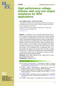
Figure 3: Relationship between RN and V th
n
Figure 2: Equivalent pull-down network of the NAND gate
tPHL = 0:69
0.3
threshold voltage (V) Rn
j
0.2
k
(4)
The capacitance of each internal node j (j = 1 : : : n , 1) in the n-input NAND gate is given as follows, Cj = 2 CdN (5) where CdN is the di�usion capacitance of an NMOSFET. The capacitance of the gate at output is given by Cn = FO (CgP + CgN ) + FI CdP + CdN + FO Cint (6) where CdP is the di�usion capacitance of a PMOSFET. CgP and CgN are the gate capacitances of PMOS and NMOS transistors, respectively. Cint represents the interconnect capacitance per fan-out. FO is the number of fan-outs of the gate, while FI represents the number of fan-ins. For an n-input NAND gate, we have FI = n. Assuming that each NMOSFET has the same on-resistance, the worst-case delay of the PDN can be simpli ed as follows tPHL = 0:69[RN CdN FI (FI , 1) + FI RN Cn ] (7) Although the on-resistance depends on the operation point and varies during the switching transient, we still can make a reasonable approximation by using a xed value. This value is the average of the resistances at the end points of
the transitions [7]. The on-resistance of an NMOSFET is given by R j +R j RN = NMOS Vout=Vdd 2 NMOS Vout=Vdd =2 = 21 ( VIDS jVout=Vdd + VIDS jVout=Vdd =2 ) D D V Vdd dd = k (V , V )� + 2 (8) N dd TN kN [2(Vdd , VTN )Vdd , V2dd ] where VTN is the threshold voltage of an NMOSFET and kN is the gain factor. The constant � is 2 and 1.3 for long channel and short channel MOSFETs, respectively. The relationship between RN and VTN at di�erent supply voltages is shown in Figure 3. For a PMOSFET, the on-resistance(RP ) can be evaluated similarly. For simplicity, we assume that jVTN j = jVTP j = jVth j and RN = RP . For the pull-up network (PUN), the worst case occurs when only one PMOS transistor is \on". The worst case delay (tPLH ) can be expressed by tPLH = 0:69RP Cn (9) The worst-case propagation delay of a CMOS gate is given by tp = (tPHL + tPLH )=2 (10) Following similar procedure, we can get the worst-case propagation delay of the other gates. 3 Standby Leakage Power Estimation In standby mode, the power dissipation is produced by the standby leakage current through each transistor. The leakage current has two sources: reversed-biased diode junction leakage current and subthreshold leakage current. Diode junction leakage is small and can be ignored [7]. Subthreshold leakage exponentially increases with the reduction of threshold voltage, making it critical for low voltage circuits [4]. Therefore, in our simulation, we focus on subthreshold leakage power estimation. In order to estimate standby leakage power accurately, a general transistor model [11], which considers sub-zero gateto source voltage (VGS ) for NMOS and super-zero VGS for PMOS (occurs when multiple series connected transistors
are turned o�), body e�ect and drain induced barrier lowering (DIBL), is used. The following analysis is done for NMOSFETs, but is equally applicable to PMOSFETs. From BSIM2 MOS transistor model [12], the subthreshold current of a MOSFET can be modeled as
Isub = A e n0 kT (VG ,VS ,VTH0 , 0 VS +� VDS ) (1 , e q
,qVDS kT
) (11)
eff ( kT )2 e1:8 . Cox is the gate oxide cawhere A = �0 Cox WLeff q pacitance per unit area. �0 is the zero bias mobility. n0 is the subthreshold swing coe�cient of the transistor. VTH0 is the zero bias threshold voltage. The body e�ect for small values 0of VS is very0 nearly linear. It is represented by the term VS , where is the linearized body e�ect coe�cient. � is the DIBL coe�cient. The standby leakage power of a logic circuit can be expressed as follows [7],
XI
Pstdby = (
i
stdbyi ) Vdd
(12)
where Istdbyi is the standby leakage current through each node i. It depends on the gate topology as well as input signal levels. Let's consider an NAND gate. Assume the transistors which are turned on are short circuits. If all the inputs are \1", the PDN is shorted and the standby leakage current is determined by the PUN. We can get the source and drain voltages of each transistor in the PUN easily. Using equation (11), the leakage contribution of each transistor in the PUN can be calculated separately and added together. If at least one input is \0", the PUN is shorted and standby leakage current is the leakage though the PDN. Suppose there are n transistors which are turned o� in the PDN, the quiescent subthreshold leakage current through each of them must be identical. By equating the leakage current of the transistors in the stack, VS and VDS of each transistor can be obtained. If n = 1, VDS1 = Vdd and VS1 = 0. Otherwise, the following equations can be used 0 dd A1 e q�V n0 kT + 1) (13) VDS2 = q(1 +n2kT ln ( 0 � + ) A2 0 q VDSi = q(1n +kT 0 ) ln(1 + AAi,1 (1 , e, kT VDSi,1 )) (2 < i � n) i
XV n
DSj (1 � i � n) j=i+1 = Vdd , VS1
VSi =
thereby reducing leakage power. However, Figure 3 indicates that a higher threshold voltage will increase the equivalent on-resistance of each transistor, which results in a higher propagation delay. Normally, threshold voltage is empirically de ned to be around 20% of supply voltage to maintain the performance of a circuit [9]. For low supply voltage circuits, the threshold voltage could be very small, leading to a large leakage current. This problem can be circumvented by using dual threshold voltages. A low threshold voltage is assigned to the transistors in critical path(s) in order to achieve high performance, while a high threshold may be assigned to some transistors in non-critical paths to reduce leakage power. The lower bound of low threshold voltage is determined by noise margin. The possible high threshold value should be in the range from low threshold to 0:5Vdd . However, not all the transistors in non-critical paths can be assigned the high threshold voltage. Otherwise, some non-critical paths may become critical. Whether a node can be modi ed depends on the value of the high threshold. If it is too small, there is little di�erence of propagation delay between lowVth and high-Vth transistors. Hence, more nodes can be assigned high-Vth without in uencing the critical delay, but the leakage current improvement for each high-Vth transistor would be small. On the other hand, if the high threshold voltage is too large, the leakage current can be reduced by a large amount for each such transistor. However, fewer nodes can be modi ed. Hence, among the allowable values for high threshold voltage, there exist an optimal one. We developed a breadth- rst search(BFS) algorithm to search for the optimal high-Vth. The rst step in our algorithm is to initialize a circuit with a single low threshold. After initialization, all necessary parameters associated with each node (tp (x), Tmax (x), and Tl (x)) are computed. By checking all the primary outputs and then backtracing, the critical delay and critical path(s) can be identi ed using a rst-in- rst-out (FIFO) queue Q. The pseudo-code for the initialization procedure is shown below. Note that, primary output (PO) does not map to a gate in a circuit, and each PO has only one fan-in gate (fanin(PO)). Initialization () f Assign a level number to each node Calculate the propagation delay tp (x) of each node x Calculate Tmax (x) and Tl (x) of each node x level by level Identify Tcritical by checking the maximum Tl (fanin(PO)) For each primary output PO f If (Tl(fanin(PO)) = Tcritical ) Mark fanin(PO) as a node in critical path Add node fanin(PO) into a FIFO queue Q g While (Q not empty) f Remove node x from Q For each fan-in y of node x f If ((Tl (y) = Tmax (x)) && (y is not a primary input)) Mark x as a node in critical path Add node y into queue Q
(14) (15)
VDS1 (16) where i = 1 represents the top transistor and i = n represents the bottom transistor in the stack. A more detailed derivation of the above equations can be found in [11]. Now equation (11) can be used to calculate the quiescent leakage for any transistor in the stack, which is the leakage current of the PDN. Considering the fact that standby leakage current depends on input signal levels, the average leakage power of a circuit can be evaluated with random patterns applied to primary inputs.
4 Algorithm Due to the exponential relationship between threshold voltage and drain current in the weak inversion region, a higher threshold voltage will signi cantly reduce leakage current,
g
g
g
During the initialization procedure, in order to obtain
Tmax (x) and Tl (x), the circuit has to be levelized. Essen-
tially, levelization assigns a number to each node to indicate the depth of the node in the graph. The level of each primary input is de ned to be 0. The level of any node x, denoted as l(x), can be calculated as follows, l(x) = 1 + j2allmax fl(j )g (17) fanins
High-Vth-Assignment(Vth2 )f For each primary output PO f
Explore each node x using breadth- rst search If x has not been visited Calculate tp (x), Tl(x) and T� (x) for high threshold V th2 if T� (x) � 0 Assign V th2 to x Assign tp (x), Tl (x) and T� (x) for V th2 to x Nc ++ else Keep tp (x), Tl (x) and T� (x) for initial low Vth for x Mark x visited
Ta(x)[i] t p(x) i fanin
x
Tl (x)
.
fanout
y
g
Figure 4: Diagram of a part of a logic circuit where j varies for all fan-in nodes of node x. For each primary input x, tp (x) = 0, Ta (x) = 0, Tl (x) = 0 and Tmax (x) = 0. For each node x in level 1, Ta (x) = 0, Tmax (x) = 0 and Tl = tp (x). Therefore, the parameters (tp (x), Ta (x), Tl (x) and Tmax (x)) associated with each node x can be computed by equations (2) and (3) level by level during the initialization procedure. The next step is to assign a high threshold to some transistors on non-critical paths under performance constraints. This is performed by checking the slack of each node using a BFS-based backtracing algorithm. Slack of a node (T� (x)) denotes the amount by which the gate can be slowed down. For the nodes in critical path(s), slack is 0. For a PO, T� (PO) = Tcritical , Tl (fanin (PO)) (18) For any other node x (suppose x is traversed from node y during back-tracing (Figure 4)), T� (x) can be expressed as T� (x) = minf(T� (y)+Tmax (y),Tl (x)); min(Tmax (z ),Tl(x))g 8z = fanout(x) 6= y (19) where fanin (x) and fanout (x) are the fan-in nodes and fanout nodes of node x, respectively. Consider Figure 4. The rst term in equation (19) ensures that the propagation delay of the path(s): : : : ! fanin(x) ! x ! y ! : : : is no greater than the critical delay. The second term guarantees that the modi cation of the propagation delay of node x cannot a�ect the propagation delay of all the other fanout paths of node x. To make sure that the critical delay is not a�ected, T� (x) is taken as the minimum value of the two terms as shown in equation (19). The procedure for choosing the nodes with a high threshold voltage works as follows. From each PO, BFS is used to explore every node on the breadth- rst tree of G(V; E ). If a node has not been visited yet, by checking its slack, we can decide whether its threshold voltage should be changed. Once the node is visited, it is marked to avoid repeating assignment. By de nition, for each node in a single threshold circuit, its slack(T� ) is no less than 0. Increasing the threshold voltage of a node can result in a higher propagation delay and departure time of this node. Therefore, the slack will decrease. Whether a node should be assigned to a high threshold depends on whether its slack is still positive if its threshold is changed to high threshold. If slack is still positive, this node will be assigned to the high threshold and the number of high threshold NMOS-PMOS pairs (Nc) is incremented. Since the slack of each node in critical path is 0, the threshold voltage of these transistors will not be changed, and hence, the performance is maintained. The pseudo-code for the above procedure is shown below:
g
Finally, we will search the optimal high threshold voltage (opt V th2 ) corresponding to the best saving of standby leakage power. The high thresholds are sampled according to the di�erent on-resistances (R). R(0) is the on-resistance for original low Vth. Step size �R of 0:1R(0) is chosen for the simulation. The relationship between on-resistance and threshold voltage is given by equation (8). Standby leakage power can be evaluated using the method described in section 3. After updating the network for opt V th2 , the circuit can be transfered into SPICE netlist and simulated using HSPICE to verify the results. The procedure is outlined below: Optimal-High-Vth ()f i=1 and R(i) = R(0) + �R Calculate V thi corresponding to R(i) While (V thi < 0:5Vdd)f Initialization High-Vth-Assignment(Vthi ) Estimate standby leakage power Pstdby If standby leakage power is the least power so far Pstdbymin = Pstdby opt V th2 = V thi ++i and Ri = R0 + i � �R Calculate V thi corresponding to Ri g Update network with opt V th2 Transfer the network into SPICE netlist g The above algorithm can be easily extended to solve the other problems, such as multiple supply voltage design & optimization [13]. 5 Implementation and Results The method to reduce leakage power using dual-thresholdvoltage transistors has been implemented in C under the Berkeley SIS environment. In order to simplify the analysis, technology-mapping was used to map the circuits to a library which contains NAND gates, NOR gates and Inverters. All the simulation results were based on a 0:5�m MOSIS process. The e�ective channel length was 0:32�m and the gate oxide thickness was 9.8nm. The e�ective channel widths for PMOSFETs and NMOSFETs were assumed to be 10.5�m and 3�m, respectively. Figure 5 gives an example circuit to show how our algorithm works. Figure 5(a) is the original single-Vth circuit, where the supply voltage is 1V and the threshold voltage is 0.2V. Figure 5(b), (c),and (d) show the dual-Vth circuits with the low Vth of 0:2V and the high-Vth of 0.25V, 0.396V,and 0.46V, respectively. Note that the critical paths and critical delay are maintained after the assignment. Figure 6 shows the standby leakage power of the above example circuit with di�erent high thresholds(V th2 ). The supply voltage is 1V, the low othreshold voltage is 0.2V and the circuit temperature is 25 C. V th2 varies from 0.2V to
0
c d
e
11 00 00 11
c d
h g
b
11 00 00 11
111 000 000 111 011010 11 00 000 111
g
i
l k f
a
a
(a)
d
11 00 00 11
111 000 000 111 011010 11 00 000 111 000 111 000 111 0101 11 00 000 111
111 000 00 11 000 111 01010 11 00 000 111 000 111 00 11 000 111 0101 00 11 000 111 000 111 000 111
j
Circuit Chosen C432 C499 C880 C1355 C1908 C2670 C3540 C5315 C6288 C7552
i
l k f
(b)
111 000 000 111 1 0 11 00 000 111
c
h
b
j
111 000 000 111
Table 1: Optimal High-Vtho and Standby Leakage Power Saving (Vdd =1V, Temp=25 C, Single-Vth:Vth = 0:2Vdd , Dual-Vth: V th1 = 0:2V dd, V th2 =opt-V th2 )
e
e
c d
h g
b
11 00 00 11
e
h g
b
j
j
i
i
l
l
Pstdby (�W )
Gate # 206 532 353 517 615 807 1131 1778 2400 2803
V th2
Pstdby (�W )
(mV ) 333 367 333 333 333 333 367 367 367 367
(1-Vth) 27.97 67.17 46.29 64.86 77.68 106.96 151.18 228.58 355.09 378.95
379.0
0.0
0.0
1.7 1.5 1.4 1.2
55
28
C7
31
C6
C5
54 C3
67
Figure 7: Standby leakage power savings for ISCAS benchmarks (Vdd = 1V )
1.2
80.0
80.0
1.1
High−Vth Transistors High−Vth Gates
20.0
10.0
10.0
0.0
0.0
55 C7
31 C5
54 C3
67
2
20.0
5
30.0
C6 28 8
30.0
0
40.0
0
40.0
8
0.5V (V th2 = 0:2V represents the single low threshold circuit). The squares represent the leakage power obtained by our estimation technique while the circles denote the leakage power obtained by HSPICE simulations. Clearly, the estimation results t well with HSPICE simulation results. The convex point of the curve indicate that there exits an optimal high threshold voltage( 0:396V ) which leads to a 50:67% savings in standby leakage power. Table 1 and Figure 7 show the optimal high threshold and standby leakage power savings for ISCAS benchmark circuits. The percentages of high-Vth transistors and gates over total transistors and gates for di�erent dual-Vth bench-
50.0
90
Figure 6: Standby Leakage power with di�erent V th2
50.0
C2
0.55
5
0.50
35
0.45
C1
0.40
80
0.35
C1
0.30
99
0.25
60.0
C4
0.20
60.0
C4 32
0.7
70.0 Percentage of high−Vth gates and transistors (%)
0.8
Percentage of high−Vth gates and transistors (%)
70.0
0.9
C8
1.0
0.6 0.15
90
C4
Vdd=1V Leff=0.32u Wpeff=10.5u Wneff=3u Tox=9.8nm Temp=25degC
1.6
C2
1.8
32
HSPICE Estimation
1.9
2
63.2
8
63.2
5
126.3
0
126.3
0
189.5
8
189.5
5
2.0
252.6
35
Figure 5: An example circuit (a) 1-Vth Vdd = 1V , V th = 0:2V (b)-(d) 2-Vth Vdd = 1V , Vth1 = 0:2V (b) V th2 = 0:25V (c) V th2 = 0:396V (d) V th2 = 0:46V
252.6
C1
0
80
nodes with high-Vth
C1
nodes with low-Vth
315.8
f
(d)
nodes in critical path(low-Vth)
1−Vth Vth:0.2Vdd 2−Vth vth1:0.2Vdd, Vth2:opt_Vth2
315.8
k
99
a
111 000 000 111
C8
f
(c)
111 000 000 111 000 111 010 0100 11 000 111 000 111 000 111
C4
k
Standby Leakage Power (uW)
a
111 000 000 111
379.0
Standby Leakage Power (uW)
111 000 000 111 000 111 11 00 1 10 0 11 00 000 111 00 11 00 11
Red. (%) 58.51 32.95 61.90 42.73 51.63 48.60 60.25 55.08 21.95 46.96
(2-Vth) 11.60 45.04 17.64 37.14 37.58 54.98 60.09 102.69 277.14 201.01
Figure 8: Percentage of high threshold gates and transistors for dual-Vth ISCAS Benchmarks(Vdd = 1V ) mark circuits are illustrated in Figure 8. In this experiment, supply voltage was 1V and the circuit temperature was 25o C . The low threshold voltage was assumed to be
0.2V and high threshold voltage was the optimal value obtained from our heuristic algorithm given in section 4. Results indicate that the percentage of high threshold voltage transistors can be more than 60% and standby leakage power can be reduced by around 50% for most of the circuits. Even though the optimal high threshold voltage varies for di�erent circuits, for most of the circuits, it was between 0:3Vdd and 0:4Vdd . For a CMOS digital circuit, total power dissipation includes dynamic and static components in active mode. Ignoring power dissipation due to the short circuit current, total active power dissipation can be expressed as follows [10], PT = Pdyn + Pstatic = �i Ci Vi Vdd fclk + IstaticVdd (20)
X i
where �i is the switching activity (the probability of switching), Ci is the load and parasitic capacitances, fclk is the operating frequency and Vi is the voltage swing which equals to Vdd at the output node and Vdd , Vth at internal nodes. The summation is taken over all nodes of the circuit. Istatic is the leakage current through the circuit. Consider the example circuit(Figure 5). Figure 9 shows the HSPICE simulation results of the total active power dissipations of single-Vth and dual-Vth circuits at di�erent frequencies.o The circuits were simulated at 1V supply voltage and 110 C. The threshold voltage of single-Vth circuit was 0.2V. The low and high threshold voltages of dual-Vth circuit were 0.2V and 0.396V, respectively. At low frequency, the active power saving of dual-Vth circuit, which is mainly because of the static power reduction, is about 50%. As for high frequency circuits, the active power dissipation is dominated by dynamic consumption. In addition to leakage power saving, the dynamic power is reduced due to the reduction of internal node voltage swing for high threshold gates. In our example, the total power saving can be around 13% at 100MHz frequency. 10
−4
Active Total Power Dissipation (W)
1−Vth, Vth=0.2V 2−Vth, Vth1=0.2V, Vth2=0.396V
10
−5
Leff=0.32u Wpeff=10.5u Wneff=3u Tox=9.8nm Vdd=1V Temp=110degC 10
−6
10
−1
10
0
10 Frequency (MHz)
1
10
2
Figure 9: Active power dissipation at di�erent frequencies 6 Conclusions In this paper we present a method to design and optimize low voltage dual-Vth CMOS circuits. In order to reduce
leakage power under performance constraints, starting with a single low Vth circuit, a heuristic algorithm for selecting and assigning an optimal high threshold voltage is proposed. For accurate leakage power estimation, a standby leakage current model which has been veri ed by HSPICE simulation is used. Results for ISCAS benchmark circuits show that the leakage power can be reduced by more than 50% under performance constraints. The optimal high threshold voltages are between 0:3Vdd and 0:4Vdd , given that the low threshold voltage is 0:2Vdd . The total active power dissipation can also be reduced using dual-Vth design technique. The total power saving can be about 13% for some circuit at 100MHz frequency. References [1] J. D. Meindl, \Low power Microelectronics: Retrospect and Prospect", Proceedings of the IEEE, Vol.83, No.4, pp.619, 1995. [2] A. P.Chandrakasan, et al.,\Low-Power CMOS Digital Design", IEEE Journal of Solid-State Circuits, Vol.27, No.4, pp.473, 1992. [3] P. Pant, V. De and A. Chstterjee, \Device-Circuit Optimization for Minimal Energy and Power Consumption in CMOS Random Logic Network", DAC, pp. 25.1.125.1.6, 1997. [4] C. Hu, \Device and technology impact on low power electronics", in Low Power Design Methodologies, J.M.Rabaey and M.Pedram, Eds. Norwell, MA:Kluwer,pp21-36, 1996. [5] B. Davari, et al., \CMOS Scaling for High Performance and Low Power-The Next Ten Years", Proceedings of the IEEE, Vol.83, No.4, pp595, 1995. [6] Z. Chen, et al., \0.18um Dual Vt MOSFET Process and Energy-Delay Measurement", IEDM Digest, pp851, 1996. [7] Jan M. Rabaey, \Digital Integrated Circuits", New Jersey: Prentice-Hall, 1996. [8] S. Mutoh, et al., \1-V Power Supply High-Speed Digital Circuit Technology with Multithreshold-Voltage CMOS", IEEE Journal of Solid-State Circuits, Vol.30, No.8, pp. 847-853, 1993. [9] H. Oyamatsu, et al., \Design Methodology of Deep Submicron CMOS Devices for 1V Operation",IEICE Trans. Electron., VOL.E79-C, No.12, pp1720-1724, 1996 [10] A. Bellaouar and M. I. Elmasry, \Low-Power Digital VLSI Design", Kluwer Academic Publishers, 1995 [11] M.C. Johnson, K. Roy, and D. Somasekhar "A model for leakage control by transistor stacking", Technical Report TR-ECE 97-12, Purdue University, Dept. of ECE. [12] J. Sheu, et. al., \BSIM: Berkeley Short-Channel IGFET Model for MOS Transistors", IEEE J. Solid-State Circuits, SC-22, 1987. [13] M.C. Johnson and K. Roy, \Datapath scheduling with multiple supply voltages and level converters", ACM Transactions on Design Automation of Electronic Systems, July 1997.