Design and simulation of an electrically tunable quantum dot cascade laser Dibyendu Dey, Wei Wu, Omer Gokalp Memis, and Hooman Mohseni1 Department of Electrical Engineering and Computer Science Northwestern University, Evanston, IL, USA. ABSTRACT We present here a novel design to form an artificial quantum dot with electrical confinement and apply it to a Quantum Cascade Laser structure to realize a Quantum Dot Cascade Laser. A two-dimensional finite element method has been used to numerically simulate the novel design of electrical formation of an artificial quantum dot. The size of the quantum dot is electrically tunable and can be applied to quantum cascade laser structure to reduce the non-radiative LOphonon relaxation. Numerical modeling with cylindrical symmetry is custom developed using Comsol multiphysics to evaluate the electrical performance of the device and optimize it by varying design parameters, namely, the doping density of different layers and thickness of the cladding and active regions. The typical s-, p-, d- and f- wave functions have been calculated. Numerical simulations show that the energy level separation could be as large as 50 meV by electrical confinement. We also demonstrate the road map for the fabrication of such a device using a maskless super lens photolithography technique. We have achieved a uniform array of nano-contacts of size ~ 200nm, required for the device, using photolithographic technique with a UV source of λ ~ 400nm. The entire processing involves 7 photolithographic steps. This new device - “Quantum dot cascade laser”, promises low threshold current density and high wall-plug efficiency.
Index terms – quantum cascade laser (QCL), quantum dot (QD), quantum dot cascade laser (QDCL), super lens lithography (SLL).
1. INTRODUCTION Quantum Cascade Laser (QCL) is a semiconductor laser that works based on intersubband transition 1. It has already shown room temperature continuous wave operation and high output power in mid-infrared region 2, 3. These emission regions are important resources because they overlap spectrally with the IR sensors that are used to track aircrafts for homeland security. In addition to their use in infrared counter measures (IRCM), they are used in multiple other applications, which include free-space optical communication4, thermal imaging5, bio and chemical gas sensing 6 and pollution monitoring. Recently, much effort has been focused on improving its wall-plug efficiency to make it commercially viable7. Although the general rules of designing the cascade structure are well understood, it is becoming increasingly difficult to improve its wall-plug efficiency further by just redesigning its cascade layer structure. It is because the ultimate performance of QCL still faces the fundamental limitation of wide quantum-well (QW) subband spectrum, corresponding to a free-electronic in-plane motion (motion along the perpendicular direction is quantized by QW potential). The wide spectrum gives rise to a fast non-radiative LO phonon relaxation8, which can be three orders of magnitude faster compared to radiative process. The continuous in-plane spectrum of QWs also results in strong freecarrier absorption and corresponding electrical losses. These lead to a requirement of high threshold current for population inversion. While improvements in the performance capabilities of QCL will no doubt continue, it is necessary to find ways to overcome the limitation of the LO-phonon assisted non-radiative relaxation. It is well known that the LO-phonon relaxation problem can be overcome by converting the QW active region of QCL into a QD array9, 10. Several techniques like applying a magnetic field11, etch and re-growth 12, self-assembly 13, embedding a dot in the cascade structure 14 and exploiting intersubband level transition in quantum dot 15 have been tried to confine electrons. But these methods have intrinsic disadvantages like the structure can be permanently changed in 1
[email protected]; Fax: (847) 491-4455; Phone: (847) 491-7108; bisol.northwestern.edu Nanoepitaxy: Homo- and Heterogeneous Synthesis, Characterization, and Device Integration of Nanomaterials, edited by M. Saif Islam, A. Alec Talin, Stephen D. Hersee, Proc. of SPIE Vol. 7406, 74060Q · © 2009 SPIE · CCC code: 0277-786X/09/$18 · doi: 10.1117/12.825408 Proc. of SPIE Vol. 7406 74060Q-1
etch and re-growth, or spectral gain can broaden due to non-uniformity of the dot size formed by epitaxial growth. The quantum-dot cascade laser we propose here offers the advantage of an intrinsically strong and narrow gain spectrum, with suppressed non-radiative decay with applying lateral electric field.
2. SIGNIFICANCE OF ELECTRICAL CONFINEMENT Energy states in a QW structure are naturally quantized along the growth direction (z-axis) whereas in-plane (x-y plane) energy, states are quasi-continuous. Dimensional transition from QW structure to QDs enhances the in-plane energy separation between states of different sub-bands. Thus, states with in-plane energy difference matching the LOphonon relaxation (ΔE≈30meV) get reduced which helps in decreasing non-radiative electron transition through LO phonon relaxation. As shown in Figure 1(a), an electron in C2 subband can easily relax to any C1 subband state for a QW structure. Figure 1(b) shows that due to unavailability of final states in a QD structure, LO phonon relaxation from C2 subband state to C1 subband state is difficult. As a consequence, the non-radiative LO- phonon assisted electron lifetime in a QD structure is enhanced by a factor of β (lifetime enhancement factor, > 1), which depends on the lateral size of the dot. Effective lifetime for quantum dot cascade laser is enhanced by β times compared to that of conventional QCL. The value of β can be as high as 1516.
Figure 1 – (a) Schematic band diagram of QW structure where electrons can relax between any two points of the subband planes (b) Schematic diagram of the QD structure formed due to electrical confinement. LO phonon relaxation is reduced by splitting subbands further by more than one LO phonon energy of ~ 30 meV
In order to estimate the impact of relaxation-time enhancement factor β on current density, we used a 3 level (|1>, |2>, |3>) rate equation model, where lasing transition occurs between |3> to |2> and phonon relaxation between |2> to |1>. By solving rate equations, we get current density, Jth, of QCL and QDCL and they can be compared by the following expressions –
J th (QCL) =
eLp (α m + α i ) + eng e
−
Δ K BT
(ηinτ 2 − τ 1 )
Proc. of SPIE Vol. 7406 74060Q-2
(I)
J th (QDCL) =
eL p (α m + α i ) + eng e
−
Δ K BT
(II)
(η inτ − τ 1 )
Where, e is the charge of an electron, Lp is the length of cascade stages, αm and αi represent mirror loss and internal loss respectively, ng.exp(-Δ/KBT) represent the density of thermal backfilling electrons, ηin = current injection efficiency, τ2, τ1 represent the life time in the state |2> and |1> and for D-QCL τ represents effective life time. As τ gets much larger than τ2, the threshold current density of QDCL gets substantially reduced.
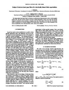
3. DEVICE SIMULATIONS Our novel device is composed of two regions: a small (~ 150-200nm) nano-injection contact (metal) and a gate contact (metal-insulator-metal) which are electrically isolated. The small injection contact serves as the ohmic contact for current injection for the laser and gate contact is used for reverse biasing the Metal-Oxide-Semiconductor (MOS) structure around the injection contact. Both contacts are kept isolated by a thin aluminum oxide layer.
log(n/N)
(a) injector e-
gate
ee-
e-
(b) injector insulator gate
Figure 2 – (color online) (a) 3d cross-section of the FEM simulation on the device structure at injection voltage (Va)=4.5V and Gate voltage (Vg)= −4.5 V showing log (n/N), where n and N represent the electron density and doping concentration respectively. The direction of arrow shows the flow of the electrons. (b) Meshing structure used for the simulation and the dotted line shows the outline of the two-dimensional structure.
When negative bias is applied through gate contact, a high potential region starts to form beneath it. As electrons always prefer to stay in low electric potential region, they move away and start to accumulate below the
Proc. of SPIE Vol. 7406 74060Q-3
injector contact where potential is low due to application of positive injector bias. Such depletion process confines the electrons around the small low potential region below each injector, thus, forming quantum “dots”. The area of electron confinement can be tuned by varying the gate voltage and thus the quantum dot size is electrically tunable 17. The active region is designed to be thin compared to the conventional QCL so that depletion can reach the bottom of active region. Unlike conventional QCL structure, the upper cladding is thin (50nm), low doped InGaAs (3x1016cm-3) and active region consists of 10 active layers (500nm). A 2D finite-element-method (FEM) based model is custom developed using Comsol Multiphysics to evaluate the electrical performance of the device. The model has full 3-D simulation capability and 2-D cross-section modeling capability with cylindrical symmetry. In addition, the simulation tool also incorporates advanced semiconductor models to account for carrier statistics, field dependent mobility, and other non-linear properties. Simulations were done with varying doping concentrations and thickness of active region as well as cladding layers to reach adequate electrical confinement with minimum leakage current. The device with 10 active layers (Si; 5x1016cm-3), 50nm InGaAs upper cladding (Si; 3x1016cm-3) and 500nm InGaAs lower cladding (Si; 3x1016cm-3) gives a good electrical confinement with a low leakage current of 1nA for an applied injection bias of 4.5V and − 4.5V gate bias [Figure 2].
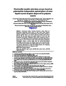
uC [eV] Upper cladding Active region Lowe r c ladding
Figure 3 – 3d potential (uC) on half a cross-section of the device with cylindrical symmetry at an injection bias of 4.5volt and gate bias of –4.5volt. The inserted picture shows the 3-d cross section of the device with the different layer structures.
The FWHM of the harmonic potential at different parts of the active region of the device is calculated at a fixed injection voltage of 4.5V and by varying the gate voltage. As the electrical field confines the electrons over a small region, the shape of the potential gets squeezed and becomes funnel shaped as shown in Figure 3. At a depth of 300 nm of the active region, FWHM gets squeezed up to 24 nm with an applied gate voltage of − 4.5V as shown in Figure 5. It indirectly shows the effect of the gate voltage on the device and the formation of artificial confinement region.
Proc. of SPIE Vol. 7406 74060Q-4
Figure 4 - (video online) A full device performance video, which shows the change of surface potential plot for the device with injection voltage varying from 0 to 4.5 V and gate voltage varying from 0 to − 4.5 V. http://dx.doi.org/10.1117/12.825408.1
90
FWHM [nm]
80
88
z=0
r
Δ ~ 24 nm
z
z=500
70
70 64
60
Δ ~ 20 nm
50 40 30 20
0
100
200
300
Vg =0 Vg =-1V Vg =-2V Vg =-3.5V Vg =-4.5V
50
400
Z [nm] Figure 5 – (Color online) Minimum FWHM of the harmonic potential as a function of the position along the active region, where Z=0 is the top of the active region. The gate voltage is varied from zero to − 4.5V with a fixed injection voltage of 4.5 volt. Inserted picture shows the side view of the device structure.
Using the FEM simulation (Figure 6(a)), we found that the electron energies were shifted due to lateral electrical confinement and the separation between two adjacent energy levels at – 4.5 V gate voltage and 4.5 V injection voltage can be up to ~ 50 meV. It is much higher than the typical LO phonon energy of ~ 30 meV.
Proc. of SPIE Vol. 7406 74060Q-5
Figure 6 – (color online) (a) Electron energy levels of the Quantum well structure after lateral electrical confinement by varying gate voltage. (b) Typical wave functions of structure found by solving Schrödinger equation for the system.
4. WAFER GROWTH The epitaxial layers of the QDCL were grown by low-pressure metal-organic chemical-vapor deposition (MOCVD). The growth conditions were similar to those reported in an earlier letter 18 with the growth rate of the active region set to a low value (0.1nm/s) using double-dilution of precursors. The growth was carried out at a temperature of 650°C and a reactor pressure of 150 Torr using conventional trimethyl reagents - arsine and phosphine - on (100) InP substrate. Figure 7 shows a good match of the experimental and simulated x-ray diffraction curves for the strain compensated QDCL structure.
105
Diffraction Intensity [a.u.]
Simulated
104
Experimental
103 102 101 100 -4000
-2000
0
2000
4000
Relative angle [sec] Figure 7 – (color online) Experimental and simulated x-ray diffraction curves of a 10-period, strain compensated QDCL structure.
Proc. of SPIE Vol. 7406 74060Q-6
5. DEVICE FABRICATION The growth structure was patterned into double trench ridges using standard photolithography with varying ridge widths ranging from 10 to 25 μm. Then, the wafer was deposited with a high quality film of silicon dioxide using plasma-enhanced- chemical- vapor deposition (PECVD). The gas flow rates of SiH4 and N2O were kept to be 40 sccm at a chamber pressure of 200 mTorr, to achieve a slow rate of deposition of SiO2 (10nm/min) at an operating power of 12W. The gate contact was then patterned using lift-off photolithography followed by ebeam evaporation of Ti/Au (20/100 nm) and a thick aluminum (200 nm) . At this stage, we fabricated arrays of nano-holes on the aluminum film using super lens lithography (SLL). The diameter of the hole was as small as ~ 180 nm. SLL is cheap, maskless process compared to the conventional processes like ebeam lithography (EBL) and focused ion beam lithography (FIB). An in-depth study of SLL has been demonstrated previously19,20,21,22. Figure 8 shows the SEM image of the top of the ridge structure of QDCL with the array of nano holes, where each hole forms one quantum dot. As opposing biases are applied to the gate and injection contacts, it is necessary to ensure isolation of the two contacts. Further, the isolation must be good enough to minimize leakage current between the two contacts. To achieve this, a controllable electrical anodization method was used to anodize the surface of the aluminum layer perforated with nano-holes. After anodization, we used dry reactive ion etching (RIE) to anisotropically etch the SiO2 layer inside the nano holes. A recipe of 45 sccm of CF4 and 5 sccm of O2 at 75 mTorr and 60 W power gave a SiO2 etch rate of 20 nm/ min and the anodized aluminum layer was used as the etch mask. This anodization ensured the insulation of the dots from the gate contact as shown in Figure 10. The thickness of the aluminum oxide insulating layer was controlled with the anodization voltage. The aluminum oxide also helped to achieve a very low leakage current (~ nA) and a high break down voltage for the device.
Insulator for separation SiO2 for Gate contact Al MOS
(a)
QW
Injection contact Al2O3 insulator
Depletion
(b) Top view 200nm 500nm
Back contact Figure 8 – (a) Schematic diagram of the QDCL device (b) SEM image of the injector contacts on the ridge of QDCL device formed using super lens photolithography (SLL). Next, the top contact was formed using electron beam evaporation of Ti/Au (20/ 500 nm). The contact metal goes through the holes and makes an injection contact with the device. The sample was rotated during the evaporation of the metal to flow through the tiny holes and ensure a good contact. Finally, a photolithographic mask was used to separate the injection and gate contact layers as shown in Figure 9(a).
Proc. of SPIE Vol. 7406 74060Q-7
Separation between injection and gate contact
(a)
Aluminum Ti/Au gate contact
(b)
Figure 9 – (Color online) (a) Optical image showing the separation being formed between the injection and the gate contacts using photolithography (b) Optical image of the gate contact showing the Ti/Au pad formed over Aluminum layer using photolithography. Figure 10 (a) shows the final device structure after completion of all the fabrication steps. Figure 10 (b) shows the array of quantum dots formed over the QDCL ridge structure.
(a)
Insulator
Injector
(a)
Insulator
Gate Metal
Gate Metal
oxide
oxide
Active region: QW¡¯s Active region 100nm
44μm ?m
(b)
(b)
Figure 10 – (a) SEM image of the device with isolated gate and injection contact (b) SEM image showing array of quantum dots.
Proc. of SPIE Vol. 7406 74060Q-8
6. CONCLUSIONS We have designed a novel technique to form an electrically tunable quantum-dot-cascade laser structure and sketched the basic road map to fabricate it. The preliminary fabrication success has been described while the fully operating device is under testing. Electrical simulations show the formation of an efficient confinement inside the active region enabling formation of artificial quantum dots. The dot size is tunable through varying gate voltage. This method of forming quantum dots is independent of the material structure. Electrical confinement avoids the surface defect states which occur during the etch and re-growth processes. This process also promises a much better uniformity compared to the strain- induced growth technique to form quantum dots. Furthermore, it has the advantage to change the size of quantum dots electrically without harming the lasing process. The method of fabrication is cost-efficient as all the steps involve inexpensive conventional photolithographic processes. Also, the self-aligned nature of the SLL process avoids the risk of electrical short-circuits in such a nano-device. Future work will involve methods to validate the claimed reduction of the density of states due to electrical confinement. Tunneling based approach is one of the methods demonstrated to be capable of accurately measuring the density of states. This method has been previously tested on semiconductor supper lattices 23, semiconductor quantum wires 24, and semiconductor quantum dots 25 and hence can be applied on our device to test the validity of electrical confinement. 7. ACKNOWLEDGEMENT The work is partially supported by Defence Advanced Research Agency (DARPA), under grant # N 00014-07-10564. Some part of the fabrication work was performed at facility of NUANCE Center at Northwestern University. NUANCE Center is supported by NSF-NSEC, NSF-MRSEC, Keck Foundation, the State of Illinois, and Northwestern University.
REFERENCES 1
Faist, J., Capasso, F., Sivco, D. L., Sirtori, C., Hutchinson, A. L. and Cho, A. Y. “Quantum Cascade Laser” Science . 264, 553 (1994) 2 Lyakh, A., Pflugl, C., Diehl, L., Wang, Q. J., Capasso, F.,Wang, X. J.,Fan, J. Y.,Tanbun-Ek, T.,Maulini,R.,Tsekoun,A.,Gao,R. and Patel., C.K.N. “1.6 W high wall plug efficiency, continuous-wave room temperature quantum cascade laser emitting at 4.6 μm”Applied Physics Letter . 92, 111110 (2008) 3 Bai, Y., Darvish, S. R.,Slivken,S., Zhang,W., Evans, A.,Nguyen, J. and Razeghi., M. “Mid-infrared quantum cascade lasers with high wall plug efficiency”Applied Physics Letter. 92, 1011051 (2008) 4 Faist., J. Opt. Photonics. News. “Continious wave room temperature quantum cascade laser” 17, 32 (2006) 5 Hofstetter,D., Beck,M. and Faist., J.”Quantum cascade laser structure as photodetectors”. Applied Physics Letter. 81, 2683 (2002) 6 Bai,Y.,Gokden,B.,Slivken,S.,Darvish, S. R.,Pour,S.A. and Razeghi,M. ”Mid-infrared quantum cascade laser with high wall-plug efficiency” SPIE Proceedings. 7222, 72220O (2009) 7 Razeghi,M. “High performance InP-based Mid-IR quantum cascade laser”. IEEE journal of selected topics in Quantum Electronics. 15, 941 (2009) 8 Bockelmann,U. and Bastard,G. “Phonon scattering and energy relaxation in two-, one-, and zero- dimensional electron gases”Physical Review B, 42, 8947 (1990) 9 Botez,D., Zory, P.and Hsu, C. F.. “Intersubband quantum box semiconductor laser”U. S. Patent 5 953 356. Sept 14 (1999) 10 Wingreen,N. S.and Stafford, C. A. “Quantum dot cascade laser: Proposal for an ultra low threshold semiconductor laser”IEEE Journal of Quantum Electronics. 33, 1170 (1997) 11 Becker,C.,Sirtori,C.,Drachenko, O.,Rylkov,V., Smirnov, D. and Leotin, J.“GaAs quantum box cascade laser”. Applied Physics Letter. 81, 2941(2002) 12 Bhattacharya, P., Ghosh, S. amd Stiff-Roberts, A. D.. “Quantum dot opto-electronic devices”Annu. Rev. Mater. Res. 34,1-40 (2004) 13 Urayama,J., Norris, T.B., Singh, J. and Bhattacharya., P.“Observation of phonon bottleneck in Quantum dot electronic relaxation”Physical Review Letter . 86,4930(2001) 14 Wasserman, D., Gmachl, C., Lyon, C. A. and Shaner, E. A.“Multiple wavelength anisotropically polarized mid-infrared emission from InAs quantum dots”Applied Physics Letter. 88, 191118(2006)
Proc. of SPIE Vol. 7406 74060Q-9
15
Sauvage, S. and Boucaud, P. “Intersublevel polaron laser with InAs/GaAs self-assembled quantum dots”Applied Physics Letter. 88, 063106 (2006) 16 Hsu,C., Seok, J. and Zory, O. P. “Intersubband Quantum-box semiconductor lasers” IEEE Journal of selected topics in Quantum Electronics. 6, 1077 (2000) 17 Mohseni,H. and Chan.,W. “Electrically tunable quantum dots and methods for making and using for same ”U.S. Patent No. 7026641 (2006) 18 Dey,D.,Wu,W.,Memis,O. G. and Mohseni, H. “Injectorless quantum cascade laser with low voltage defect and improved thermal performance grown by metal-organic chemical vapor deposition”Applied Physics Letter 94, 081109(2009) 19 Wu,W., Dey,D., Memis,O. G., Katsnelson,A. and Mohseni, H. “Large areas of nano-perforated holes in multi-stacked metal films by lift-off”. Journal of Vacuum Science Technology B 26, 1745 (2008) 20 Wu,W., Dey,D., Memis,O. G., Katsnelson,A. and Mohseni, H“A novel lithography technique for formation of large areas of
uniform nanostructures”Proc. SPIE, 7039, 70390P (2008)
21 Wu,W., Dey,D., Memis,O. G., Katsnelson,A. and Mohseni, H.” A novel self-aligned and maskless process for formation of highly uniform arrays of nano-holes and nano-pillars” Nanoscale Res. Lett. 3, 123(2008) 22 Wu,W., Dey,D., Memis,O. G., Katsnelson,A. and Mohseni, H.” Fabrication of Large Area Periodic Nanostructures Using Nanosphere Photolithography” Nanoscale Res. Lett. 3, 351(2008) 23 England,P., Hayes, J.R., Harbison,J. P., Hwang,D. M. and Florez., L. T.“Tunneling measurement of density of state of superlattice”. Applied Physics Letter. 53, 391 (1988) 24 Meyer,C., Klijn, J., Morgenstern, M. and Wiesendanger, R.“Direct measurement of the local density of states of a disordered onedimensional conductor ”Physical Review Letter. 91, 076803(2003) 25 Liljeroth,P.,Jdira,L.,Overgaag,K., Grandidier, B., Speller, S. and Vanmaekelbergh.D. “Can scanning tunneling spectroscopy measure the density of states of a semiconductor quantum dot?” Phys. Chem. Chem. Phys. 8, 3845 (2006)
Proc. of SPIE Vol. 7406 74060Q-10