Design Considerations for Area-Constrained In-Pixel Photon Counting in Medipix3 W. Wong, R. Ballabriga, M. Campbell, E. Heijne, X. Llopart, L. Tlustos CERN, 1211 Geneva 23, Switzerland
[email protected] Abstract Hybrid pixel detectors process impinging photons using front-end electronics electrically connected to a segmented sensor via solder bumps. This allows for complex in-pixel processing while maintaining 100% fill factor. Medipix3 is a single photon processing chip whose 55 µm x 55 µm pixels contain analog charge-processing circuits, inter-pixel routing, and digital blocks. While a standard digital design flow would use logic gates from a standard cell library, the integration of multiple functions and configurations within the compact area of the Medipix3 pixel requires a full-custom manual layout. This work describes the various area-saving design strategies which were employed to optimize the use of available space in the digital section of the Medipix3 pixel.
I. INTRODUCTION Medipix3 is a single photon processing hybrid photon detector (HPD) which records the number (as well as the energies) of discrete photons incident on the segmented sensor. It aims to correct the effects of charge diffusion across the sensor volume by considering the total charge collected by all pixels within a local neighbourhood during the evaluation of a charge event. Simulations [1] and a prototype chip [2] have demonstrated that the distortion resultant from charge (of a single event) being shared amongst a cluster of pixels can be corrected by the reconstruction of the total charge into a single pixel. The in-pixel charge summing scheme necessitates complex inter-pixel routing, control logic, and decision-making circuitry. Furthermore, the successful use of the previous chip, Medipix2, in a variety of application fields, such as x-ray imaging [3], x-ray crystallography [4], astrophysics [5], medical instrument prototyping [6], and dosimetry in space [7] and high energy physics experiments [8], has motivated Medipix3 to be made programmable with enriched functionality. Whereas Medipix2 was realized in 0.25 µm technology, Medipix3 is implemented in a 0.13 µm 8-metal layer CMOS process. Although the reduced feature size of the latter technology enables higher transistor density, it was nonetheless challenging to fit the complex processing circuits within the Medipix3 pixel, which maintained Medipix2’s 55 µm pixel pitch. This work explores considerations for designing pixels with high functional density. Section II provides a brief overview of the Medipix3 operation modes and a functional description of the pixel. Section III describes a layout optimization method for area reduction, with a practical example from the Medipix3 pixel. Finally, Section IV presents the conclusions of this work.
II. MEDIPIX3 PIXEL A. Architecture As an HPD, the Medipix3 detector consists of a photosensitive semiconductor sensor (e.g. 300 µm Si) bumpbonded to a front-end electronics chip. To facilitate the user interface, Medipix3 has kept the form factor of its predecessor’s active matrix, with 256 x 256 pixels of 55 µm pitch. Programming of Medipix3 however, will be much more complex than for Medipix2, given the large combination of functional modes and structural configurations. Table 1 lists the operation modes and Table 2 lists the readout modes of Medipix3. Figure 1 shows a block-level description of the pixel’s architecture. The charge, collected from the sensor via the solder bump, is preamplified and then converted to a current. This current is replicated and sent to neighbouring pixels for charge summing and energy threshold discrimination. A winner-take-all routine performs the arbitration to decide to which pixel to assign the photon hit (i.e. the pixel with the largest quantity of charge within the local neighbourhood). Each pixel has two threshold discriminators and two corresponding digital counters, which can be configured as two 1-bit, two 4-bit, two 12-bit counters, or a single 24-bit counter. The two counters/serial shift registers can be programmed to operate simultaneously in the same mode, or can be controlled to operate independently from each other using separate Shutter (Exposure) signals. In continuous read/write mode, the high energy threshold is ignored and the counters take turns counting pulses from the low threshold discriminator, thereby eliminating readout dead-time. When a counter saturates, its value is held at the maximum value for the remainder of the exposure duration (i.e. binary counter overflow is prevented). The counters can also be reset to zero by serially shifting logic-0 through all the bits, or by asserting a FastClear control signal to reset all the bits (within 48 clock cycles). Due to the complexity of the Medipix3 processing circuits, there are almost 1600 transistors in each pixel, which is three times the number of transistors in the Medipix2 pixel.
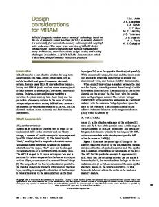
B. Area Constraints While circuit area is an issue for all chip designers, the space available for transistors is particularly constrained in pixels, where layouts are necessarily compact in order to achieve fine granularity. There exists a tradeoff between spatial resolution and functional complexity. Figure 2 shows the layout a Medipix3 pixel.
539
Figure 1: Block-level schematic of the Medipix3 pixel Table 1: Summary of Medipix3 Operation Modes Operation Mode Single Pixel Mode Charge Summing Mode Spectroscopic Single Pixel Mode Spectroscopic Charge Summing Mode
Charge Collection Configuration 1 solder bump per pixel (the sensor is connected to each pixel in the electronics) 1 solder bump per pixel (the sensor is connected to each pixel in the electronics) 1 solder bump per 2x2 pixels (the sensor is connected to each group of 4 pixels) 1 solder bump per 2x2 pixels (the sensor is connected to each group of 4 pixels)
Pixel Size
No. Energy Thresholds per Pixel
Description Each pixel operates independently from its neighbours and processes the charge collected from the sensor via its solder bump. The counters are incremented if the charge is greater than the associated energy threshold. Each pixel considers the total charge from the local 2x2 pixel neighbourhood (110 µm by 110 µm area) for threshold discrimination. The digital hit is assigned to the pixel which received the largest amount of charge from that event.
55 µm by 55 µm
2
55 µm by 55 µm
2
110 µm by 110 µm
8
Each ‘macropixel’ operates independently from its neighbours and counts photons based on the charge collected by its associated solder bump.
8
Each ‘macropixel’ considers the total charge from the surrounding 2x2 ‘macropixel’ neighbourhood (220 µm by 220 µm area) for threshold discrimination. The digital hit is assigned to the ‘macropixel’ which received the largest charge.
110 µm by 110 µm
Table 2: Summary of Medipix3 Readout Modes Readout Mode Sequential Read/Write Semi-sequential Read/Write Continuous Read/Write
Description In the COUNTING STATE, both CounterA and CounterB record the number of photons impinging on the pixel while ShutterA and ShutterB, respectively, are open. In the READOUT STATE, the bits of CounterA and CounterB are serially shifted in turn. CounterA and CounterB can operate in COUNTING STATE or READOUT STATE independently from each other. Note: Only one counter can be serially shifted at a given instant. The counters alternate operations: one counter is in COUNTING STATE while the other is in READOUT STATE. Each pixel effectively has only one energy threshold because both counters record the pulses from the lower threshold discriminator. Readout deadtime is eliminated because one counter is always recording while the other is being read out.
540
would be optimized for at most four transistors in a row. The most area-efficient approach would therefore be to have all transistors along a row share a common active region.
Figure 3: Minimum spacing requirements defined in process design rules of a given technology. a) Active region overlap past the polysilicon. b) Length of the transistor. c) Separation between two transistors on the same active region (with a contact on the common diffusion node). d) Minimum separation between two active regions. e) Separation between two transistors on the same active region (without a contact on the common diffusion node).
Normalized Row Area (µm)
35
Figure 2: Pixel layout
The Medipix3 pixel measures 55 µm on each side. The analog circuits (~220 transistors), occupy 30 µm x 52 µm, while the digital circuits (~1350 transistors), occupy 20.5 µm x 52 µm; the digital circuits are almost 10 times as dense as the analog circuits. The remaining area is reserved for interpixel communication lines, and physical separation between analog and digital circuits/lines to reduce crosstalk.
All transistors on a single active region
30
1-T cells only 1-T, 2-T, and 3-T cells
25
1-T, 2-T, 3-T, and 4-T cells
20 15 10 5
4a
0 1
III. LAYOUT OPTIMIZATION
7
9 11 13 15 17 19 21 23 25 27 29 Number of Transistors
Area rel. to single active region case
180%
A. Design Rule Restrictions
Figure 4 shows the limit on the number of transistors which can fit in a row of transistors. The worst case is to have all transistors lying on discrete active regions (1-T cells only). A 2-input logic gate in a standard cell library would be in the 2-T cell category, i.e. two NMOS (or PMOS) transistors on a single active region. A standard cell library would also contain some complex gates, e.g. OAI, composed of two simple gates. Complex gates would contain three or four transistors in an active region, such that the layout of each cell
5
200%
The Medipix3 pixel has a high transistor density due to the complexity of its functionality. Normally, a standard digital design flow would involve the use of logic gate building blocks from a standard cell library, with the physical layout realized by commercial place and route tools. While this is the most efficient method, it does not achieve the smallest area. To achieve the transistor density necessary to realize the complex processing capabilities of Medipix3, we used a fullcustom manual layout approach.
Figure 3 depicts the minimum sizes and spacing required in the layout of transistors. When adjacent transistors share an active region, the minimum distance between the polysilicon gates is c. When adjacent transistors occupy separate active regions, there is a minimum 2a + d distance between the gates. Since c < a, there a large overhead with respect to area when we place two neighbouring transistors on separate active regions. There is in fact 255% area cost to separate the active regions between adjacent transistors.
3
160% 140% 120%
1-T cells only
100%
1-T, 2-T, and 3-T cells 1-T, 2-T, 3-T, and 4-T cells
80% 60% 40% 20%
4b
0% 1
3
5
7
9 11 13 15 17 19 21 23 25 27 29 Number of Transistors
Figure 4: Minimum area per row of transistors, assuming minimumlength transistors in 0.13 μm technology, minimum spacing between objects, and contacts on all the diffusion nodes. 4b shows that a customized layout, which places as many transistors as possible on a single active region, can result in a layout which is up to 44% smaller than using pre-laid out standard cells.
Clearly, if the two neighbouring diffusion nodes do not share the same signal, then the two transistors must occupy separate active regions. It would therefore be sensible to place transistors which share signal nodes side-by-side so that their active regions may be merged to conserve layout area. This would require that the hierarchy of a circuit block be flattened from the logic gate level to the transistor level.
B. Full-Custom Layout Method Due to the high number of transistors, a full-custom manual layout of a digital circuit is tedious and labour
541
intensive. While Figure 4b showed that it may be possible to save 44% in area by flattening the hierarchy of a circuit block, this strategy can also complicate metal routing. However, the added routing complexity may be the required tradeoff in order to achieve the transistor density necessary to realize the specified functionality within a pixel. The following describes the systematic approach which was used in the full-custom manual layout of the densest sections of the Medipix3 pixel: i)
Divide the overall circuit into major functional blocks of 40-100 transistors.
ii) Draw a flat (transistor-level) schematic for each block. iii) Number each transistor and label each node. iv) Label small squares of paper with the transistor numbers and nodes (each square to represent one transistor). v) Optimize the arrangement of the squares, with the aim to maximize the number of transistors in an active region while aligning gates sharing common signals. vi) Create a circuit floorplan diagram (e.g. Figure 6) to map the circuit. vii) Place and route the transistors following the floorplan diagram. By abstracting the transistors into labeled paper squares, it simplifies the visualization of common nodes and allows the designer to easily manipulate different floorplan arrangements. The floorplan map also makes it possible to keep track of 100 transistors of a flat schematic.
C. Practical Example The following example illustrates the concepts described in the previous sections. Figure 5 shows the logic-gate level schematic of a control circuit used in Medipix3.
Figure 5: Schematic of a control circuit used in the Medipix3 pixel
Figure 6 shows a floorplan diagram of the circuit. This floorplan diagram aids the visualization of shared signal nodes, both between gates and diffusion nodes. This helps to align common signal nodes to reduce the complexity of routing. When the gates are properly aligned, it is also possible to achieve some routing in polysilicon, which can save space at a slight performance cost due to the additional resistance.
Figure 6: A floorplan diagram of the circuit in Figure 5. The transistors are identified by unique numbers (odd numbers represent PMOS transistors and even numbers represent NMOS transistors). The labels on the left, right, and bottom of each rectangle represent the source/drain diffusion nodes and gate node, respectively. The shaded diffusion nodes indicate a node between two transistors in series which does not require a contact. These regions can be extremely useful during routing because they provide flexibility in the spacing between transistors sharing the shaded nodes.
Figure 7 shows the full custom manual layout of the circuit in Figure 5; it follows the floorplanning of Figure 6. For comparison, Figure 8 shows the layout of the same circuit, composed of logic gate cells. The layout depicted in Figure 8 is much more regular and simpler to implement than the layout in Figure 7. The semicustom layout (i.e. Figure 8) would normally be the preferred layout method, provided there is space available. The layout of Figure 7 occupies 34% less area (outlined by the dotted lines) than Figure 8. In the case of Medipix3, the layout of Figure 8 would not have fit and some functionality would have had to be removed from the schematic. Thus, a fullcustom manual layout of flat logic blocks may be necessary in cases where there is not enough area to realize logic gate blocks. There is a practical limit to the number of transistors which can share an active region. Most of the area reductions in a typical circuit would be achieved by grouping together ground (power) nodes. It should be noted that such a strategy could complicate routing, as transistors are not necessarily placed near other transistors belonging to the same logic gate. Scaling down the lateral dimension also reduces the number of available vertical tracks, which further complicates routing. The largest grouping of transistors in the Medipix3 pixel consists of 21 transistors sharing an active region. This occurs along the interface between two counter bits, which is repeated numerously, thus resulting in significant area reduction. Extensive simulations (using both Spectre and static timing) were performed to verify that these full custom digital circuits in the pixel function robustly for up to 200 MHz under best, typical and worst case corner conditions.
542
Figure 7: Full custom layout of the circuit in Figure 5. Left: layout with metal 1, 2, and 3 enabled. Right: the same layout showing only active region and polysilicon so that the placement of the transistors can be clearly seen. This is the layout used in the Medipix3 pixel.
Figure 8: Standard cell, semi-custom layout. Here the circuit of Figure 5 is constructed from logic gate building blocks. The active regions of the blocks are separated by the minimum-allowable distance. Thus, unless these building blocks are combined into complex cells, this is the smallest achievable area using logic gate cells. Left: layout with metal 1, 2, and 3 enabled. Right: the same layout with metal disabled.
IV. CONCLUSIONS In this work, we described the complexity of the photon processing circuits in the Medipix3 pixel. This functional complexity necessitated high digital transistor density, which could be realized using a full-custom manual layout. The Medipix3 design has recently been sent to the fabrication facility. The impact of this level of density on yield will be determined after we test the completed chips.
V. REFERENCES [1] L. Tlustos et al., “Charge sharing in pixel detectors for spectroscopic imaging”, Proc. 9th ICATPP Conference on Astroparticle, Particle, Space Physics, Detectors and Medical Physics Applications, 2005.
[5] J. V. Vallerga et al., “Noiseless imaging detector for adaptive optics with kHz frame rates”, Proc. SPIE Advancements in Adaptive Optics, 2004. [6] M.G. Bisogni et al., “A Medipix2-based Imaging System for Digital Mammography with Silicon Pixel Detectors”, IEEE Trans.Nucl.Sci., 2003. [7] L. Pinsky, J. Chancellor, and D. Minthaka, “Evolving the Medipix2 Technology For Use As An Active Space Radiation Dosimeter”, IEEE Aerospace Conference, 2008. [8] M. Fiederle et al., “Energy calibration measurements of MediPix2”, Proceedings of the 9th International Workshop on Radiation Imaging Detectors, 2008.
[2] R. Ballabriga et al., “The Medipix3 Prototype, a Pixel Readout Chip Working in Single Photon Counting Mode with Improved Spectrometric Performance”, IEEE Trans. Nucl. Sci., Vol. 54, No. 5, 2007. [3] B. Norlin and C. Fröjdh, “Energy dependence in dental imaging with Medipix2”, Proceedings of the 6th International Workshop on Radiation Imaging Detectors, 2004. [4] K. Bethke et al., “Applications and new developments in X-ray materials analysis with MEDIPIX2”, Nuclear Instr. and Methods in Physics Research, 2006.
543