JOURNAL OF SEMICONDUCTOR TECHNOLOGY AND SCIENCE, VOL.17, NO.1, FEBRUARY, 2017 https://doi.org/10.5573/JSTS.2017.17.1.048
ISSN(Print) 1598-1657 ISSN(Online) 2233-4866
Design of a Transceiver Transmitting Power, Clock, and Data over a Single Optical Fiber for Future Automotive Network System Woorham Bae, Haram Ju, and Deog-Kyoon Jeong
Abstract—This paper proposes a new link structure that transmits power, clock, and data through a single optical fiber for a future automotive network. A pulseposition modulation (PPM) technique is adopted to guarantee a DC-balanced signal for robust power transmission regardless of transmitted data pattern. Further, circuit implementations and theoretical analyses for the proposed PPM transceiver are described in this paper. A prototype transceiver fabricated in 65-nm CMOS technology, is used to verify the PPM signaling part of the proposed system. The prototype achieves a 10-13 bit-error rate and 0.188-UI high frequency jitter tolerance while consuming 14 mW at 800 Mb/s. Index Terms—Automotive network, DC balancing, jitter tolerance, phase-locked loops, pulse-position modulation
I. INTRODUCTION Owing to the rapid growth in the number of devices connected to the Internet, the digital data created, replicated, and consumed in the world is increasing explosively. As estimated in [1, 2], the amount of the digital data will double every two years and will be as large as 40 Zettabyte by 2020, while the number of connected devices will be more than 30 billion. The
Manuscript received Oct. 10, 2016; accepted Jan. 15, 2017 Department of Electrical Engineering and Computer Science, Seoul National University E-mail :
[email protected]
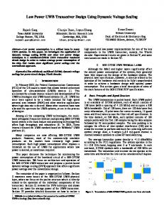
automotive industry will account for a large portion of this trend. In [3], it is expected that by 2025, 100 % of vehicles will be connected to the outside world though a cellular network. Moreover, 75 % of vehicles sold annually around the world will be autonomous by 2035, according to the forecast in [4]. As more and more connected devices are placed in a vehicle, they will create even more data, increasing the need for communication pathways. Automotive networks for infotainment and advanced driving assistance system (ADAS) currently require a communication bandwidth up to hundreds of Mb/s [5]. Media Oriented System Transport (MOST) provides data transmission up to 150 Mb/s for automotive networks using optical fibers. However, it is estimated that the required data rate will reach an era of Gb/s for future vehicles. Serial link technology offers the best solution for high data rate while satisfying the reliability metrics required in automotive applications. To build a highspeed data transmission and recovery system, an additional clock line or a bulky crystal oscillator is required [6]. In [7], a reference-less data recovery scheme was proposed; however, it required a power hungry circuit and a data encoding scheme, which severely degraded the link efficiency. Because the number of links is proportional to that of the connected devices, the wire count and energy efficiency per link should be minimized. Power supply is another important issue. Along with the data transmission wire, an additional power line is used in the legacy automotive network as shown in Fig. 1(a) [8]. As expected in [3, 4], the increasing number of
JOURNAL OF SEMICONDUCTOR TECHNOLOGY AND SCIENCE, VOL.17, NO.1, FEBRUARY, 2017
Head Unit
Battery
MOST Optical Line
Power Line Master Device
Slave Device
Slave Device
(a) Head Unit Optical Line Delivering power/clock/data
Battery PPM Signaling
200 ps
Master Device
Slave Device
Slave Device
implementation for the proposed signaling. Section IV presents the measurement results from a prototype chip. Finally, the conclusion is provided in Section V.
II. PROPOSED ARCHITECTURE
Slave Device
Slave Device
49
Slave Device
Slave Device
(b) Fig. 1. Power and signal lines of (a) the conventional MOST network system, (b) the proposed automotive network system.
devices in vehicles introduces the increase of electromagnetic interference (EMI) and weight of the power line, which causes severe challenges in the legacy metallic powered network [5]. Optically powered networks can be a solution to overcome the aforementioned power line issue [9-11]. In this work, we propose a transmission concept and circuit implementation for transmitting power, clock, and data over a single optical fiber using the pulse-position modulation (PPM) signaling described in [12]. The proposed scheme minimizes the wire count while offering robust data and power transmission. Fig. 1(b) shows the conceptual automotive network incorporating the proposed scheme. A prototype IC for verifying the signaling functionality of the proposed architecture is fabricated in 65-nm CMOS technology. The remainder of this paper is organized as follows. Section II describes the proposed signaling and architecture. Section III gives details on circuit
Along with the optical power delivery technology, which is introduced in Section I, the silicon photonics technology is a promising solution for future automotive networks based on fiber-optic communication. CMOS circuits, such as a vertical-cavity surface-emitting laser (VCSELs) driver, an optical modulator driver, and a trans-impedance amplifier (TIA) developed in prior works [13-15], are very useful for the optically connected automotive networks. The convergence of optical power delivery and silicon photonics can overcome the issues described in Section I; this work proposes a key technology for realizing the convergence. Fig. 2(a) shows the concept of the proposed link for an automotive network. In conventional structures, the data and clock are transmitted over individual wires along with a separate power line. In the proposed structure, the data, clock, and power are transmitted over a single optical fiber. The signaling scheme to realize the proposed structure is shown in Fig. 2(b). When a light with a constant optical power is transmitted, only the power is delivered. If the optical power of the light is altered between two levels periodically, the timing information can also be transmitted. The DC and AC components of the signal can be used as power and clock for the receiver, respectively. Moreover, data can be embedded by modulating the clock, as proposed in literatures [16-18]. The most popular modulation scheme is a so-called clock-edge modulation (CEM), or pulse-width modulation (PWM). In the CEM scheme, only the falling edge of the clock is modulated while the rising edge remains fixed. Therefore, the rising edge provides precise timing information, while the falling edge contains data. However, CEM has a severe drawback, and so is not an ideal method for this proposed automotive link. Because the DC level of the optical signal is used for power delivery, it should optimally be maintained constant-regardless of the data patterns which are being transmitted. However, the DC component of a CEM signal varies with consecutive ones or zeros, as shown in
50
WOORHAM BAE et al : DESIGN OF A TRANSCEIVER TRANSMITTING POWER, CLOCK, AND DATA OVER A SINGLE …
Fig. 4. Block diagram of the proposed PPM modulator.
(a)
Impedance regulator using MN replica VDDPDRV
Impedance regulator using MP replica VDDDRV MP
in
out MN
Pre-driving CMOS buffer
P-over-N VM driver
Fig. 5. Implementation of the output driver.
III. CIRCUIT IMPLEMENTATION
(b) Fig. 2. (a) The proposed link compared to the conventional link, (b) the proposed signaling.
This section focusses on circuit implementation for the data and clock transmission part, based on the prototype transceiver IC presented in [12]. The prototype is composed of a PPM transmitter and a PPM receiver, both of which are integrated in the same chip. In addition to the circuit implementation, a theoretical jitter tolerance of the PPM receiver is derived. A prototype including the optical power delivery part is under development. 1. PPM Transmitter
Fig. 3. Comparison of clock edge modulation and pulse position modulation.
Fig. 3. In contrast, the PPM scheme provides a perfectly DCbalanced signal because the duty-cycle of the clock is not modulated as shown in Fig. 3. For this reason, the PPM scheme is used to embed the data into the clock in this work.
The PPM transmitter consists of a PPM modulator and an output driver. Fig. 4 shows the block diagram of the proposed PPM modulator. A phase-locked loop (PLL) based on a ring oscillator is used to generate a multiphase clock with minimal hardware overhead. A 2:1 multiplexer (MUX) selects one of the clock phases according to the binary data to be modulated into the clock. In order to simplify the design, a 90°-spaced multi-phase clock is used in this work. The binary data which drives the MUX is retimed with the falling edge of
JOURNAL OF SEMICONDUCTOR TECHNOLOGY AND SCIENCE, VOL.17, NO.1, FEBRUARY, 2017
51
(a)
Fig. 6. Proposed PPM demodulator and timing diagram of the demodulator.
clkq to avoid a glitch by placing the data transition in the region where both clki and clkq have a ‘low’ value. A Pover-N voltage-mode (VM) driver is used to provide an output impedance of 50 W and a large voltage swing. The output impedance of the VM driver is calibrated using two replica-feedback impedance regulators described in [19].
(b) Fig. 7. (a) Sampling timing margin of the PPM receiver with a sinusoidal jitter, (b) sinusoidal jitter profile of the PPM receiver.
2. PPM Receiver The main function of the PPM receiver is clock and data recovery (CDR) from the PPM signal. The proposed CDR circuit is composed of a PLL and a flip-flop as illustrated in Fig. 6. The PLL recovers a demodulated clock by averaging the modulated pulse position. Because of the low-pass filtering nature of the PLL, the phase of the recovered clock is located at the middle of the pulse positions of the modulated clock corresponding to ‘1’ and ‘0’. By sampling the modulated clock with the recovered clock, the PPM data can be recovered to the original binary data, as shown in the timing diagram shown in Fig. 6. Because jitter tolerance is the most important performance metric of a wireline receiver, it is necessary to derive an analytic jitter tolerance in a receiver design. The analytic jitter tolerances for an embedded-clock receiver, a forwarded-clock receiver, and a CEM receiver are derived in [20, 6, 16], respectively. In this paper, an analytic derivation of the jitter tolerance of a PPM receiver is described. Fig. 7(a) shows a sampling timing model of a PPM receiver when a sinusoidal jitter is applied to the input. Because the
PLL attenuates the amplitude of the jitter depending on the transfer function of the PLL (HPLL), the recovered clock cannot track the jitter. As a result, the sampling margin is degraded. The jitter profile of a PPM receiver is depicted in Fig. 7(b), where fj, Aj, and Emax denote jitter frequency, jitter amplitude, and maximum timing error, respectively. The timing error that corresponds to the amount of the sampling margin degradation is expressed as J Mclk (t ) - J Rclk (t ) = Aj cos ( 2p f j t ) - | H PLL ( f j ) | Aj cos {2p f j t} .
(1) Because the maximum timing error is occurred when the absolute value of the cosine term is 1, Emax and the condition for an error-free operation becomes
1 Emax = Aj - | H PLL ( f j ) | Aj < UI , 8
(2)
when all the non-ideal conditions are neglected. If we assume that HPLL is a first-order low-pass filter for simplicity, the jitter tolerance is achieved from (2) as
52
WOORHAM BAE et al : DESIGN OF A TRANSCEIVER TRANSMITTING POWER, CLOCK, AND DATA OVER A SINGLE …
Fig. 10. Measured eye diagrams of the PPM signal and the recovered clock. Fig. 8. Chip microphotograph. Jitter Tolerance (UIPP)
100 10 1 0.1 0.01 0.1
Fig. 9. Measurement setup.
4
{ 1+ ( f
j
}
/ f BW ) 2 - 1
,
k 1 + ( f j / f BW ) 2 4
{ 1+ ( f
j
100
(3)
where fBW is a 3-dB cut-off frequency of the PLL. We can introduce a coefficient k (0 < k < 1), which reflects the non-ideal conditions such as a finite signal-to-noise ratio (SNR), a random phase noise, and some datadependent effects. Then (3) becomes as
J P 2 P = 2 Aj