Abstractâ This work presents a new design of a precision voltage reference circuit using MOSFET transistor devices operating in the subthreshold region. Also ...
Design of a Voltage Reference Circuit Based on Subthreshold and Triode MOSFETs in 90nm CMOS Mahmood Mohammed, Khaldoon Abugharbieh, Mahmoud Abdelfattah, Sanad Kawar Electrical Engineering Department Princess Sumaya University for Technology Amman – Jordan Abstract— This work presents a new design of a precision voltage reference circuit using MOSFET transistor devices operating in the subthreshold region. Also, a triode region MOSFET has been deployed instead of using resistors. The circuit has been designed and simulated in 90nm CMOS technology. A reference voltage of 281mV is obtained with Line Sensitivity, LS, of 0.23% in a supply voltage range of (0.8V – 1.65V). The Temperature Coefficient, TC, is 125 ppm/oC, through a temperature range of (0 – 85) oC, The Power Supply Rejection Ratio (PSRR) is -48dB at 50Hz and -26 dB at 1MHz. Finally, the power consumption is 11.31µW and the coefficient of process variations is 0.29%. The design has been simulated using Synopsys Custom Designer and HSPICE CAD tools. Keywords- CMOS; process variation; subthreshold; supply voltage; temperature compensation; voltage reference circuits.
I.
INTRODUCTION
Regardless of circuit techniques and technologies, voltage reference circuits have to generate a reference voltage that varies minimally with process, supply voltage and temperature (PVT) variations. It is an important building block for analog and mixed-signal circuits where precision voltage or current is needed [1]. Because of their critical role in microelectronics, different techniques, technologies and circuit configurations have been applied to achieve such precision voltage. The BJT transistors have been utilized to design voltage reference circuits as in [2], where the I-V characteristics of the BJTs offer an attractive method to overcome PVT variations. But for many reasons, the BJT transistors are replaced by the MOSFET transistors. First, BJTs generate a high reference voltage which requires a high supply voltage. This does not meet the low voltage constraints for modern low power applications [3]. Second, they use resistors which are likely to occupy a large area and consume power [4]. Furthermore, as technology nodes scale down, using bipolar devices becomes unsuitable compared with other techniques such as subthreshold MOSFETs [5], where these technologies require a low supply voltage for proper operation. Due to their capability of exhibiting similar I-V characteristics as BJTs at lower operating voltages, MOSFET transistors operating in the subthreshold region have been used to design voltage reference circuits instead of BJTs. Unfortunately, even though the I-V relation of the MOSFETs in the subthreshold region is similar to the I-V relation of the BJTs, there are three important differences between them. First, the subthreshold current is small due to the large drain-to-source resistance in the subthreshold operation, which would allow a large thermal noise to pass through the circuit. Second, MOSFET devices have intrinsic
978-1-4799-2153-9/14/$31.00 ©2014 IEEE
matching problems that can cause a larger output reference voltage variation than BJT devices. Finally, the drain current, ID, does not have the same temperature coefficient as that of the BJT. Therefore, the temperature coefficient of the voltage reference circuit will be affected [1]. In this work, a new circuit topology has been introduced to design the voltage reference circuit using 90nm CMOS technology. This topology depends on MOSFET transistors which operate in the subthreshold and triode regions. It outperforms other works which deploy similar or scaled-down technologies in terms of their capability to minimize the PVT variations impact on the circuit. The design theory is presented in section II which includes the subthreshold operation and the temperature dependency of the MOSFETs. The new circuit topology is then discussed in section III. Section IV contains design considerations to minimize the PVT variations. The design is simulated in section V, whereas section IV compares these results with previous works in the literature. Finally, section IIV concludes the work introduced in this paper. II.
DESIGN THEORY
A. Subthreshold Operation of the MOSFETs The subthreshold region exhibits similar I-V characteristics as BJTs. It is the region at which the gate-to-source voltage, VGS, is lower than the threshold voltage of the MOSFET, VTH. Equation (1) represents the approximated I-V relation in subthreshold region. 1
μ
exp
(1)
S, which is equal to W/L, is the aspect ratio of the MOSFET device, µ is the carrier mobility and A is a non-ideal factor known as the subthreshold slope given by (2). It depends on the depletion capacitance, CD, and the gate-oxide capacitance, COX. But, CD is always smaller than or equal to COX, which means that 1 ≤ A ≤ 2 [1]. 1
(2)
Finally, VT is the thermal voltage and VTH is the threshold voltage. These two parameters, along with µ, have a temperature dependency. So, they can offer an attractive technique for temperature compensation as will be discussed in the following subsection. B. Temperature Dependency of the Subthreshold MOSFETs Physical characteristics of the MOSFET device generate temperature dependency in the circuits which deploy such devices. As shown in the previous section, VT, VTH and µ are
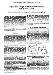
Fig.1: CMOS voltage reference circuit.
the only parameters that depend on temperature, and they are given by (3), (4) and (5) respectively. VT is linearly proportional to absolute temperature, T. KB is the Boltzmann constant and q is the elementary charge. VTH has a linear relation with absolute temperature, T. But VTH decreases as temperature increases, where VTHo is the threshold voltage at 0 K, and k is the TC of VTH [4]. On the other hand, µ is the only parameter that has a nonlinear relation with T, where µo is the mobility at a reference temperature (To). Parameter m is the mobility temperature exponent. The value of m is about 1.5 in standard CMOS technologies [4].
stages: the start-up stage, the current generator stage and the output stage.
(3)
The current, I, which is produced by this stage, can be derived by writing the KVL loop through the transistors M1M5 as in (6).
(4) μ
μ
T
A. PTAT Current Generator Stage
(6) (5)
Temperature properties of VT and VTH offer an attractive technique for temperature compensation since they can cancel the opposite linear dependency on temperature of each other. But, the use of µ for temperature compensation is usually avoided, because of the mobility nonlinear relation with temperature. Due to the existence of VT, VTH and µ, the output voltages and currents in circuits that use MOSFET devices can be classified into two types: Proportional to Absolute Temperature (PTAT) voltage or current and Complementary to Absolute Temperature (CTAT) voltage or current. In order to generate an output voltage or current as independent as possible from temperature, PTAT and CTAT current or voltage have to be generated. Then, they are used to terminate each other as will be discussed in the following sections. III.
The start-up circuit is used to ensure bias in the desired state upon power up. After the reference voltage reaches the desired value, the start-up circuit is disabled automatically. The current stage produces a PTAT current, I, which is injected through the current mirror transistors M6 and M9 in the output stage that has a CTAT reference voltage, VREF. The detailed principle of operation is presented in the following subsections.
By rewriting (1) in terms of VGS, (7) can represent the VGS of the subthreshold transistors. ln
(7)
S
Substituting (7) in (6) for transistors M2-M5, VDS1 can be written as in (8). ln ln ln ln
S
S S
(8)
S
Let Bi = Si µi Cox (A - 1), where i denotes to the transistors, and A is equal for all transistors [4]. So, (8) can be re-arranged as in (9).
CIRCUIT TOPOLOGY
Fig.1 shows a new circuit design to provide a constant reference voltage based on the difference of transistors voltages and through a temperature compensation technique that utilizes the subthreshold operation of the MOSFETs. All transistors in the circuit are operating in subthreshold, except for M1 which operates in the triode region. The circuit consists of three
ln
B B
B I
B
(9)
By simplifying (9) and assuming that µ is identical for all transistors, VDS1 can be written as in (10). ln
(10)
But M1 is operating in the triode region, so I of the transistor M1 is given in (11). Assuming VDS1 is very small, the resistance of M1, RM1, is given by (12), where VA is gate-tosource voltage of M1 as seen in Fig.1. (11) (12)
S
By substituting (10) and (12) into (11), the current I can be written as in (13). S μ
ln
(13)
The expression (VA – VTH1) is equal to (VA – VTHo-1 + kT). However, VA – VTHo-1