Design of a Wide Input Range DC-DC Converter with a Robust Power Control Scheme Suitable for Fuel Cell Power Conversion Maja Harfman Todorovic
Leonardo Palma
Prasad Enjeti
Student Member IEEE
Student Member IEEE
Fellow IEEE
Power Electronics & Fuel Cell Power Conversion Laboratory Department of Electrical Engineering Texas A&M University College Station, TX 77843-3128 Tel: 979-845-7466 Email:
[email protected] ; http://enjeti.tamu.edu
A fuel cell produces a DC voltage from hydrogen-rich fuel gas and air that flow over two cell electrodes. They are similar to batteries in that both produce a direct current by using an electrochemical process. However, unlike batteries, fuel cells can provide the power continuously as long as the reactants are supplied. Since the DC voltage generated by a fuel cell stack varies widely and is low in magnitude (Vcap/2 (as previously described) yielding the duty cycle of
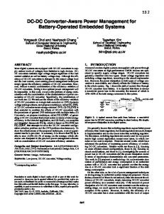
Figure 8. Block diagram of the boost converter control subsystem.
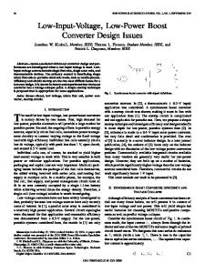
In order to test the performance of the control algorithm for all three scenarios, the system was subjected to a change of load from 5kW to 1kW while limiting the output power of the fuel cell to 2kW indicated by the PA signal. The results of the simulation are presented in Fig. 9.
D = 2 −
2 V in = 0 . 95 . V cap
(7)
The input current is calculated to be 132.3A assuming full power with 90% efficiency. Considering that current is high, we decided to use 100kHz switching frequency in order to reduce the inductor’s core size. Assuming the ripple current level of 5% the needed inductance is L=
V in − 0 .5V cap 2 ∆I
DT S = 2 .87 uH .
(8)
Maximum current ratings of switches Sb1, Sb2 and diodes Db1, Db2 are calculated to be 66A and their voltage rating is Vcap / 2=40Vdc .
(9)
B. Two inductor boost converter design The second stage input voltage is regulated by the three level boost converter to 80Vdc and the output voltage of the converter is to be maintained at 400 Vdc. In this case the transformer turns ratio n1/n2 is chosen to be 1/2. Therefore, from Eq. 2 a duty cycle, which is the overlapping time of the switches S1 and S2 is calculated to be
Figure 9. Ultracapacitor voltage, load power demand, and the power supplied by the fuel cell.
During the high power demand period (Fig.9, region I) a part of the load is supplied by the ultracapacitor, which manifests itself as a voltage drop from 80V to 79.2V on the ultracapacitor voltage plot. Following the load demand decrease, the fuel cell is able to satisfy the entire load and charge the ultracapacitor at the same time (Fig.9. region II). After the capacitor is fully charged the system enters into the normal operation mode (Fig.9. region III) where all requested energy is provided by the fuel cell.
D = 1−
2Vo n1 = 0.16 Vin n2
(10)
The input current of the converter is calculated from the output power and input voltage considering an efficiency of 90%, and it results to be 32.7 A. The switching frequency of
378
converter does not exceed 0.5 times the voltage across the switch. This reduces the possibility of device failure due to an over voltage.
20 kHz for this stage is used in order to minimize switching losses. Then, given an input current ripple of 5%, the required inductor values for L1 and L2 are obtained to be L=
Vin D 1 = 205uH 2 f s I rripple I in
(11)
The maximum ratings of switches S1 and S2 are calculated to be 53A peak for the current and their voltage rating is
Vds = 2
n1 VO = 400 Vdc n2
(12) Figure 11. Current in the coupled inductor T1.
Similarly the voltage rating of the rectifier switches S’1 and S’2 can be calculated to be Vds , rec = 2Vo = 800
VII. CONCLUSIONS
(13)
A step-up DC-DC converter topology using cascaded modules along with a new control strategy has been proposed. Simulation results show that the system has a good performance and proper response under load characteristics. More importantly, the power limiting characteristic of the control scheme gives time to the fuel cell to react on its own dynamics when a sudden load step is applied to the system. A 5kW prototype hardware realization of the system is under construction. The preliminary test results shown in this paper were obtained from a 1kW converter prototype and confirmed the viability of the proposed topology. An overall efficiency of 90% or higher is achievable.
Finally, their current rating is calculated to be 18 A peak. VI. PRELIMINARY EXPERIMENTAL RESULTS The proposed converter and control algorithm are being implemented in a laboratory prototype, which is currently under test. The results shown in the following figures correspond to a preliminary 1kW prototype with a switching frequency of 75kHz. Figure 10 shows the drain to source voltages for switches S1 and S2 of the DC-DC converter when supplying a 750W load under steady state operating conditions. The input voltage of the system during this test was measured to be 40VDC, and the input current of the system was measured to be 22 ADC. Figure 11 shows the current waveforms measured in the coupled inductor T1. As can be seen, two currents in the inductors L1 and L2 in T1 match perfectly thus reducing the possibility of saturation in the transformer T2 due to a current mismatch in the primary winding.
VIII. REFERENCES [1] M. Pagano, L. Piegari, “Electrical networks fed by fuel-cells for uninterruptible electrical supply,” Proceedings of the ISIE, May 2002, Vol. 3, pp. 953-958 [2] E. Santi et al., “A fuel cell based domestic uninterruptible power supply,” Proceedings of the APEC, March 2002, Vol. 1, pp. 605 -613 [3] K. Wang et al., “Bi-directional DC to DC converters for fuel cell systems,” Proceedings of the Power Electronics in Transportation conference, October 1998, pp. 47 -51 [4] C. Liu et al., “Power balance control and voltage conditioning for fuel cell converter with multiple sources,” Proceedings of the PESC, June 2002, Vol., pp. 2001 -2006 [5] M.T. Zhang, Y. Jiang, F.C. Lee, M.M. Jovanovic, “Single-phase threelevel boost power correction converter,” Proceedings of the APEC, March 1995, Vol. 1, pp. 434 -439 [6] B. Linch, K. Hesse, “Under the hood of low-voltage DC/DC converters,” Texas Instruments seminar, http://www.ti.com/seminar [7] J. Yungtaek, M. Jovanovic, “New Two-Inductor Boost Converter with Auxiliary Transformer,” Proceedings of the APEC, March 2002, Vol. 2, pp. 10-14
Figure 10. Converter waveforms for a 750 W output power.
Also from the source to drain waveforms shown in Figures 10 and 11 it can be observed that the voltage stress applied to switches on the primary side of the DC-DC
[8] S. Othsu, T. Yamashita, “Stability in High-Output-Voltage Push-Pull Current-Fed Converters,” IEEE Transactions on Power Electronics, April 1993, Vol. 8, Issue 2, pp. 135 -139.
379