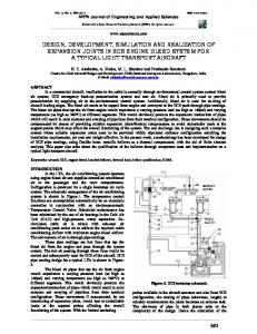
Design, simulation and realization of high power NPC converters equipped with IGCTs A. Zuckerberger, E. Suter, Ch. Schaub, A. Klett, P. Steimer IAS, October 1998, St. Louis, USA
Copyright © [1998] IEEE. Reprinted from the Industry Applications Society.
This material is posted here with permission of the IEEE. Such permission of the IEEE does not in any way imply IEEE endorsement of any of ABB Switzerland Ltd, Semiconductors's products or services. Internal or personal use of this material is permitted. However, permission to reprint/republish this material for advertising or promotional purposes or for creating new collective works for resale or redistribution must be obtained from the IEEE by writing to
[email protected].
ABB Industrie AG
Design, simulation and realization of high power NPC converters equipped with IGCTS
Design, simulation and realization of high power NPC converters equipped with IGCTs A. Zuckerberger, E. Suter, Ch. Schaub, A. Klett, P. Steimer ABB Industrie AG.- IUD, 5300 Turgi, Switzerland tel.: +41-56-299 3886, fax: +41-56-299 2579 e.mail:
[email protected]. Abstract- The paper presents the design, simulation and realization of a 6 MVA neutral-point-clamped (NPC) converter equipped with so called integrated gate commutated thyristors (IGCT). The main design target specifications are: reliability, price, efficiency and dynamic behavior. The present topology incorporates special designed power semiconductors capable to hard switch-off snubberless 3.3 kA against a DC link of 2.8 kV at 800 Hz carrier switching frequency. The present converter was simulated by means of two different simulation tools: Saber- circuit simulator and SIMSENsystem simulator. Precise thermal models of the semiconductors were incorporated into the two simulators. Measurements of the switching behavior of the different power semiconductors will also be shown.
I. INTRODUCTION After the proposal of the hard driven concept [1], the realization of the Transparent GTO structure [2], the production of a 100 MW intertie equipped with series connected hard driven GTOs [3], and the launch of the new emerging technology, the IGCT [4], the proposed device is mature enough to enter different high power applications. The paper presents the design, simulation and realization of a 6 MVA neutral-point-clamped converter equipped with IGCTs. The main design target specifications of the power converter, comprising the active rectifier unit, the DC link, the inverter unit and the protection circuits are: reliability, price, efficiency and dynamic behavior. In the paper we concentrate on the inverter unit only and its topology is shown in Fig. 1. It incorporates special designed power semiconductors capable to hard switch-off snubberless 3.3 kA against a DC link of 2.8 kV at 800 Hz carrier switching frequency. The paper is organized as follows: after an introduction, the new IGCT type and characteristics are presented. The device was tested at turn-off, turnon, DC stability, on-state under different operation conditions (e.g. turn-off of different loading current at constant DC voltage at 25degC and 115degC). Part of the results will be shown. The IGCT is turned-on with limited di/dt. The design rules of the snubbing/ clamping circuit will be presented. Based on the performed measurements, thermal models for the IGCTs, NPC diode, free-wheeling diode and clamping diode were developed and programmed in Saber and SIMSEN [5]. The power inverter was loaded by passive loads (RL, RLE) and active loads (induction and synchronous motors), with special loading profiles and the junction temperature of the semiconductors were calculated. The realization of IEEE-IAS, St Louis
Page 1 of 8
the power inverter requires a very fine mechanical design with minimal stray inductance of loops comprising commutating devices. In the paper the mechanical design of a single phase is presented. A conclusion part will end our contribution. II. THE NEW DEVICE CHARACTERISTICS AND ITS TESTING
A. Basic characteristics The partial basic specifications of the new device are: 91 mm discrete GCT with a pole piece of 85 mm (the device is matching 5SHY 35L4502) capable to block 4.5 kV turns-off snubberless 3.3 kA against 2.8 kV DC turn-off energy losses are 10.5 J/pulse at 25 degC and 12 J/pulse at 115 degC (375 nH stray inductance of commutating path) In Appendix 1 are presented the specification of the GCT. B. Additional Characteristics The element which is used in this project is a so called IGCT. The fundamental difference between a conventional GTO and the new IGCT lies in the very low inductive integrated gate unit and the new transparent anode structure. Ultra low inductance has been achieved (3-4nH), through the development, by ABB, of a new optimized housing for the hybrid component (high power semiconductor and the gateunit). Hard Turn-off- As described above, a fundamental difference exists between a GTO and the GCT in the turn-off process. In the GCT, or IGCT, the entire anode current is commutated from cathode to gate in a very short time. Since the npn-transistor is inactive thereafter, the pnp-transistor is deprived of basecurrent, and turns off. The GCT, therefore, turns-off in a transistor mode, thus completely eliminating the current filamentation problems inherent in conventional GTOs. Additional advantages are a dramatic reduction of storage time to less than 2 s, and a reduction in fall time to around 1 s. The key to achieving ”hard” turn-off of this nature, is the duration of the time interval in which it occurs. The gate-cathode junction must be reverse biased before any voltage rise of the p-base to n-base junction occurs. ABB Semiconductor’ GCTs are designed to allow a time duration of 1 s for current commutation. (In order to reach this goal, the gate connection through the ceramic housing is realized by Oct. 12-16, 1998
ABB Industrie AG
Design, simulation and realization of high power NPC converters equipped with IGCTS
a concentric copper disc, which behaves as an ultralow-inductance strip line). Hard Turn-on- At the beginning of the turn-on process, only the npn transistor is active. With the gate forward biased, electrons are injected from the cathode, which, after a few hundred nanoseconds, stimulate hole injection from the anode. This relatively slow regenerative process normally limits the current rise, that can be achieved by ordinary GTOs. This maintains the GCT in the transistor mode during the turn-on process. Practically, due to the hard driven concept the GCT is able to achieve several kA/ s with perfectly homogeneous current distribution, however in most of the cases the freewheeling diode limits this figure to 500-1000 A/ s. In our circuit the current gradient is limited by the clamp inductor. C. Testing of the new devices The test set-up is presented in Fig. 2. The circuit is similar to a two level configuration, however during transient it operates in a similar way to a three level configuration, with the free wheeling diode equivalent to the NPC diode. The GCT operates with limited di/dt, due to inductor Lsnu. The commutating loop, GCT (DUT), freewheeling diode (DUT2), clamp diode (Dcl) and clamp capacitor (Ccl) has a very low inductive value of Lscl 375nH. In this figure are presented all components including the parasitic ones. In Fig. 3 are presented the results obtained during turn-off transient. The turn-off energy per pulse was measured with different turn-off currents for three GCTs at 25degC. It can be seen that when turning off 3.3 kA the energy loss is in the range of 11-13 J/pulse. The on-state voltage drop for the different samples was measured and reads
GD 20.16 GD 20.38 GD 20.35
Vt at 1kA V
Vt at 3.3kA V
1.88 1.65 1.65
2.96 2.52 2.49
III. CONVERTER DESIGN RULES The main design rules are stated below: snubberless operation requires minimum stray inductance in the commutation loops use water cooling & clamp every level (the expected stray inductance is < 300 nHy) Lsnu= Vdc/ (di/dt) with Vdc being a half of the full DC link voltage Ccl 1.1*Lsnu where we assumed 3.3kA maximum turn-off current and a maximum overvoltage of 4.2 kV Rs= (0.6 0.7)*(Lsnu/Ccl) 0.5 free-wheeling and clamp diodes dimensions are one class smaller than GCTs dimensions clamp diode dimension is free (this diode operates under low stress) and defined by the mechanical design switching frequency is designed in accordance with dynamic specifications of the drive and thermal stress of the semiconductors (expected value for the inverter unit is up to 800 Hz equivalent carrier switching frequency) IV. THERMAL MODEL OF THE POWER SEMICONDUCTOR
Evaluation of the instantaneous junction temperature of a device is essential for the design and reliability of a power electronic system. Generally the thermal modeling of the device has to be done in three major steps: A. Thermal model
For our application we decided to fabricate devices similar to the charge GD 20.16. B. Snubberless switching Here we clarify the snubberless operation as per Fig. 2. As turn-off is achieved in a transistor mode (mentioned above), the current remains homogeneous throughout switching, and there is no need to restrict reapplied dv/dt. Our circuit (Fig. 2) permits snubberless operation of the switch. Typical plots of current and voltage during turn off are shown in Fig. 4. About 0.6 s after activating the gate driver, anodevoltage starts to rise. Once this voltage has reached the dc-link voltage, anode-current commutates from the GCT to the free-wheeling diode (DUT2) and the IEEE-IAS, St Louis
ILsnu commutates to the clamping diode (Dcl). Voltage overshoot over the device is dependent on stray inductance- Lscl, circuit di/dt and the forward recovery voltages of the diodes. The tail-current of a GCT lasts for 1 s, thanks to the advanced transparent emitter concept, which permits a narrow n-base structure. In the Fig. 4, are presented: the voltage and current of the GCT, the GC voltage, the power loss and the energy.
Page 2 of 8
The first step deals with the modeling of the device transient thermal impedance Zth. The parameters for the equivalent linear electrical network with R [°C /W] and C [J/°C] are obtained by axisymmetric finite element simulations. This linear model can be simplified by curve fitting of the transient thermal impedance in a finite number of independent series of parallel RC-elements. This linear model relates the dissipated power of the device to the junction temperature. B. Loss measurements The loss measurements were described above. The two types of switching losses were measured during the testing of the single devices. Look-up table of the turn-off and turn-on losses function of the current,
Oct. 12-16, 1998
ABB Industrie AG
Design, simulation and realization of high power NPC converters equipped with IGCTS
voltage at an average operating temperature were created. C. Loss calculation The loss model relates switched current and voltage to dissipated power. As a first approximation for on-state losses we were calculating with the common linear approximation of the forward voltage drop by Vt=rT*ITrms + Vt0. (1) According to this the on-state losses are calculated by Pvf=ITrms2 * rT +ITavg * Vt0.
(2)
The quantitative calculation of switching losses is based on Measurement results- the turn-on and turn-off energy in some operating points is determined by measurements. The actual energy losses are extrapolated by means of empirical formula per each switching Eon,off = f(Vdc, I, Temp) V. SIMULATION RESULTS The system, a synchronous motor supplied from a three level inverter, was simulated by means of SIMSEN system simulator. Here are presented only motor waveforms at DC voltage output inverter voltage output inverter current output frequency angular speed shaft power switching frequency motor inertia
2.5 kV 3.3. kV rms 590 A rms 16.5 Hz 330 rpm 3.4 MW 320 Hz 14000 kgm2
VI. ONE PHASE REALIZATION In Fig. 6 is presented the one phase realized in the Power Laboratory. The three level phase operates with inductive load and is capable to operate at 1.5 MVA power level. The set-up is stressed electrically and thermally and results will be presented at the Conference. CONCLUSION Based on the present contribution one can conclude The IGCT technology fits high power dynamic applications The new integration Gate Unit/ GCT and the snubberless topology permit the realization of advanced sophisticated applications with very demanding requirements (e.g. active rectifiers fulfilling IEEE 519, SVC, inverters with large BW) Thermal modeling of semiconductors is necessary for safe operation of the power converter. Such models are based on measurements and not on mathematical models of the power semiconductors. REFERENCES
In Fig. 5, are presented the line to line voltage (upper), phase current and phase voltage (lower). Can be seen that the ripple of the current is on the range of 100 A peak to peak the phase current and voltage are in phase (cos 1.0) on the DC voltage a low frequency of 50 Hz is superimposed (3*16.5 Hz)
IEEE-IAS, St Louis
The main purpose of the simulation was to check the interaction between the control strategy and the thermal behavior of the different semiconductors. It was observed that for common used loading profile the junction temperature is reaching 105-110 degC. Additional wave forms will be presented at the Conference.
Page 3 of 8
[1] H. E. Gruening, ...: ”Hard drive of high power GTOs: better switching capability...”, IEEE IAS Conf. Rec., 1996. [2] S. Eicher, ...: ”Design consideration for a 7kV/3kA GTO with transparent anode and buffer layer”, IEEE PESC Conf. Rec., 1996. [3] P. K. Steimer, ...: ”State-of-the-art verification of the hard driven GTO inverter development for a 100MVA intertie”, IEEE PESC Conf. Rec., 1996. [4] P. K. Steimer, ...: ”IGCT- a new emerging technology for high power, low cost inverters”, IEEE IAS Annual Meeting, 1997. [5] A. Sapin, ...: ”Logicien modulaire pour la simulation et l’etude des systemes ...”, These No. 1346, Lausanne, EPFL, 1995.
Oct. 12-16, 1998
ABB Industrie AG
Design, simulation and realization of high power NPC converters equipped with IGCTS
APPENDIX 1 Target Specification- GCT 4.5 kV, 3.3 kA, 2.8 kVDC Blocking
VDRM VRRM VDC-link
Repetitive peak off-state voltage
4500
V
Repetitive peak reverse voltage
19
V
2800
V
Permanent DC voltage for 100 FIT failure rate
VGR
2V
Ambient cosmic radiation at sea level in open air.
Mechanical data Mounting force
Fm
min 38
kN
max 44
kN
m
Weight
1.5
kg
Ds
Surface creepage distance
33
mm
Da
Air strike distance
14
mm
On-state Tc = 85 0 C
/TAVM
Max. average on-state current
1080 A
Half sine wave,
/TRMS
Max. RMS on-state current
1700 A
50 Hz
/TSM
Max peak non-repetitve
25 kA
tp= 10 ms
Tj = 115 0 C
surge current
40 kA
tp= 1 ms
After surge:
3.00 106 A2s
tp= 10 ms
VD=VR=0V
0.80 106 A2s
tp= 1 ms
/2t
Limiting load integral
VT
On-state voltage
3.5 V
I T= 3300 A
VTO
Threshold voltage
1.10 V
I T= 500 - 3300 A
rT
Slope resistance
Tj = 115 0 C
0.73 m
Gate
VGT
Gate trigger voltage
1.1 V
V D=24 V Tj = 25 0 C
/GT
Gate trigger current
0.4 A
R A=0.1
VGRM
Repetitive peak reverse voltage
19 V
/GRM
Repetitive peak reverse current
20 mA
VGR = VGRM
Turn-on switching- snubberless with di/dt limitation IEEE-IAS, St Louis
Page 4 of 8
Oct. 12-16, 1998
ABB Industrie AG
Design, simulation and realization of high power NPC converters equipped with IGCTS
di/dtrep
Rate of rise of on-state current
500 A/ s
I T= 3300 A
f = 650 Hz
td
Delay time
1 s
V D=2800 V
I T= 3300 A
tf
Fall time
1.5 s
T j= 115 0 C
di/dt rep= 500 A/ s
ton (min)
Min. on-time
15 s
Eon
Turn-on energy per pulse
1 Ws
V D=2800 V
V DM=4400 V
T j= 115 0 C
L =375 nH
Turn-off switching snubberless /TGQM
Max. controllable turn-off current 3300 A
ts
Storage time
1 s
tf
Fall time
0.9 s
toff (min)
Min. off-time
10 s
Eoff
Turn-off energy per pulse
11 Ws
/GQM
Peak turn-off gate current
3500 A
Fig.1- The basic circuit of the inverter unit
IEEE-IAS, St Louis
Page 5 of 8
Oct. 12-16, 1998
ABB Industrie AG
Design, simulation and realization of high power NPC converters equipped with IGCTS
Lsnu LsigDC
RL
LsigRS
RLast
Dcl
Rs
DUT 2
V
VR
LLast
Lscl
DC
DQ
C DC Ccl
VD
DUT
VGK IT
Fig. 2- The schematic of the test set-up
Eoff f(IT) Fig. 3- Turn-off energy losses per pulse as function of current at 2.8 kV and 25de
14 13 12 11 10
GCT:GD 20.16 GCT:GD 20.38
9
GCT:GD 20.35
8 7 6 5 4 1.5
2
2.5
3
3.5
IT[kA]
Fig. 3- Turn-off energy losses per pulse as function of current at 2.8 kV and 25degC.
IEEE-IAS, St Louis
Page 6 of 8
Oct. 12-16, 1998
ABB Industrie AG
Design, simulation and realization of high power NPC converters equipped with IGCTS
kV 5.0 4.5 4.0 3.5 3.0 2.5 2.0 1.5 1.0 0.5 0.0 -0.5 -1.0 -1.5 -2.0 -2.5
V 50 45 40 35 30 25 20 15 10 5 0 -5 -10 -15 -20 -25 -1
MW 14
kA 5.0 4.5 4.0 3.5 3.0 2.5 2.0 1.5 1.0 0.5 0.0 -0.5 -1.0 -1.5 -2.0 -2.5 10 µs Ws 14
12
12
10
10
8
8
6
6
4
4
2
2
0
0
-2 -1
0
1
2
3
4
5
6
7
8
9
-2 0
1
2
3
4
5
6
7
8
9
10 µs
Fig. 4- Typical snubberless turn-off of 3.3 kA at 2.8 kV DC Device current, voltage and GC voltage (upper trace) Power and energy losses (lower trace)
IEEE-IAS, St Louis
Page 7 of 8
Oct. 12-16, 1998
ABB Industrie AG
Design, simulation and realization of high power NPC converters equipped with IGCTS
sm: uab kV 6 5 4 3 2 1 0 -1 -2 -3 -4 -5 -6 sm: uaN
sm: ia
kV
kA 6
1.2
5
1.0
4
0.8
3
0.6
2
0.4
1
0.2
0
0.0
-1
-0.2
-2
-0.4
-3
-0.6
-4
-0.8
-5
-1.0
-6
-1.2 0
20
40
60
80
100
120 ms
Fig. 5 Simulation results Line to line motor voltage (upper trace) Phase current and phase voltage (lower trace)
Fig. 6 The realized test set-up IEEE-IAS, St Louis
Page 8 of 8
Oct. 12-16, 1998