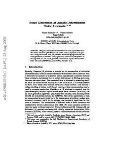
Deterministic Defect-Oriented Test Generation for Combinational Circuits1 Jaan Raik, Raimund Ubar Tallinn University of Technology, {jaan, raiub}@pld.ttu.ee Joachim Sudbrock Darmstadt University of Technology,
[email protected] Wieslaw Kuzmicz, Witold Pleskacz Warsaw University of Technology, {wbk, wap}@imio.pw.edu.pl Abstract A method is presented for deterministic test pattern generation using a uniform functional fault model for combinational circuits. The fault model allows to represent the physical defects in components and defects in the communication network of components by the same technique. Physical defects are modeled as parameters in generic Boolean differential equations. Solutions of these equations give the conditions at which defects are locally activated. The defect activation conditions are used as functional fault models for logic level test generation purposes. A method is proposed which allows to find the types of faults that may occur in a real circuit and to determine their probabilities. A defect-oriented deterministic test generation tool was developed, and the experimental data obtained by the tool for ISCAS’85 benchmarks are presented. It was shown that for the majority of cases 100% stuck-at fault tests do not cover 100% of the physical defects. The main feature of the new tool is that it allows to reach 100% coverage for the given set of defects or to prove the redundancy of not detected defects. Shorts are the dominant cause of faults in modern CMOS processes. In current approach the wired-AND fault model was considered.
1. Introduction Testing of VLSI circuits has faced a lot of problems produced by continuous emerging of new technologies and by growing complexity of circuits and systems. The most important question in testing today’s complex digital systems is: how to improve the testing quality at continuously increasing complexities of systems? Two main trends can be observed: defect-orientation and highlevel modelling. To follow the both trends, hierarchical approaches should be used. 1
Traditional very popular stuck-at fault (SAF) model has not withstood the test of time. It has been shown that high SAF coverage cannot quarantee high quality of testing, for example, for CMOS integrated circuits [1-3]. The reason is that the SAF model ignores the actual behaviour of digital circuits implemented as CMOS integrated circuits, and does not adequately represent the majority of real IC defects and failure mechanisms which often do not manifest themselves as SAF. The types of faults that can be observed in a real gate depend not only on the logic function of the gate, but also on its physical design. These facts are well known [2-5] but usually ignored in engineering practice. In earlier works on layout-based test generation techniques [4,5] the whole circuits were analysed as single blocks. Such an approach is computationally expensive and thus highly impractical as a method of generation of tests for real VLSI designs. In this work we characterise physical defects in library cells, determine their probabilities and then use this information for defect oriented test generation at the logic level. We verify the functionality of analysed gates or complex gates for all possible defects and find the actual functions performed, using either transistor-level simulation or analytical approach based on solving Boolean diffential equations. The defect characterisation process may be computationally expensive, but it is performed only once for every library cell. In other words, we replace in the cells the abstract logic fault models like SAF with realistic physical defect models. The defect lists of the library components embedded in the circuit are extended by additional physical defects in the close surrounding of the component to take into account also defects outside of components. For these defects additional characterization should be carried out by a similar way as for the library cells. In some cases the assumption can be made that the majority of defects occur inside the cells and not in the
The work was supported by EU projects IST 2000-30193 REASON, IST-2001-37592 eVIKINGS II, Estonian Science Foundation grants 5637, 5649, 5910, and by the Polish State Committee for Scientific Research project No. 4 T11B 023 24.
routing between them. Such assumption would not be realistic in the case of older CMOS technologies with two levels of metal and very dense routing. However, in stateof-the-art deep submicron technologies still only one or two levels are used inside cells but 6 or more levels of metal are available for routing. More routing levels means lower sensitivity to defects. Routing between the cells is less dense and various nodes are routed at various metal levels. As a result, probability of shorts outside cells is significantly reduced. In [6] a new approach was introduced for hierarchical defect simulation based on defect preanalysis for components, and using the results of preanalysis in higher level fault simulation. Here, we generalize this approach by introducing a functional fault model as a method for mapping faults from one hierarchical level to another. Based on this approach, hierarchical algorithm for defectoriented deterministic test generation is developed and implemented. The functional fault model in a form of a set of logical conditions (constraints) allows to represent the defects in components and in the communication networks by the same technique. Then we propose a methodology which allows to find the types of logic faults that may occur in a real circuit, to determine their probabilities of occurrence, and to find the input test patterns that detect these faults. We compare the results obtained in this way with the results of testing of the same circuits by the sequences of test patterns based on the conventional fault model. Experiments were carried out for the ISCAS’85 benchmark circuits. According to [10], shorts are the dominant cause of faults in modern CMOS processes. Due to the layout of cells in state-of-the-art technology, wired AND shorts are much more likely than wired OR shorts. Thus, in current approach the wired-AND fault model was considered. The paper is organized as follows. In Section 2 we present a new method of parametric fault modeling for carrying out defect analysis in digital circuits, and define the functional fault model as interface for mapping defects from transistor level to logic level. In Section 3 we show how the new fault model can be extended for representing defects with sequential behavior. Section 4 presents the results of a probabilistic analysis of defects by simulating them on the transistor level. In Section 5 we describe a new defect-oriented deterministic test generation algorithm. Section 6 presents experimental results, and finally, in Section 7 we draw the conclusions of this research.
2. Parametric defect modeling In this Section we present a new general fault model for describing and modeling arbitrary physical defects
first, in the components of a circuit and in the routing between the components. Consider a Boolean function y = f (x1, x2, …, xn) implemented by an embedded component C in a digital circuit. Introduce a Boolean variable d for representing a given defect in the component or in the surrounding of the component, which may affect the value y by converting the Boolean function f into another function y = f d (x1, x2, …, xn, xn+1, … xp). Here, in general case, the variables xn+1, … xp belong to the neighbourhood layout of the component which will influence the function y in the presence of defect d. Introduce now for the block C a generic parametric function
y* = f * ( x1 , x2 ,..., xn , xn+1 ,..., x p , d ) = d f ∨ df d (1) as a function of a defect variable d, which describes the behavior of the component simultaneously for the both, fault-free and faulty cases. For the faulty case, the value of d as a parameter is equal to 1, and for the fault-free case d = 0. The solutions of the Boolean differential equation
Wd =
∂y * =1 ∂d
(2)
describe the conditions which activate the defect d on a line y. The parametric modeling of a given defect d by equations (1) and (2) allows us to use the constraints (the solutions of Wd = 1) in defect-oriented test generation. To find Wd for a given defect d we have to create the corresponding logic expression for the faulty function fd either by logical reasoning or by carrying out directly defect simulation, or y by carrying out real x1 x4 experiments to learn the Short physical behavior of different defects. x2 For example, assume there is a short inside the transistor x5 x3 circuit in Fig. 1 described by the function y = x1 x2 x3 ∨ x4 x5 . Fig.1. Transistor circuit with a short
The short changes the function of the circuit as follows: y d = ( x1 ∨ x 4 )( x 2 x3 ∨ x5 ) .
Using the defect variable d for the short, we create a generic Boolean differential equation and solve it as follows:
∂y * ∂ (( x1 x2 x3 ∨ x4 x5 )d ∨ ( x1 ∨ x4 )( x2 x3 ∨ x5 )d ) = = ∂d ∂d
= x1 x2 x4 x5 ∨ x1 x3 x4 x5 ∨ x1 x2 x3 x4 x5 = 1
From the equation three possible solutions follow: T = {10x01, 1x001, 01110}. Each of them can be used as a test pattern for the given short. On this contra-example, it is easy to show the inadequacy of the stuck-at fault (SAF) model for testing the transistor level faults. For example, the set of five test patterns 1110x, 0xx11, 01101, 10110, 11010 which test all the stuck-at faults in the circuit does not include any of the possible test solutions from the set T for detecting the short. Component
Wd
describes the conditions (constraints) which activate the fault d on a line y. The apostrophe at y means that the value of y belongs to the previous clock cycle. The condition
W d = x1 x2 x3 y ' = 1 means that we need for
testing of the short a sequence of two patterns. First, we have to set the value y = 0 (for example, by assigning x3 = 0), then we have to apply the pattern x1 = 1, x2 = 1, x3 =1. Bridging fault causes a feedback loop:
y
F(x1,x2,…,xn)
W d = ∂y * / ∂d = x1 x2 x3 y ' = 1
Activated by W d path
x1
Defect
&
x2
x3
Fig. 2. Functional fault model for a physical defect The described method represents a general approach to map an arbitrary physical defect onto a higher (in this case, logic) level. A physical defect in a component can be represented by a logical constraint Wd = 1 to be fulfilled for activating the defect to the output of the component (Fig.2). The event of erroneous value on the output y of a functional component can be regarded as a SAF taking place at the logical constraint Wd = 1. Table 1. Activating conditions for different defects No 1 2 3 4
Defect SAF xk ≡ 0 SAF xk ≡ 1 Short between xk and xl Exchange of lines xk and xl
5
Delay fault on the line xk
r
Conditions W xk = 1 xk = 0 xk = 1, xl = 0 xk = 1, xl = 0, or xk = 0, xl = 1 xk = 1, x’k = 0, or xk = 0, x’k = 1
Some examples of the conditions Wd for different type of defects (where SAF is a particular extreme case) are given in Table 1 (here xk is the observable variable, and x’k is the variable at the previous time moment).
3. Sequential physical defects Consider a short between two lines xk and xl in the circuit in Fig. 3, which creates a feedback loop. The generic parametric function for describing the behavior of the circuit simultaneously for both, fault-free and faulty cases has the following form:
y* = d ( x1 x2 ∨ x3 ) ∨ d ( x1 x2 y ∨ x3 ) = = x1 x2 (d ∨ y ' ) x3 The solution of the Boolean differential equation
y
&
Equivalent faulty circuit:
x1 x2
&
&
&
y
x3
Fig. 3. Bridging fault with feedback loop
From this example we see that in the general case the constraints for activating a fault may be spread over different time steps, and represent sequences of patterns. We see also that the method for describing faults by generic Boolean differential equations allows us directly to attack the problem of testing so called ”sequential faults” which convert combinational circuits into sequential ones, or which increase the number of states in sequential circuits. Test generators which are able to work with such faults are missing.
4. Probabilistic defect modeling In the following we consider one kind of physical defects in CMOS gates - shorts between conducting regions. This is one of the most important sources of faults in CMOS digital circuits. However, the methodology can be extended to other types of physical defects as well (e.g. breaks, opens etc.). A short is a piece of extra conducting material that connects a pair of separate conducting regions in the integrated circuit. This affects the connectivity of the circuit - two separate electrical nodes become connected. It is intuitively obvious that probabilities of shorts depend on the layout of the circuit. Conducting regions that are adjacent to one another are more susceptible to shorts than regions that are separated by a large distance. We assume that every defect that results in a short can be
approximated by a circle. To estimate the probabilities of shorts between pairs of nodes we use the concept of critical area for shorts [3]. The critical region for shorts is such a region in the circuit that if the center of a defect of a given radius R is located anywhere inside the critical region, a short between two adjacent conducting regions occurs. The critical area is the area of the critical region. It depends on the shapes and locations of the conducting regions that can be shorted and is a function of the defect radius R. The radii of defects are random and can be characterised by a probability density function Pdf(R). We assume that the probability of a short between a pair of conducting regions that correspond to a pair of electrical nodes is proportional to the critical area for these two regions. The critical area for shorts is a function Ps(R) of the defect radius R. Since the defect radii exhibit a random distribution, the product Pdf(R) * Ps(R) integrated over the range of R where Ps(R) > 0 can be taken as the measure of the total probability of shorts between a given pair of nodes. Pt = ∫ Ps(R) Pdf(R) dR The first step in identification of logic faults and their probabilities is to calculate Pt for all pairs of conducting regions representing electrical nodes. If for a given pair Pt = 0, this pair of nodes cannot be shorted and is not taken into account. For the pairs that can be shorted the logic faults are determined. To carry out the characterization of the defects we used SPICE for simulating purposes. The shorts were represented by resistors. We tried several resistance values in the range from 0.01 ohm to 200 ohm. The gate behaviour at the logic level did not depend on this resistance. The waveforms obtained from the simulation allow to determine the actual logic function performed by the faulty circuit. In this way the functional faults that result from shorts are identified and their probabilities are determined. This procedure and the software developed for this purpose are described in more detail elsewhere [7]. Methodology which allows to obtain the defect tables was described in [8].
5. Deterministic test generation algorithm In order to automatically generate test patterns for defects in CMOS technology, a new deterministic algorithm (Fig. 4) was developed and implemented. It is based on a generalization of the PODEM algorithm [9]. In the following, the main steps of the new method are explained. Initial objective. In the PODEM algorithm for stuckat faults, excitation of the fault to be tested is the primary objective. This is carried out by finding a suitable assignment to primary inputs (PI) belonging to the cone of the fault location in a way that the fault would be
activated. However, in order to target specific defects inside a gate every gate input (GI) must have some certain value to cover the fault. The main difference to the traditional PODEM algorithm is therefore, that the initial objective does not consist of a value assignment to a single line, but of several objectives. GI vector reordering. In a general case, several GI vectors in a defect table for a gate can detect the same fault. Thus, the following defect coverage based heuristics was implemented to rearrange the order of GI vectors for which to generate tests. At the point in the algorithm, where we have to select the next GI vector to be targeted, calculation of the number of undetected faults within the faulty gate is carried out. GI vector with the highest number of uncovered faults will be chosen. This heuristics is aimed at minimizing the number of deterministic tests to be generated by maximizing the fault coverage of each test. GI vector’s defect coverage computation can also be done by summing up the probabilities of each fault being tested by each GI vector. It will become especially useful, if a 100 % test coverage is not the main goal, but a limited number of test vectors while achieving a high probabilistic test efficiency. Backtrace and backtrack. To fulfill the test generation objectives in fault activation and propagation, a so called backtracing process is applied. During backtrace, values are recursively assigned to preceding circuit lines along a single path until a primary input (PI) is reached. The desired value is assigned to the PI and the circuit is simulated with the set of current value assignments. If the simulation gives inconsistent values to GI lines of the faulty gate then a backtrack is performed: the last PI assignment is inverted and circuit is simulated again. Otherwise, the next objective will be backtraced. The algorithm includes two types of objectives to backtrace. The first one is the initial objective explained above. The latter is the objective to propagate fault-effect D from the D-frontier towards the primary outputs (PO). Fault effect propagation. When the initial objective has been satisfied by the backtrace process, the next step will be to propagate the fault from the faulty gate output to at least one of the primary outputs. To propagate the fault, further backtracing steps have eventually to be performed, each time followed again by a simulation. The possibility to propagate the fault from the D-frontier to at least one primary output with the current PI assignment has to be checked continuously by a process called X-path check. This procedure finds out whether there exists a signal path from the line with a fault effect (D) to some PO such that all the line values along the path hold don’t-care (X) values. If X-path check fails for all the lines in the Dfrontier then the PI assignment will be backtracked. The defect can be regarded as detected, if the fault is propagated to one or more primary outputs.
Fig.4. Defect-oriented test generation algorithm
7. Experimental results Tables 2 and 3 present the experiments carried out for detecting the AND-short defects in a 0.8 µm CMOS technology. We used circuits resynthesized from the verilog versions of the ISCAS85 suite as benchmarks for tests. The circuits were synthesized by SYNOPSYS Design Compiler. Two versions of each circuit was synthesized. Circuits with extension ‘cmp’ were created by a Design Compiler script that used the complex gates plus 2-input NOR and an inverter as the library basis. Circuits with extension ‘all’ are synthesized from a library containing all the gates for which defect tables were created. Table 2 gives the results of the deterministic defectoriented ATPG implementing the algorithm presented in the previous Section. Column 2 shows the total number of defects in the fault tables summed over all the gates belonging to the netlist. Column 3 reflects the number of gate redundant defects. These are defects that cannot be covered by any input vector of the gate. For example, AND-short between the two inputs of the AND gate is a gate redundant fault. In column 4, circuit redundant defects are counted. Circuit redundant defects are defects that cannot be tested because the circuit structure doesn’t allow to generate a test for any of the GI vectors covering the defect. Column 5 shows the number of defects covered by the tests. Column 6 gives the umber of aborted defects, which are the defects that were not covered but that were not proved redundant.
Then, three fault coverages, both by enumerating the ratio of detected defects and calculating the defect probabilities are provided. The first coverage shows the ratio of detected defects versus the total set of defects. In the second column, gate redundancy has been excluded. The third coverage measure shows the defect efficiency, or test coverage. In this value, both, gate redundancy and circuit redundancy has been subtracted. Note, that the probabilistic coverage should be considered since it takes into account the probabilities of occurrence of different defects. Table 3 shows the simulated defect coverage of a SSA tests generated. The tests covered 100 % of SSA faults in the benchmark circuits. The experiments prove that relying on 100 % SSA test coverage would not necessarily guarantee a good coverage of physical defects. Although in nearly 50 % on the tested cases, SSA-based ATPG was able to cover all the detectable defects, for most of the circuits the defect-oriented tool yielded better results. For example, for c2670_cmp the defect-coverage obtained by the SAF tests was 1.6 % lower than the result of the proposed tool. An interesting remark is that up to 25 % (see c880_all!) are proved redundant by the new tool. Thus, a very large portion of CMOS defects cannot be tested by any voltage test at all. The minimization of the number of generated test vectors was not the goal of current research. However, the test lengths achieved by the proposed method were roughly in the same order as the ones for SSA tests.
8. Conclusions A new deterministic defect-oriented test generation method has been developed and implemented as a tool. In this method, we use a new functional fault model for mapping physical defects from transistor level to logic level. The model allows the first time to formalize test generation in a straightforward manner for detecting the defects that transform a combinational circuit into a sequential one. In the method, the conditional probabilities of defects can be also used for probabilistic defect coverage calculation. A probabilistic analysis of CMOS physical defects in the library cells has been carried out to create for each library cell a defect table. Based on these data, and by using the implemented tool it was possible to generate deterministic test patterns to reach 100% physical defect coverage or to prove the redundancy of physical defects.
Table 2. Experimental results of the defect-oriented deterministic ATPG Enumerative
Table 3. Defect coverage of SSA-tests generated by a standard deterministic ATPG Enumerative
93,70 83,81 94,58 89,82 92,16 85,88 93,38 90,46 98,66 79,56 86,44 75,34 85,27 80,63 79,69 80,26 82,39 77,02
100 100 99,93 99,10 97,03 98,71 98,02 97,80 99,90 100 96,57 99,83 99,46 99,49 98,54 98,73 97,53 99,81
100 100 100 100 100 99,95 100 100 100 100 100 100 100 100 100 99,97 100 100
# test patterns
100 100 100 100 100 99,95 100 100 100 100 100 100 100 100 100 99,97 100 100
defect efficiency (test coverage),%
100 100 99,94 99,21 97,59 99,04 98,46 98,32 99,92 100 97,11 99,83 99,53 99,61 98,87 98,86 98,04 99,80
defect coverage (- gate red.), %
88,33 88,55 89,41 89,59 88,20 88,45 88,60 89,25 88,55 85,12 87,85 85,09 87,50 86,91 87,45 86,15 87,79 83,44
defect coverage, %
0 0 0 0 0 3 0 0 0 0 0 0 0 0 0 2 0 0
Probabilistic
defect efficiency (test coverage),%
1703 4105 3547 4802 3041 5967 8014 14311 23904 1293 3898 2876 4639 2789 5326 6599 12988 20387
defect coverage (- gate red.), %
0 0 2 38 75 55 125 244 19 0 116 5 22 11 61 74 260 41
defect coverage, %
225 531 418 520 332 721 906 1479 3071 226 423 499 641 409 703 985 1546 4005
# aborted defects
# cct. redundant defects
1928 4636 3967 5360 3448 6746 9045 16034 26994 1519 4437 3380 5302 3209 6090 7660 14794 24433
# covered defects
# gate redundant defects
C432_cmp C499_cmp C880_cmp C1355_cmp C1908_cmp C2670_cmp C3540_cmp C5315_cmp C6288_cmp C432_all C499_all C880_all C1355_all C1908_all C2670_all C3540_all C5315_all C6288_all
# of defects
circuit
44 80 38 83 38 102 126 76 43 74 79 56 87 38 107 118 83 36
References
Probabilistic
circuit
# of defects
# gate redundant defects
# covered defects
defect coverage, %
defect coverage (- gate red.), %
defect efficiency (test coverage),%
defect coverage, %
defect coverage (- gate red.), %
defect efficiency (test coverage),%
# test patterns
C432_cmp C499_cmp C880_cmp C1355_cmp C1908_cmp C2670_cmp C3540_cmp C5315_cmp C6288_cmp C432_all C499_all C880_all C1355_all C1908_all C2670_all C3540_all C5315_all C6288_all
1928 4636 3967 5360 3448 6746 9045 16034 26994 1519 4437 3380 5302 3209 6090 7660 14794 24433
225 531 418 520 332 721 906 1479 3071 226 423 499 641 409 703 985 1546 4005
1694 4105 3545 4802 3041 5967 8010 14307 23904 1284 3898 2874 4639 2789 5299 6594 12988 20387
87,86 88,55 89,31 89,59 88,17 88,13 88,49 89,22 88,55 84,13 87,85 84,85 87,50 86,91 86,95 85,95 87,79 83,44
99,47 100 99,83 99,21 97,56 98,67 98,34 98,28 99,92 98,84 97,11 99,55 99,53 99,61 98,29 98,64 98,04 99,80
99,47 100 99,89 100 99,97 99,58 99,88 99,96 100 98,84 100 99,72 100 100 99,42 99,74 100 100
93,18 83,81 94,41 89,82 92,16 85,46 93,19 90,39 98,66 78,61 86,44 75,00 85,27 80,63 79,13 80,05 82,39 77,02
99,48 100 99,77 99,10 97,03 98,29 97,84 97,73 99,90 99,05 96,57 99,50 99,46 99,49 97,97 98,52 97,53 99,81
99,48 100 99,84 100 99,99 98,29 99,81 99,93 100 99,05 100 99,66 100 100 99,44 99,76 100 100
50 80 47 85 43 110 127 97 43 54 79 39 87 41 110 131 90 36
[1] J.M. Soden, C.F. Hawkins. Quality Testing Requires Quality Thinking. Proc. ITC, 1993,pp. 596. [2] W.Maly, et al. System Characterization of Physical Defects for Fault Analysis of MOS IC Cells. Proc. 1984 ITC, pp. 390-399, 1984. [3] J.P.Shen, et al.. Inductive Fault Analysis of MOS ICs. IEEE Design&Test, pp.13-26, 1985. [4] P.Nigh and W.Maly. Layout - Driven Test Generation. Proc.1989 ICCAD, pp. 154-157, 1989. [5] M.Jacomet, W.Guggenbuhl. Layout-Dependent Fault Analysis and Test Synthesis for CMOS Circuits. IEEE Trans. on CAD, vol. 12, pp. 888-899, 1993. [6] R.Ubar, W.Kuzmicz, W.Pleskacz, J.Raik. DefectOriented Fault Simulation and Test Generation in Digital Circuits. Proc. ISQED, 2001, pp.365-371. [7] M.Blyzniuk, W.Pleskacz, M.Lobur, W.Kuzmicz Estim. of Probability of Different Functional Faults Caused by Spot Defects in VLSI Circuits. Proc. TCSET 2000 Conf., Slavsko, Ukraine, 2000. [8] W. A. Pleskacz, et al.. CMOS Standard Cells Characterization for Defect Based Testing. Proc. of the Int. Symposium on Defect and Fault Tolerance in VLSI Systems, pp. 384-392, Oct. 2001. [9] P.Goel. An Implicit Enumeration Algorithm to Generate Tests …. IEEE Trans. on Comp., vol. C-30, no.3 pp. 215-222, Mar. 1981. [10] M Sachdev. Defect Oriented Testing for CMOS Analog and Digital Circuits. Kluwer Academic Publisher, 1998.