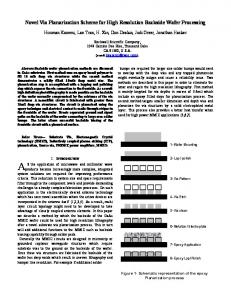
Development of Backside Process for Alternative Die Attach on HBT Jason Fender*, Terry Daly*, Darrell Hill**, Lakshmi Ramanathan**, Philip Bowles**, Neil Tracht** Freescale Semiconductor, Inc. Tempe Fab*, WPSL**, 2100 E. Elliot Road, Tempe, AZ, 85284
[email protected];
[email protected];
[email protected];
[email protected];
[email protected];
[email protected]
Keywords: Backside, Metallization, Solder, Die Attach Abstract To meet the need for a wire bond-free solution for power amplifier HBT die, a backside process has been developed. Solderable contacts are formed on the backside of the die under the constraints of working with a thinned, mounted GaAs wafer. Backside process steps are described in this paper and preliminary assembly results are provided. INTRODUCTION Market demand places relentless pressure on reducing both the size and cost of modules for wireless handsets. The size of the module can be significantly reduced (and potentially the cost as well) if bond wires are eliminated in favor of flip-chip techniques. This method involves forming solderable bumps on the front side of the wafer. Unfortunately, flip-chip does not work well for power amplifier die, which have high power dissipation densities on the order of 5-10 W/mm2. In order to achieve low thermal resistance while flipped, there must be a direct, allmetal path to the heat sink. This all metal path induces mechanical stresses from CTE mismatch directly on the transistor active area, jeopardizing device reliability. Since it is generally not practical to flip-chip all but one die in a multi-die product, a need exists for a wire bond-free solution for power amplifier die. This paper presents an alternative solution to meet that need. PROCESS REQUIREMENTS One promising approach to create a wire bond-free solution is to form electrical contacts on the back of the die. Though-wafer vias can then used to connect to the devices on the front side of the die (Fig. 1).
This type of approach has been reported for over 10 years, however, it has not been practical due to incompatibility between die metallization and the solder types for die attach. The backside metal is generally gold (Au) and is readily consumed by tin (Sn)-containing solders, degrading or destroying interconnect metallization. Also, many solders are embrittled when alloyed with Au, reducing their thermal cycling reliability. The drive toward lead-free products exacerbates these issues by placing additional restrictions on the solder types which may be used. Due to this limitation, a key component of the solution is inclusion of a solderwettable barrier within the patterned backside metallization. This allows the solder to adhere to the die connection without consuming the Au metallization. A further requirement is a non-solder-wettable barrier. This barrier is necessary if the metal under the solderwettable barrier is wettable, as is the case of Au. The solder contacts on the substrate can be larger or shaped differently compared to the solderable contacts on the wafer, exposing the Au metal on die to the solder on the substrate when assembled. Without the non-wettable barrier, the solder can attack the interconnect metal and even be drawn into the through-wafer vias from the edges of the structure. In addition to the difficulty of forming electrical contacts on the backside, the condition of the wafer introduces additional constraints. All processing is done on thinned wafers mounted on sapphire carriers. Also, the processing must be compatible with the through-wafer vias. Photo steps must be capable of filling the vias, and film depositions must provide adequate step coverage. Finally, the processing temperature must be controlled below the softening or melting point of the mount material to prevent the wafer from detaching from its carrier. PROCESSING STEPS
Transistor Die
Solder Substrate for die attach
Figure 1: Diagram of Backside Die Attach
The backside process flow begins with a completed device on a full thickness wafer. As is typical with backside via processing, the wafers are mounted to a sapphire or other carrier compatible with backside processing. The wafer is then thinned to device requirements. A photoresist pattern and dry etch is used to attach vias to the front side of the wafer. Sputter deposited titanium (Ti) and Au stack is used as the seed for electroplating a thick Au layer. At this point
CS MANTECH Conference, May 14-17, 2007, Austin, Texas, USA
159
in the flow, the process steps described have been typical for an epoxy attach, wire bonded die. The following steps are unique to the alternative die attach devices. A photoresist pattern is used to electroplate solderable metal, such as nickel (Ni), using the thick plated Au as the seed layer. The thickness of this metal must be sufficient to sustain multiple reflows without being consumed by the solder. The photoresist is then removed. A photoresist pattern and etches are then used to separate the blanket Ti/Au into individual backside features. The photoresist must again be removed. Mention is made to each of these photoresist removal steps because of their effect on the mount material. Care must be taken to prevent the mount material from being overheated or dissolved. The non-wettable solder barrier is then deposited over the surface of the wafer. This barrier can be any type of dielectric, deposited or spun-on. The key is, again, processing within the limitations of the mount material. A PECVD SiN film was used in this embodiment. Openings in the dielectric are then formed with a photoresist pattern, etch, and resist removal. The solder barrier metal (Ni in this embodiment) is not wettable in this state because of oxidation, so the oxidation must be removed and a wettable layer deposited on top. A sputter etch is done prior to using sputtered Au as the wettable layer. The sputtered Au is then removed everywhere except on top of the solder barrier features by photo patterning and etching. The wafer is then debonded from its carrier and processed through die singulation. The process steps are shown in Figure 2. Using multiple short flows with the process, layout design rules were also established. Layout is a critical component and is based on process and assembly capabilities.
Sapphire substrate
Sapphire substrate
Sapphire substrate
Sapphire substrate
Normal thickness HBT PA wafer
Sapphire substrate Normal thickness HBT2 PA wafer Sapphire substrate
Sapphire substrate Thin wafer Sapphire substrate
160
CS MANTECH Conference, May 14-17, 2007, Austin, Texas, USA
Ni barrier GaAs die
Solder cladding
Substrate
Sapphire substrate
Figure 2: Representative process steps for wire bond-free die attach
RESULTS Wafers were produced with the described backside process, also referred to as the direct die attach process (Fig. 3).
Sapphire substrate
Sapphire substrate Figure 2: Optical photo of backside of a processed die using direct die attach
Sapphire substrate
To test the ability of the solder barriers, both wettable and non-wettable, solder reflow reliability tests were performed. Excessive amounts of solder were deposited on the die and the die were put through multiple reflow cycles. Microscope imaging was used to examine cross sections of the bonds (Fig. 3). Daisy chain structures have also been assembled and reliability tested with passing results.
SOLDER NonWettable Barrier
Wettable Barrier
DIE Figure 3: Microscope photo of die processed through multiple reflow cycles
CS MANTECH Conference, May 14-17, 2007, Austin, Texas, USA
161
CONCLUSIONS An alternative die attach process has been shown to be feasible using the steps reported here. Multiple samples have been produced and processed through reliability and RF testing with acceptable results. The direct die attach process provides a viable wire bond-free solution. ACKNOWLEDGEMENTS The authors would like to thank process engineering, associates and technicians who assisted in running the samples, specifically G. Hernandez for the photo processing and F. Clayton for dry etch processing. Additionally, the authors thank J. Jang for the reflow tests and analysis. REFERENCES [1] Peter H. Ladbrooke, MMIC Design GaAs FETs and HEMTs, Ch. 3: Overview of Passive Elements, p. 29, 1989 [2] Sakai et al., A New Millimeter-Wave Flip-Chip IC on Si Substrate, 1994 Asia-Pacific Microwave Conference Proceedings, pp. 291-294, 1994 [3] Daly T., Fender J., Duffin B., Kottke M., Optimization of Metal Adhesion for GaAs Backside Wafer Processing, 2003 GaAs Mantech Technical Digest, 2003
ACRONYMS HBT: Heterojunction Bipolar Transistor CTE: Coefficient of Thermal Expansion PECVD: Plasma Enhanced Chemical Vapor Deposition SiN: Silicon Nitride
162
CS MANTECH Conference, May 14-17, 2007, Austin, Texas, USA