Copy of: Proceedings IEEE 2007 Int. Conference on Microelectronic Test Structures, Vol. 20, March 2007
Device Array Scribe Characterization Vehicle Test Chip for Ultra Fast Product Wafer Variability Monitoring Christopher Hess, Sharad Saxena1, Hossein Karbasi2, Senthil Subramanian2 Michele Quarantelli3, Angelo Rossoni3, Stefano Tonello3, Sa Zhao, Dustin Slisher4 PDF Solutions Inc., San Jose, CA 95110, USA Phone: +1-408-938-6436, FAX: +1-408-280-7915, Email:
[email protected] 1 PDF Solutions Inc., Richardson, TX 75082, USA 2 PDF Solutions Inc., San Diego, CA 92128, USA 3 PDF Solutions Inc., 25015 Desenzano, Italy 4 IBM Microelectronics, East Fishkill, USA
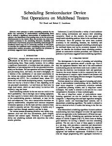
2 Test Chip Design A novel transistor array architecture is introduced to achieve maximum area efficiency and simplicity in addressing a device under test as well as supporting parallel testing. 2.1 Maximizing Area Efficiency The proposed device array will pack 32 devices within an array, where all routing just requires two metal layers. Thus, the array can be placed underneath the pads, which are implemented in Metal 3 and above. The left side of Figure 1 illustrated this approach. y
Vdd/Gnd & selection signals, to next array
GS
28 29 30 31 24 25 26 27
1 Introduction For 65nm technologies and below, it is required to characterize much larger device sample sizes. There is a stronger impact of layout pattern on device performance due to strong OPC and focus and exposure variability. 300mm wafers show more significant spatial trends than in previously technology nodes. It is simply impossible to characterize all those effects by just looking at a few devices on 5, 9 or 15 dies per wafer. Device arrays have been introduced to improve area usage and allow larger design of experiments (DOE). [LeJa03], [ScLT00], [SMCS04], [ScEi05] describe just a few of those. However, even if the number of devices per die can be increased, test time is the ultimate bottleneck in collecting the required data from much larger sample sizes. Lately, analog measurement systems are being introduced that provide significantly higher number of parallel measurement channels. However, none of the existing device array architectures truly support massive parallel testing. Thus, we are introducing a comprehensive wafer level variability monitoring system, which will enable high volume sampling within given area and test time budget.
20 21 22 23
S
4 Multi-layer pads stacked over an 8x4 DUT array
16 17 18 19 12 13 14 15
D
8
9
4
5
10 11 6
7
0
1
2
3
local Row decoder
Abstract – Lower supply voltages and aggressive OPC on 65nm and below technologies are causing larger variability of critical device parameters like Vt and Id. With ever increasing clock frequencies, more and more performance related yield loss can be observed even for purely digital circuits. To design more robust circuits it is required to characterize device variability within die, within wafer, wafer to wafer as well as lot to lot. Large samples of device measurements are necessary for accurate variability characterization. A novel Characterization Vehicle (CV) has been developed, which achieves an extremely efficient placement of several hundred devices by arranging them underneath the probing pads. Placed next to product chips, those Scribe CV test chips are providing Vtlin, Idlin, Vtsat, Idsat, Gmlin, and Gmsat for more than 25000 devices per 300 mm wafer requiring less than 20 minutes for testing.
GF Vdd/Gnd & selection signals from previous array, and global selection logic
z
Global Column decoder x A[0:1]
A[2:4]
Figure 1: Concept of arranging 32 devices (right) under probe pads (left).
2.2 Simplicity in Addressing a Device Under Test The proposed array has 32 devices under test (DUT), which share the source and drain pins. There are no selection devices in the source and drain path, which is important to gain accurate measurements. Furthermore, it eliminates the risk of back-biasing wells, which can easily happen, if a selection device is implemented along the pad to source path. Smart and balanced routing limits the
Copy of: Proceedings IEEE 2007 Int. Conference on Microelectronic Test Structures, Vol. 20, March 2007
resistance between each pad and the source or drain pins of each DUT to 5 ohms. In the device array presented here, the only selection device is being used in the pad to gate path to turn on a specific DUT. For the gate pin, a force and sense path is being used to monitor and adjust the gate voltage if required. The selection logic is purely combinatorial as indicated at Figure 2 and it is being shared among several arrays. The absence of timing critical circuitry reduces design time, simplifies testing and ensures a very robust design among a variety of technologies. Gate
Force
Sense
S
dScribe CV Test chips are being implemented within the scribe line of product wafers. A layout example can be seen in Figure 4. The center section is shown on the left. The center 8 pads are used for power supply and address bits driving the common logic for 10 arrays each holding 32 devices. Each array is placed under 4 pads as can be seen in the center of Figure 4. The right side shows the placement of 8 devices under one single pad.
D
Row decoder
Gate
3 Experimental Results
Total of 8 rows
Figure 2: Schematic of one array the Device Scribe CV test chip.
2.3 Support of Parallel Testing As shown in Figure 3 on the right, 10 such arrays are implemented in one pad group to be tested in parallel. The Device Scribe CV® Test Chip or simply dScribe CV can then be placed in one or more locations on a reticle next to product chips as shown on the left side of Figure 3.
5 NMOS 8x4 DUT arrays
Global logic
5 NMOS 8x4 DUT arrays
Figure 3: Packing of arrays into one Scribe CV Test Chip (right) and potential placement on a multi product reticle (left).
Figure 4: Zoom in from left to right within a layout example of a Device Scribe CV Test Chip.
3.1 High Speed Testing using pdFasTest II In general, testing can be executed as early as the first metal layer with pads has been manufactured. Dependent on the ILD thickness and softness it is recommended to start testing one or two metal layers higher to ensure robust test results if probing related stress shows an impact. The pdFasTestII® test system is being used to test the dScribe CV Test chip. It provides up to 72 parallel analog testing channels. The 10 arrays of the dScribe CV are being tested in parallel. Within each array, the 32 devices are tested in sequence. pdFasTestII just needs 11 seconds to obtain two I/V curves for each of the 320 devices, one for linear region and one for saturation region. From those curves, the tester derives key device parameters like Vtlin, Idlin, Vtsat, Idsat, Gmlin, and Gmsat. A regular parametric tester needs for the same task 11 minutes, which translates into a test speed gain of 60. Despite the large speed advantage, correlation of test results is excellent as can be seen in Figure 5 and Figure 6.
Copy of: Proceedings IEEE 2007 Int. Conference on Microelectronic Test Structures, Vol. 20, March 2007
3.00e-5
0.001
2.00e-5
0.0005
1.00e-5
0 -0.0015
-0.001
-0.0005
Individual Transistor (arb. Units)
IdSat (Parametric Tester)
0.0015
0
0.0005
0.001
0.0015
-0.0005
0.00e0
-0.001
-1.00e-5
-0.0015
-2.00e-5
IdSat (pdFasTest II)
Figure 5: Comparison of Id measurements taken with pdFasTest II and a standard parametric test system.
-3.00e-5
-3.00e-5
-2.00e-5
-1.00e-5
0.00e0
1.00e-5
2.00e-5
Transistor Array (arb. Units)
3.00e-5
Figure 7: Comparison of Id data from identical transistor layouts taken either from a device array or devices connected straight to the pads.
0.35
VtSat (Parametric Tester)
0.25 0.15
3.3 Applications
0.05 -0.35
-0.25
-0.15
-0.05 -0.05
0.05
0.15
0.25
0.35
-0.15 -0.25 -0.35
VtSat (pdFasTest II)
Figure 6: Comparison of Vt measurements taken with pdFasTest II and a standard parametric test system.
3.2 Data Accuracy To evaluate the accuracy of data taken from a device array as suggested in this paper, we have implemented identical transistor layouts on a FEOL CV twice, once connected within the device array and once connected straight to individual pads. Direct comparison between the individually padded transistors and the arrays is difficult, because they are on different locations of the wafer and across chip variation between the two locations creates a difference between the two sites. The correlation between the arrays and individually padded devices is evaluated by comparing the distributions of the two sets of measurements by means of a probability-probability (P-P) plot. Figure 7 is an example P-P plot for Idsat, showing good agreement of the device array and individually padded transistor distribution. Thus, using pdFasTest II to measure the proposed device array is a very powerful solution to increase sample size by simultaneously decreasing test time.
The dScribe CV Test chip in conjunction with the pdFasTestII fast parallel testing provides a very large sample of transistor measurements with minimal test time. It enables the testing of more than 300 transistors on all wafers and all die on a 300 mm wafer. This volume of data enables many applications that are not feasible with limited parametric data available from standard process control monitor (PCM) testing, typically 9-15 die on a wafer. The effectiveness of combination of transistor arrays and pdFasTestII® testing was evaluated by comparing the transistor measurements obtained from a dScribe CV with conventional individually padded process-control monitor (PCM) structures. Figure 8 shows a typical Vth-Idrive comparison. The dScribe CV measurements are in good agreement with the PCM measurements from a typical parametric tester. In addition, the much larger sample of data available from dScribe CV, provides a better estimate of transistor performance variability than available from PCM measurements typically taken on the same wafers. The much larger measurement sample size available from dScribe CV also allows a better decomposition of the transistor performance variation into within wafer spatial components and other sources of variation like wafer-towafer and lot-to-lot variation. For example, Figure 9 shows examples of spatial patterns we have observed in dScribe CV measurements from production wafers that contribute to across-wafer non-uniformity. Such detailed characterization of across-wafer non-uniformity is not possible with typical PCM sampling plans.
Copy of: Proceedings IEEE 2007 Int. Conference on Microelectronic Test Structures, Vol. 20, March 2007
IdSat (arb units)
X: dScribe +: PCM
1265
1216
1391
1123
1135
1051
1239
1141
1171
1122
1106
0.657
1081
1103
1032
1255
1038
1039
1111
2.568
2.742
2.047
2.221
1169
1107
1074
1001
948.5
1018
0.785
2.221
2.221
2.047
-1.299
1.525
2.394
1086
1083
1100
1021
942.7
2.568
2.568
2.742
3.089
2.394
2.568
2.394
1.699
1166
1060
997.3
-0.604
0.959
2.221
-1.82
-0.778
3.263
-1.126
-0.257
-1.82
1021
1061
-0.778
2.221
1.352
1.525
2.394
2.047
1.178
2.047
2.047
-1.473
-1.126
3.263
-0.604
-1.126
0.0904
-0.257
0.264
-0.952
-1.299
-1.299
-0.604
623
633.6
653.2
685
680.5
NMOS
VtSat (arb units) 595
641
578.7
639.8
579.1
630.6
628
621.6
0.0752
572.1
539.3
599.5
589.3
580.3
586.2
582.9
0.77
1.117
0.0752
1.014
552.1
518.7
567.1
593.3
566.7
607
0.145
0.249
2.057
0.145
1.188
0.596
0.944
553.9
543.9
614.4
510.7
593.9
0.84
2.16
0.77
2.578
0.423
1.536
-0.272
1.117
523.3
623.4
561.9
-0.0986 0.77
-0.0284 1.883
0.667
0.145
-0.446
0.423
-0.446
502.1
527.3
0.667
1.014
0.145
0.84
0.944
1.188
-0.376
0.944
0.423
-0.446
0.596
0.249
0.249
0.84
0.667
1.465
1.117
0.249
0.77
0.249
-0.793
Figure 8: Comparison of dScribe CV measurements with standard PCM measurements from a parametric tester.
PMOS
Figure 10: Spatial pattern observed on a set of excursion wafers with a large number of non-functioning devices (NMOS left; PMOS right).
2500 1500 500 0
Figure 9: Spatial patterns of device performance revealed by full wafer sampling.
Further applications of the dScribe CV include: detailed spatial analysis of across wafer non-uniformity of transistor performance, correlation of transistor performance to product yield to quantify and understand transistor related yield loss, excursion monitoring, automated signature analysis of spatial patterns. Moreover, in conjunction with additional inline data and equipment logs this data can be used to find equipment level root causes for excursions. For example, Figure 10 shows the spatial pattern observed on a set of excursion wafers with a large number of non-functioning devices. Examination of the spatial pattern of the failing devices helps identify root causes of such excursions. Figure 11 shows the distribution circuit delay figure of merit (FoM) obtained from a large sample of dScribe CV based measurements. The large population provides a more accurate estimate of the delay distribution than would be possible with typical PCM measurements. For example, the slow tail, which would result in slow parts, can be seen in the dScribe CV measurements and is not apparent with a much reduced sampling.
Product Delay Figure of Merit Figure 11: Large sample size of device measurements allows estimation of tails in the performance distribution.
4 Conclusion Compared to conventional single padded devices placed in a scribe line, the Device Scribe Characterization Vehicle Test Chip based monitoring system provides more than 1000 times more data by maintaining the same area (32x gain) and test time (60x gain) budget. It is a very fast, robust and comprehensive system to characterize device variability. The dScribe CV is placed next to product chips. Parallel testing using pdFasTest II provides Vtlin, Idlin, Vtsat, Idsat, Gmlin, and Gmsat for more than 25000 devices per 300 mm wafer in less than 20 minutes without compromising data accuracy. The dramatically increased sample size enables detailed correlation of transistor performance to product yield data to better understand transistor related yield loss including excursion monitoring and automated signature analysis of spatial patterns.
Copy of: Proceedings IEEE 2007 Int. Conference on Microelectronic Test Structures, Vol. 20, March 2007
References [LeJa03]
[ScLT00]
R. Lefferts, C. Jakubiec; "An Integrated Test Chip for the Complete Characterization and Monitoring of a 0.25gm CMOS Technology that fits into Five Scribe Line Structures", IEEE International Conference on Microelectronic Test Structures, pp. 59-63, March 2003 U. Schaper, C. Linnenbank, R. Thewes; "A Novel Approach for Precise Characterization of Long Distance Mismatch of CMOS Devices", Proceedings of the IEEE International Conference on Microelectronic Test Structures, pp. 148-152, 1316th March 2000.
[SMCS04]
[ScEi05]
S. Saxena, S. Minehane, J. Cheng, M. Sengupta, C. Hess, M. Quarantelli, G.M. Kramer, M. Redford; "Test Structures and Analysis Techniques for Estimation of the Impact of Layout on MOSFET Performance and Variability", IEEE International Conference on Microelectronic Test Structures, pp. 263-266, March 2004. U. Schaper, J. Einfeld; "Parameter Variation on Chip-Level", IEEE International Conference on Microelectronics Test Structures, pp. 155-158, April 2005.