1476
OPTICS LETTERS / Vol. 35, No. 9 / May 1, 2010
Diffractive optic sensor for remote-point detection of ammonia M. Vasileiadis,1,2,* L. Athanasekos,1,2 A. Meristoudi,1,2 D. Alexandropoulos,1 G. Mousdis,2 V. Karoutsos,1 A. Botsialas,3 and N. A. Vainos1,2 1
Department of Materials Science, University of Patras, Patras 26 504, Greece National Hellenic Research Foundation, Theoretical and Physical Chemistry Institute, 48, Vass. Constantinou Avenue, Athens 116 35, Greece 3 National Centre of Scientific Research—Demokritos, Institute of Microelectronics, 15310, Athens, Greece *Corresponding author:
[email protected] 2
Received November 23, 2009; revised March 17, 2010; accepted March 29, 2010; posted March 29, 2010 (Doc. ID 120314); published April 30, 2010 Remote-point photonic sensors are fabricated and evaluated. They are based on nanocomposite thin films comprising NiCl2 nanocrystals embedded in sol-gel silica matrix and are patterned using direct UV laser microetching techniques to form surface relief structures, which exhibit environment sensitive optical diffraction effects. A strong response to ammonia is detected via the alteration of diffraction efficiency of its orders upon exposure to the analyte. Detection of ammonia in the 2 ppm level with a typical response time of about 30 s in the ambient, 50% RH 20° C, room environment is demonstrated. © 2010 Optical Society of America OCIS codes: 280.4788, 280.4991, 050.1970, 160.4236, 220.4000, 160.6060.
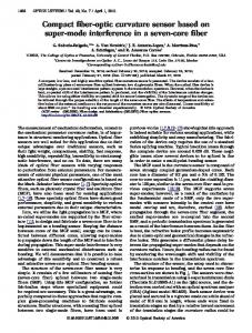
The ever-increasing need for sensing in the chemical and physical domain has led to the development of a variety of sensing schemes, including electrochemical and optical sensors. Optical sensing methods offer many advantages as compared with conventional electronic chemical sensors, such as the high sensitivity, small size, immunity to electromagnetic noise, and amenability to multiplexing. Such schemes can be realized by use of colorimetric (absorptive), vapochromic, or surface plasmon resonance effects implemented in thin films, fiber optics, or waveguide schemes [1]. Alternative optical sensing methods use a remotely transmitted light beam to interact with a lossless material exposed to an analyte. This remote point sensing (RPS) concept is outlined in Fig. 1. A laser beam propagates in free space (or in optical waveguides/fibers), and by interrogating a suitable nanocomposite medium, the “sensor head,” it becomes modulated, thus producing the sensor signal. The sensor head is a powerless (electrically passive) thin-film device of the environmentally sensitive material, not electrically connected to any power or signal processing unit. In a diffractive device, the environmentally induced changes of the optical properties are translated to measureable alterations of the transmitted/reflected diffracted beams. This sensing principle is to be contrasted to the conventional electrochemical sensing and the integratedpath operations such as the light detection and ranging technology [2]. RPS is a low-cost and quite versatile all-optical method featuring spatial localization and remote character of the measurement process. The lack of complicated on-board electrical circuitry and electric connections, the natural immunity to electromagnetic interference, and its ability for sensing in hostile industrial and urban environments (refineries, subways, polluted areas, etc.) are clear advantages. 0146-9592/10/091476-3/$15.00
The enhancement of its response and the optimization of the operational parameters in real-life applications are within the scope of this present contribution. In our recent demonstrations of optical sensors we have provided nanocomposite photonic materials incorporating nanoparticles in inorganic and organic matrices and enabled humidity, methanol, and ammonia sensing [3,4]. In this Letter we present, for the first time to our knowledge, an innovative approach that enhances the performance of the photonic sensor. This is achieved by laser patterning surface relief diffractive elements on the environmentally sensitive optical interface using deep UV pulses. It is demonstrated here that the properties of the SiO2 / NiCl2 diffractive nanocomposite sensor provide enhanced operational means for interrogation and detection of ammonia. The sensing nanocomposite material has been produced by sol-gel methods [5] using tetramethyl orthosilicate (TMOS). NiCl2 nanoparticles were in situ synthesized in the silica matrix by adding NiCl26H2O and stirring. The material was then spin coated on glass substrates to form thin film structures of about 1.4 m thickness. The presence of ammonia in the nickel salt clusters produces complexation and enables the exchange between captured water and diffused ammonia molecules. This effect
Fig. 1. Optical remote-point scheme in both reflectance and transmittance mode. © 2010 Optical Society of America
May 1, 2010 / Vol. 35, No. 9 / OPTICS LETTERS
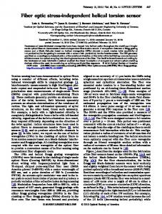
gives rise to variation of the effective refractive index of the material [3], and probably volume fraction changes that affect the geometry, and results in the amendment of the relative optical paths in the diffractive element and respective variation of the diffraction efficiency. The produced materials are environmentally sensitive, their sensing functionality is based on surface interactions, and reactive contact is deleterious to the sensing property itself. Tailoring of the surface morphology is therefore not a trivial issue, and conventional lithographic processing is not suitable. Direct UV etching techniques used here are thus proved to be a unique microfabrication tool. Alternative state-of-the-art patterning methods, which are able to preserve the material properties such as soft lithography, nanoimprint lithography, or scanning probe lithography, could also be exploited in this context [6]. Direct UV laser microetching methods have been implemented for patterning the desired structures. [7]. An ArF excimer laser based microfabrication system allows irradiation of the surface by 5 mJ nanosecond pulses at = 193 nm. It provides high-quality accurate patterning by use of nanopositioners, with minimum penetration depth and negligible thermal loading of the material. A considerable amount of relevant investigations on the laser processing of such materials has been performed. High-quality ablative processing at 60 J / cm2 pulse energy density results in diffraction gratings with spatial period in the range of ⌳ = 10– 100 m fabricated on the sensitive surfaces. A scanning electron micrograph (JEOL 6300) and a surface profile (Tencor Alpha-Step 500IQ) of a typical structure are shown in Fig. 2. The good quality nearly square profile produces clear multiordered diffraction patterns upon laser illumination, of which the zero- or and higher-order diffracted beams may be used for sensor interrogation. Diffractive sensor structures have been experimentally tested to mimic remote photonic sensing operation in the transmission mode. The sensor structure was placed inside the testing chamber and was interrogated using a 5 mW He–Ne laser beam at = 633 nm. A reference beam used provides balance to any laser power fluctuations. The −1, 0, and +1 diffraction orders, as well as the reference beam, were monitored. Ammonia environment is established by inserting small (⬃ microliters) volumes of ammonia in liquid solution followed by evaporation. The original “clean” atmospheric environment is restored by evacuating the chamber after each measurement. The photonic sensor head is positioned for interrogation at ⬃22° beam incidence to attain the experimentally determined maximum responsivity. This geometry, corresponding to the maximum slope of the diffraction efficiency curve, has been verified by a series of real-time recordings at varying incidence. The diffraction angle of the ±1 orders, measured with respect to the zero order, is found at 0.45°, while diffracted beams up to the 10th order were observable. Typical real-time recordings of the transmitted signals are shown in Fig. 3. In the recordings, a
1477
Fig. 2. Scanning electron microscope image of the laser microetched sensor grating 共⌳ = 80 m兲 and the surface profile.
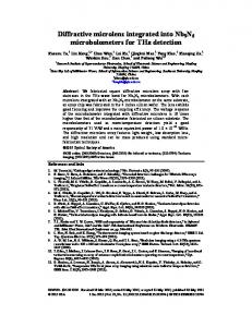
Fig. 3. Temporal response of (a) zero order and (b), (c) ±1 order to 150 ppm of ammonia [shown in (d)].
1478
OPTICS LETTERS / Vol. 35, No. 9 / May 1, 2010
150 ppm ammonia environment is established and is consequently followed by the pure atmospheric ambient. The small apparent bias is vanishing with the outdiffusion of ammonia at a longer time scale, of the order of 15– 20 min. The responsivity of the diffractive sensor is defined as Rm = ⌬m / 共m,0 ␦C兲, which is the normalized variation of the mth-order diffraction efficiency m per unit analyte concentration change ␦C共ppm兲, where m,0 is the diffraction efficiency of the element at the absence of analyte. For a planar unprocessed sensor interface the normalized variation of optical transmission, T, RT = ⌬T / 共T0␦C兲 may be equivalently defined. This definition is also valid and used here for the zero-order undiffracted beam, R0. In Fig. 4, the response of the sensor for various ammonia concentrations for the zero and ±1 order diffraction beams is presented comparatively. The response of the unprocessed planar thin film sensor is recorded by a laser beam incident on the same sample at the same angle of incidence. The measured zero-order responsivity values R0 ⬃ 9.2⫻ 10−5 ppm−1 are found similar to those of the unprocessed planar interface, RT. It is noted here that the expected value due to Fresnel reflection variation is ⬃10−6 ppm−1, and that the observed value is a result of the etalon effect due to the overall film-substrate planar structure. A sixfold responsivity increase for the ±1-order beams is, however, found at R−1 ⬃ 5.3⫻ 10−4 ppm−1
and R+1 ⬃ 2.1⫻ 10−4 ppm−1. The difference between the +1- and −1-order responsivity is attributed to the exact geometry of the diffraction grating combined with the asymmetric readout. It should also be noted here that the ammonia sensor shows a small but traceable response to humidity (0 ppm of ammonia in Fig. 4). The sensor behavior has been verified by applying rigorous coupled-wave analysis using the typical characteristics of the diffractive element and the experimental geometry used. The analysis indicates that a composite refractive index value n ⬃ 1.57 agrees well with the observed behavior and provides an estimate of refractive index change ⌬n / ␦C ⬃ 10−5 ppm−1. The ±1-order response also exhibits a higher signal-to-noise ratio (SNR), defined as the ratio of the diffraction efficiency change over the standard deviation of the signal. SNR for the +1 order is 18.6, as contrasted to the 3.5 found for the zero order. In Fig. 4(b) the low concentration section is presented. It clearly records the lowest detectable value at 2 ppm. It is important to underline here that this is a direct (raw) measurement process and does not involve any lock-in detection or other mathematical estimation methods. In conclusion, a diffractive NiCl2 / SiO2 nanocomposite photonic sensor for ammonia is demonstrated. The device has been fabricated on a thin-film structure using direct UV laser microetching techniques. The diffractive optic sensor has been tested under the RPS scheme at the laboratory environment. The first-order diffracted beams are found to provide an appreciable sensor response at 5.3⫻ 10−4 ppm−1 and SNR⬃ 18.6, which allowed the detection of quite low, 2 ppm, ammonia levels. This is a direct (raw) measurement remote point sensing operation. Work supported by the EU IST ‘‘NANOPHOS’’, Hellenic GSRT PENED ‘‘NYVRIPHOS’’ projects and the ESF-COST MP0604 action. The authors thank Professor M. Sigalas for useful discussions. References
Fig. 4. Response of the diffraction grating sensor to various ammonia concentrations of zero order and ±1 order. The response of the unprocessed planar sensor is shown in the same figure for comparison. (a) Overall response and (b) low ammonia level response is shown.
1. G. C. Righini, A. Tajani, and A. Cutolo, An Introduction to Optoelectronic Sensors (World Scientific, 2009). 2. R. M. Measures, Laser Remote Sensing: Fundamentals and Applications (Krieger, 1992). 3. A. Meristoudi, L. Athanasekos, M. Vasileiadis, S. Pispas, G. Mousdis, E. Karoutsos, D. Alexandropoulos, H. Du, A. Tsigara, K. Kibasi, A. Perrone, and N. A. Vainos, J. Opt. A 11, 8 (2009). 4. A. Tsigara, G. Mountrichas, K. Gatsouli, A. Nichelatti, S. Pispas, N. Madamopoulos, N. A. Vainos, H. L. Du, and F. Roubani-Kalantzopoulou, Sens. Actuators B 120, 481 (2007). 5. A. Lukowiak and W. Strek, J. Sol-Gel Sci. Technol. 50, 201 (2009). 6. B. Gates, Q. Xu, M. Stewart, D. Ryan, G. Willson, and G. Whitesides, Chem. Rev. (Washington, D.C.) 105, 1171 (2005). 7. N. A. Vainos, S. Mailis, S. Pissadakis, L. Boutsikaris, P. J. M. Parmiter, P. Dainty, and T. J. Hall, Appl. Opt. 35, 6304 (1996).