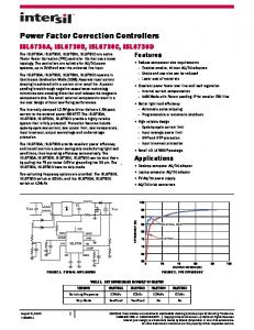
controller for a power factor correction (PFC) converter. The development of the
telecommunications industry and the Internet demands reliable, cost-effective ...
Digital Control For Power Factor Correction Manjing Xie
Thesis submitted to the faculty of the Virginia Polytechnic Institute and State University in partial fulfillment of the requirements for the degree of
Master of Science in Electrical Engineering
Dr. Fred C. Lee, Chair Dr. Alex Q. Huang Dr. Thomas L. Martin
June 2003 Blacksburg, Virginia Keywords: Switch-Mode Power Supply, Digital Control, Power Factor Correction, Feed Forward, Three-Level PFC, Active Balancing
DIGITAL CONTROL FOR POWER FACTOR CORRECTION Manjing Xie
ABSTRACT
This thesis focuses on the study, implementation and improvement of a digital controller for a power factor correction (PFC) converter. The development of the telecommunications industry and the Internet demands reliable, cost-effective and intelligent power. Nowadays, the telecommunication power systems have output current of up to several kiloamperes, consisting of tens of modules. The high-end server system, which holds over 100 CPUs, consumes tens of kilowatts of power. For mission-critical applications, communication between modules and system controllers is critical for reliability. Information about temperature, current, and the total harmonic distortion (THD) of each module will enable the availability of functions such as dynamic temperature control, fault diagnosis and removal, and adaptive control, and will enhance functions such as current sharing and fault protection. The dominance of analog control at the modular level limits system-module communications. Digital control is well recognized for its communication ability. Digital control will provide the solution to system-module communication for the DC power supply. The PFC converter is an important stage for the distributed power system (DPS). Its controller is among the most complex with its three-loop structure and multiplier/divider. This thesis studies the design method, implementation and cost effectiveness of digital control for both a PFC converter and for an advanced PFC converter. Also discussed is the influence of digital delay on PFC performance. A cost-effective solution that achieves good performance is provided. The effectiveness of the solution is verified by simulation.
The three level PFC with range switch is well recognized for its high efficiency. The range switch changes the circuit topology according to the input voltage level. Research literature has discussed the optimal control for both rangeswitch-off and range-switch-on topologies. Realizing optimal analog control requires a complex structure. Until now optimal control for the three-level PFC with analog control has not been achieved. Another disadvantage of the threelevel PFC is the output capacitor voltage imbalance. This thesis proposes an active balancing solution to solve this problem.
iii
ACKNOWLEDGEMENTS I would like to express my sincere appreciation to my advisor, Dr. Fred C. Lee for his guidance, encouragement and continuous support. I would like to thank my master committee members: Dr. Alex Q. Huang for providing me extended knowledge in power IC design, Dr. Thomas L. Martin for helping me develop the basic background for the high-level synthesis method. I must thank all the members of the Center for Power Electronics Systems (CPES) for their friendship, support, discussion and encouragement. My study and research experience in CPES is enjoyable and rewarding. In particular, I would to thank Dr. Yong Li, Dr. Qun Zhao and Dr. Wei Dong for leading me into the field of power electronics and serving as my mentors. Special appreciation goes to Mr. Bing Lu, who helped me with my experiment and shared his research results and knowledge with me. I also extend my appreciation to Mr. Francisco Canales, Mr. Bo Yang, Mr. Shuo Wang, Mr. Liyu Yang, Mr. Nick X. Sun, Mr. Xin Zhang, Mr. Xiaoming Duan, Mr Yang Qiu and Mr. Arthur Ball for their valuable suggestion, comments and discussions. I would like to thank my parents, Kaisheng Xie and Jirong Li for their endless love and support. This work is supported by the National Science Foundation.
iv
TABLE OF CONTENTS ABSTRACT ..........................................................................................................II ACKNOWLEDGEMENTS .................................................................................. IV TABLE OF CONTENTS ...................................................................................... V LIST OF FIGURES ............................................................................................ VII LIST OF TABLES................................................................................................ X 1
INTRODUCTION ...........................................................................................1
1.1
Brief Review of DC Power Supply System ......................................................... 2
1.2
Brief Review of the Digital Signal Processor...................................................... 4
1.3
Goal of Thesis ........................................................................................................ 5
1.4
Task Description ................................................................................................... 6
1.5
Thesis Organization .............................................................................................. 6
2 2.1
REVIEW OF LITERATURE ...........................................................................7 Challenges of Digital Control for PFC................................................................ 7
2.2 Realization of Digital Control .............................................................................. 8 2.2.1 Digital Signal Processor (DSP) Realization of Digital Controller.................. 8 2.2.2 Concurrent Realization of Digital Controller ................................................. 8 2.3
Small-Signal Model for the Low-Frequency Range .......................................... 9
3 DESIGN AND IMPLEMENTATION OF SINGLE SWITCH PFC CONVERTER .....................................................................................................10 3.1 State-of-the-art controller for PFC Converter................................................. 10 3.1.1 PFC Converter .............................................................................................. 10 3.1.2 Review of Control Structure for PFC ........................................................... 12 3.2
Digital Controller for PFC ................................................................................. 23 v
3.2.1 3.2.2 3.2.3
Issues surrounding Digital Control ............................................................... 23 Requirements ................................................................................................ 32 Designing the Digital Controller for PFC..................................................... 39
3.3 Implementation ................................................................................................... 58 3.3.1 Flowchart ...................................................................................................... 58 3.3.2 Experimental Results .................................................................................... 62 3.4 Current-Loop Feed-Forward Compensation ................................................... 64 3.4.1 Input voltage harmonics................................................................................ 65 3.4.2 Influence of input voltage ............................................................................. 65 3.4.3 Current Loop Feed Forward.......................................................................... 71 3.4.4 Simulation Results ........................................................................................ 73 4
DIGITAL CONTROL FOR THE THREE-LEVEL PFC .................................82
4.1
Three-Level PFC Converter .............................................................................. 82
4.2
Literature Review and Previous works............................................................. 83
4.3 Review of 3-LPFC with RS: Operation and Control....................................... 85 4.3.1 Topology at Rsoff mode ............................................................................... 85 4.3.2 Topology at Rson Mode................................................................................ 92 4.4 Control Parameters for Rsoff and Rson modes ............................................... 93 4.4.1 Current Loop Difference and Compensation................................................ 93 4.4.2 Voltage Loop Difference and Compensation ............................................... 94 4.5
Control structure of 3-LPFC Converter........................................................... 95
4.6
Experimental Results.......................................................................................... 96
5
CONCLUSION AND DISCUSSION.............................................................97
5.1
Conclusions.......................................................................................................... 97
5.2
Future Work........................................................................................................ 98
6
REFERENCES ............................................................................................99
APPENDIX I .....................................................................................................104 VITA..................................................................................................................109
vi
LIST OF FIGURES Figure 1 Structure of the distributed power system............................................... 3 Figure 2 Illustration of PF relationship between current and voltage: (a) kθ < 1, k d < 1 , (b) kθ = 1, k d < 1 , (c) kθ < 1, k d = 1 , (d) kθ = 1, k d = 1 ............. 11 Figure 3 Boost Power Factor Correction converter ............................................. 12 Figure 4 Boost PFC converter controller: (a) Boost PFC with controller, (b) Waveforms of input voltage and inductor current, (c) Waveforms of input voltage and output voltage. ...................................................................... 13 Figure 5 Analog average current control For boost-type PFC............................. 14 Figure 6 Small-signal model of current loop........................................................ 15 Figure 7 Small-signal duty-to-current transfer functions...................................... 16 Figure 8 Duty-to-current transfer function and current open loop gain example . 16 Figure 9 Second order filter in feed forward loop ................................................ 17 Figure 10 low-frequency Small-Signal Model for voltage loop ............................ 19 Figure 11 Voltage loop compensation with 45o phase margin ............................ 19 Figure 12 (a) Boost PFC circuit, (b) Input voltage and current waveform, (c) Average Diode forward current waveform ................................................ 21 Figure 13 Quantization effect.............................................................................. 24 Figure 14 Equivalents for quantization effect ...................................................... 24 Figure 15 Noise and disturbance amplitude (a) Original signal and quantized signal, (b) Error signal introduced into system. ........................................ 25 Figure 16 complete control systems for the PFC current loop ............................ 25 Figure 17 (a) square waveform and (b) harmonic components .......................... 27 Figure 18 Saw tooth waveform and (b) harmonic components........................... 28 Figure 19 Frequency response of sample-and-hold function with 100KHz sampling frequency. ................................................................................. 30 Figure 20 Effect of digital delay........................................................................... 31 Figure 21 Sampling a 20Hz sinusoidal wave at 25 Hz sampling frequency ........ 31 Figure 22 Illustration of the aliasing effect in frequency domain (a) Signal spectrum, (b) Sampling frequency and (c) Wrap around spectrum .......... 32 Figure 23 Noise introduced by ADC.................................................................... 33 Figure 24 Fundamental harmonic and ADC resolution. ...................................... 35 Figure 25 harmonic ratios for semi sinusoidal wave ........................................... 36 Figure 26 Illustration of disturbance introduced by digital PWM ......................... 37 Gid Figure 27 Bode plot for ...................................................................... 38 1 + CGid K i Figure 28 Digital control structure of single-switch PFC...................................... 40 Figure 29 Power stage of Boost PFC.................................................................. 41 Figure 30 Bit weighting for Q-15 Format [40]. ..................................................... 42 Figure 31 Poles and zeros in the z-plane............................................................ 44 Figure 32 Power stage with sample and hold ..................................................... 45 Figure 33 Duty to current transfer function mapped into z-plane ........................ 45
vii
Figure 34 Comparison of the discrete model and continuous model .................. 46 Figure 35 Current loop with digital compensator................................................. 47 Figure 36 Bode plot for current open loop gain with one zero compensation ..... 48 Figure 37 Input current waveform with one-zero digital current compensator..... 49 Figure 38 Current Open loop Bode plot with two zeros compensation ............... 50 Figure 39 Feed forward loop............................................................................... 52 Figure 40 Bode plot of the low-pass filter............................................................ 52 Figure 41 Bode plot for low-pass filter................................................................. 54 Figure 42 Outer voltage loop .............................................................................. 55 Figure 43 Bode plot for voltage open loop gain .................................................. 57 Figure 44 Flowchart of main program ................................................................. 58 Figure 45 Flowchart for interrupt service routine program .................................. 59 Figure 46 Flowchart for current compensator subprogram ................................. 60 Figure 47 Flowchart for voltage compensator subprogram................................. 61 Figure 48 Flowchart for feed forward loop subprogram ...................................... 62 Figure 49 Input Current waveform w/o EMI filter................................................. 63 Figure 50 Simplified current loop system with input voltage influence. ............... 65 Figure 51 Bode plots of Givclose with different current compensator ..................... 68 Figure 52 Relationship between voltage 2nd harmonic and line current: (a) line voltage, (b) boost converter input voltage, (c) 2nd harmonic voltage and 2nd harmonic current and (d) fundamental and 3rd harmonics generated....... 69 Figure 53 Current vectors and voltage vector ..................................................... 70 Figure 54 Illustration of current-loop feed-forward .............................................. 71 Figure 55 Effect of different CFF gain k vi ............................................................ 72 Figure 56 Line current of PFC w/o EMI filter ( f c =8KHz)..................................... 73 Figure 57 Line current of PFC w/o EMI filter ( f c =4KHz)..................................... 74 Figure 58 Line current of PFC w/o EMI filter ( f c =4KHz, w/ k vi = 0.9 ) ................. 74 Figure 59 Comparison of line-current harmonics with different current loop bandwidths. .............................................................................................. 75 Figure 60 Comparison of line current harmonics with and without CFF.............. 76 Figure 61 harmonic comparisons........................................................................ 76 Figure 62 Bode plots for k vi ⊂ (0,1) ..................................................................... 78 Figure 63 Bode plots for k vi ⊂ (1,2) ..................................................................... 78 Figure 64 Comparison of displacement angles (degree) and displacement factors with different CFF gain. ............................................................................ 79 Figure 65 Line current w/o EMI filter ( f c =4KHz, w/o CFF) ................................. 80 Figure 66 Line current w/o EMI filter ( f c =4KHz, w/ CFF k vi = 0.9 )...................... 80 Figure 67 Line Current Harmonics Comparison.................................................. 81 Figure 68 Power stage of 3-LPFC w/ RS ............................................................ 83 Figure 69 Efficiency comparisons between conventional Single-switch PFC and analog controlled 3-LPFC......................................................................... 84 Figure 70 Converter topology at Rsoff mode: (a) Original topology and (b) simplified topology.................................................................................... 85 Figure 71 Passive balancing with balancing resistors......................................... 86 viii
Figure 72 Average model of 3-LPFC at Rsoff mode. .......................................... 87 Figure 73 Small-signal model of 3-LPFC at Rsoff mode. .................................... 87 Figure 74 PWM operation in Rsoff mode: (a) Duty cycle >50% and (b) Duty cycle