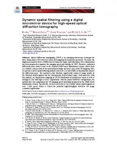
micromachines Article
Digital Micromirror Device (DMD)-Based High-Cycle Torsional Fatigue Testing Micromachine for 1D Nanomaterials Chenchen Jiang 1,2 , Dayong Hu 1,3 and Yang Lu 1,2, * 1 2 3
*
Department of Mechanical and Biomedical Engineering, City University of Hong Kong, Kowloon, Hong Kong, China;
[email protected] (C.J.);
[email protected] (D.H.) Center for Advanced Structural Materials (CASM), Shenzhen Research Institute, City University of Hong Kong, Shenzhen 518057, China Department of Aircraft Airworthiness Engineering, School of Transportation Science and Engineering, Beihang University, Beijing 100191, China Correspondence:
[email protected]; Tel.: +852-3442-4061
Academic Editors: Toshio Fukuda, Mohd Ridzuan bin Ahmad and Nam-Trung Nguyen Received: 31 October 2015; Accepted: 7 March 2016; Published: 14 March 2016
Abstract: Fatigue behavior of nanomaterials could ultimately limit their applications in variable nano-devices and flexible nanoelectronics. However, very few existing nanoscale mechanical testing instruments were designed for dedicated fatigue experiments, especially for the challenging torsional cyclic loading. In this work, a novel high-cycle torsion straining micromachine, based on the digital micromirror device (DMD), has been developed for the torsional fatigue study on various one-dimensional (1D) nanostructures, such as metallic and semiconductor nanowires. Due to the small footprint of the DMD chip itself and its cable-remote controlling mechanisms, it can be further used for the desired in situ testing under high-resolution optical or electron microscopes (e.g., scanning electron microscope (SEM)), which allows real-time monitoring of the fatigue testing status and construction of useful structure-property relationships for the nanomaterials. We have then demonstrated its applications for testing nanowire samples with diameters about 100 nm and 500 nm, up to 1000 nm, and some of them experienced over hundreds of thousands of loading cycles before fatigue failure. Due to the commercial availability of the DMD and millions of micromirrors available on a single chip, this platform could offer a low-cost and high-throughput nanomechanical solution for the uncovered torsional fatigue behavior of various 1D nanostructures. Keywords: microelectromechanical systems (MEMS); nanomechanics; nano-fatigue; digital micromirror device (DMD); torsion; nanowire
1. Introduction Due to their importance as building blocks for nanoscale electronics and electro-mechanical systems in numerous advanced engineering applications, such as flexible electronics/wearable electronics, bio-integrated electronics [1–4], one-dimensional (1D) nanoscale materials and structures, such as nanowires and nanotubes, have been extensively investigated in the past decades [5–7]. However, the ability to achieve the full potential of aforementioned new technologies in these fascinating applications is ultimately limited by the mechanical reliability of these one-dimensional building blocks [8–12]. In particular, fatigue, or the progressive and localized structural damage that occurs when a material is subjected to cyclic loading, is a commonly encountered mode of failure in nanomaterial components, which ultimately determines their device stability and lifetime. Despite substantial research that has been recently devoted to the fatigue behavior of individual 1D nanostructures subjected to cyclic tensile or bending loading [13–18], torsional fatigue testing Micromachines 2016, 7, 49; doi:10.3390/mi7030049
www.mdpi.com/journal/micromachines
Micromachines 2016, 7, 49
2 of 9
remains little reported, largely due to the challenges of performing high cyclic torsional loading on such exceedingly small samples. Therefore, designing and developing of appropriate testing platforms are the greatest challenges in the current nanomechanics community. Recently, microelectromechanical systems (MEMS)-based testing platforms have emerged as powerful and versatile tools to interrogate low-dimensional micro- and nanostructures, and a number of MEMS devices have been successfully developed to investigate the mechanical strength and plastic deformation for various kinds of 1D nanomaterials [19–21]. However, the dynamic characterization for important fatigue behavior, especially torsional fatigue, remains highly challenging, mainly due to the inherent limitations of existing MEMS designs, such as the loading frequency is not high enough for prolonged fatigue experiments, and the out-plane movement is not available for torsional straining. Here, instead of designing a dedicated MEMS device, we adopted a commercially available MEMS product DMD (Digital Micromirror Device, by Texas Instruments, Dallas, TX, USA) for the desired cyclic torsional loading for individual nanowires [22–24], and used this innovative platform to study the intriguing high-cycle fatigue behavior for a few representative nanowire samples. 2. Platform Development and Methodology Our platform was based on a customized Digital Light Processing (DLP) development kit from Texas Instrument, which was originally developed for programming and controlling the operation of DMD for various advanced optical/display applications [25]. Inside the DMD is a micro-electro-mechanical system (MEMS) consisting of hundreds of thousands of over one million of tiny switchable micro-mirrors with two stable mirror states (for example, +12˝ and ´12˝ for most DMD devices) as shown in Figure 1b [26]. In the present work, the 0.7” 1024 ˆ 768 Extended Graphics Array (XGA) TI DMD was used, in which the micromirrors were attached to the underlying torsion hinges as shown in Figure 1c. Under the effects of electrode potential, the mirror could be electrostatically attracted to address electrodes with the largest electrostatic field potential when bias/reset voltage was applied on it [27]. The mirror rotated until it came to rest against mechanical stops which limits the mirror rotation angle to +12˝ or ´12˝ . Due to these characteristics, the rotation direction of individual micromirrors was fully controllable through input programming. For the purpose of mechanical loading, the tilting movement of the micromirrors in DMD could be used in applying torsional load on the individual 1D nanostructures, such as nanowires with diameters ~100–500 nm (or even larger) if they were positioned properly. Specifically, torsional deformation of nanowires/nanotubes could be realized by aligning and clamping the sample along the tilting (hinge) axis of the micromirrors (as shown in Figure 1e, which showed the corresponding out-of-plane movement). The maximum twisting angle of the sample could be totally 24˝ , when two mirrors were fully tilted toward the opposite directions (+12˝ for one mirror and ´12˝ for another mirror). The maximum torsional strain can be then calculated as torsion strain γ = r¨ ϕ/L, where r is the sample radius, ϕ is the total torsion radian, L is gauge length of the sample (the actual strain depends on the true loading state when the nanowire samples were deformed). From Figure 1g,h, it is easy to find that the shear strain of nanowire is proportional to its radius and inversely proportional to its gauge length. Figure 2 shows the entire micromachine platform and their respective arrangement for testing under an optical microscope. After removing the kovar metal frame from the DMD, the nanowire specimen would be clamped onto the micromirrors with epoxy by a high-precision nanomanipulator. In order to achieve pure torsion, the axis of the nanowire should be well aligned along with the torsion hinge precisely. The bonding of the nanowire with the micromirror should be firm (each glue spot size about 2 µm) to avoid misalignment and sliding issues. The optical microscope which connected with a high-speed camera was used to capture the in situ image of the nanowire under loading. The state of each micromirror could be controlled by our customized software with Graphical User Interface (GUI) on the computer. During operation, the DLP circuit board controlling system decoded the programming information from the computer into the bit stream read by the DMD. The loading cycles and loading frequency could be input from the software easily. As the micromirror flipping frequency
Micromachines 2016, 7, 49
board controlling Micromachines 2016, 7, 49system
3 of 9
decoded the programming information from the computer into the 3 ofbit 9 stream read by the DMD. The loading cycles and loading frequency could be input from the software easily. As the micromirror flipping frequency could be up to thousands of Hz, this platform could up tofor thousands of Hz, this platform is testing well suited desired fatigue testing is wellbe suited the desired high-cycle fatigue (andfor thethe DMD was high-cycle proved to be reliable and (and the DMD was proved to be reliable and stable after billions of operations [24]). stable after billions of operations [24]).
Figure 1. 1. Scheme Scheme of of the the DMD-based DMD-based torsional torsional testing testing micromachine: micromachine: (a) (a) shows shows the the DMD DMD chip chip after after Figure removing the protection cover; (b) SEM image shows that millions of micromirror arrays are removing the protection cover; (b) SEM image shows that millions of micromirror arrays are available available a single chip, withnanowire one single red clamped square) being clamped between on a singleon DMD chip, DMD with one single (in nanowire red square)(in being between two diagonally two diagonally opposite (c) shows thestructure micro-fabricated structure under a whose single opposite micromirrors; (c) micromirrors; shows the micro-fabricated under a single micromirror, micromirror, whose main components were torsion hinge and electrodes. Side view (d) shows how main components were torsion hinge and electrodes. Side view (d) shows how the electrostatic force the electrostatic force between the mirror and the underneath electrodes actuate the micromirror. between the mirror and the underneath electrodes actuate the micromirror. The schematic illustration Theshows schematic illustration shows howtilting two along diagonal micromirrors tiltingthe along the hinge can (e) how two diagonal(e) micromirrors the hinge can introduce torsional straining introduce the torsional straining on the(f). nanowire clamped (f).relationship Graph (g) and (h) illustrate on the nanowire clamped in-between Graph (g) and (h)in-between illustrate the between shear the relationship strain and radius or gauge length. strain and radiusbetween or gaugeshear length.
Micromachines 2016, 7, 49 Micromachines 2016, 7, 49 Micromachines 2016, 7, 49
4 of 9 4 of 9 4 of 9
Figure 2. Experimental setup under an optical microscope: The micromanipulator (A) was used to Figure 2. 2. Experimental Experimentalsetup setupunder under optical microscope: The micromanipulator (A) was to used to Figure anan optical microscope: Thewhich micromanipulator (A) was bond nanowire onto the micromirrors of DMD chip (B), connected with the used digital bond light bond nanowire onto the micromirrors of DMD chip (B), which connected with the digital light nanowire the circuit micromirrors of DMD chip cable. (B), which connected with the the digital lightDMD processing processingonto (DLP) board (C) via data In order to control individual pixel processing circuit (C) via data cable. In order to control the pixel individual DMD pixel (DLP) circuit(DLP) board viaboard data cable. In order to control the DMD (micromirror), the (micromirror), the (C) customized programming software (D)individual will transmit the binary signal to (C). (micromirror), the customized programming software (D) willsignal transmit theDuring binarythe signal to (C). customized programming software (D) will transmit the binary to (C). testing, the During the testing, the real time images (E) will be captured by a high magnification optical During testing, the be real time images (E)magnification will be captured a high magnification real timethe images (E) will captured by a high opticalbymicroscope (F) equipped optical with a microscope (F) equipped with a high-speed camera. microscope (F) equipped with a high-speed camera. high-speed camera.
Most importantly, because of its small footprint and the cable-remote controlling mechanisms, Most importantly, because of its small footprint and the cable-remote controlling mechanisms, Most importantly, because of itscan small cable-remote mechanisms, this this DMD-based testing platform be footprint ideal for and the the in situ scanning controlling electron microscope (SEM) this DMD-based testing platform can be ideal for the in situ scanning electron microscope (SEM) DMD-based testing platform can be ideal for the in situ scanning electron microscope (SEM) testing, testing, allowing the real time observation of materials responses under torsion cyclic loading. This testing, allowing the real time observation of materials responses under torsion cyclic loading. This allowing the most real time observation of of materials responses under in torsion cyclic loading. This is one of is one of the attractive features our platform as showed Figure 3. With a customized SEM is one of the most attractive features of our platform as showed in Figure 3. With a customized SEM the most attractive features of our platform as showed in Figure 3. With a customized SEM port for port for cable communication and remote control, we have successfully managed to put the DMD port for cable communication and remote control, we have successfully managed to put the DMD cable control, weFEG have successfully managed to put DMD into ainside high into acommunication high resolution and SEMremote (FEI Quanta 450 SEM, Hillsboro, OR, USA) andthe made it work into a high resolution SEM (FEI Quanta 450 FEG SEM, Hillsboro, OR, USA) and made it work inside resolution the SEM. SEM (FEI Quanta 450 FEG SEM, Hillsboro, OR, USA) and made it work inside the SEM. the SEM.
Figure 3. 3. In in (a) is connected Figure In situ situ SEM SEM testing testing set-up: set-up: the the digital digital light light procession procession (DLP) (DLP) circuit circuit board board Figure 3. In situ SEM testing set-up: the digital light procession (DLP) circuit board in in (a) (a) is is connected connected with the (b) DMD chip inside the SEM chamber through a data cable. The compact size of the the DMD with with the the (b) (b) DMD DMD chip chip inside inside the the SEM SEM chamber chamber through through aa data data cable. cable. The The compact compact size size of of the DMD DMD chip unit can ensure the remote operation via the data cable inside the SEM. chip unit can ensure the remote operation via the data cable inside the SEM. chip unit can ensure the remote operation via the data cable inside the SEM.
3. Platform 3. PlatformDemonstration Demonstrationand andResults Results Platform Demonstration and Results Based on this platform, cyclic torsional tests of nanowire samples samples with with different different diameters diameters and and Based on this platform, platform, cyclic torsional tests of nanowire nanowire diameters gauge length length have have been been demonstrated. demonstrated. The samples were always recorded before gauge The SEM SEM images images of of the the samples were always recorded before torsional fatigue tests. The effective torsion gauge length depended on the distance between the two torsional fatigue fatigue tests. tests.The Theeffective effectivetorsion torsion gauge length depended distance between the gauge length depended on on the the distance between the two glue clamping positions. The torsion test could be observed by the high-speed camera which two clamping positions. torsion could observedby bythe the high-speed high-speed camera camera which glueglue clamping positions. TheThe torsion testtest could bebeobserved which connected to to the microscope microscope (opticalororSEM). SEM). In ordertotomake makeit iteasy easy distinguish three states connected toto distinguish thethe three states of connected to the the microscope(optical (optical or SEM).InInorder order to make it easy to distinguish the three states of micromirrors according to brightness, we tilted the DMD a little bit with respect to the projecting micromirrors according to brightness, we tilted the DMD a little bit with respect to the projecting light. of micromirrors according to brightness, we tilted the DMD a little bit with respect to the projecting light. It could be defined if the micromirror became very bright, it meant on flat/ground It could be defined that if that the micromirror became very bright, it meant it was it onwas flat/ground state, light. It could be defined that if the micromirror became very bright, it meant it was on flat/ground state, which could reflect more light into the microscope. If the micromirror became veryitdark, it which could reflect more light into the microscope. If the micromirror became very dark, meant state, which could reflect more light into the microscope. If the micromirror became very dark, it meant the micromirror flipped to “off” state or its angle was −12°, which reflected much of the light ˝ , which reflected much of the light off the the micromirror flippedflipped to “off”to state orstate its angle ´12was meant the micromirror “off” or itswas angle −12°, which reflected much of the light off the microscope. If the micromirror was gray (in between the two above states), it meant the off the microscope. If the micromirror was gray (in between the two above states), it meant the
Micromachines 2016, 7, 49 Micromachines 2016, 7, 49
5 of 9 5 of 9
microscope. the micromirror was or gray between the two above states),some it meant thelight micromirror micromirror Ifflipped to “on” state its (in angle was 12°, which reflected of the into the flipped to “on” or itsthat angle 12˝ ,state. which reflected some of the light into the microscope but less microscope butstate less than ofwas the flat than that of the flat state. 3.1. Demonstration of the Cyclic Loading with Different Loading Amplitudes 3.1. Demonstration of the Cyclic Loading with Different Loading Amplitudes We firstly demonstrated the torsional twisting of a silver nanowire with diameter ~100 nm and Welength firstly demonstrated the(see torsional of a silver nanowire withIn diameter ~100only nm and gauge ~25 μm by 12° also twisting the Supplementary Video S1). this case, one ˝ gauge length needed ~25 µm to by flip, 12 (see also the Supplementary Video S1).way In this onlystate one as micromirror micromirror while another one was fixed all the (at case, ground shown in needed to flip, whilethe another fixed all the ground as shown in Figure 4). another During Figure 4). During test, one the was micromirror at way the (at upper left state corner was fixed, while the test, the micromirror the firstly upperflipped left corner was fixed, another micromirror at flipped the lower micromirror at the lower at right to positive 12° while (Figure 4b), and then quickly to ˝ (Figure 4b), and then quickly flipped to negative 12˝ (Figure 4c). As right firstly flipped to positive 12 negative 12° (Figure 4c). As a result, repeating processes of (b) and (c) alternatively will induce the atorsion result, loading repeating of (b) and (c) alternatively induce torsion loading onprocesses the nanowire. Under this loadingwill pattern, thethe frequency could on be the up nanowire. to 50 Hz. Under this loading pattern, frequency could upHz) to 50 Hz.0.04% After shear more than one loading After more than one millionthe loading cycles (8 h be × 50 with strain, themillion nanowire still cycles (8 h ˆ 50 Hz) with 0.04% shear strain, the nanowire still did not break. did not break.
˝ : (a) Figure 4. 4. Cyclic torsional loading loading on on aa nanowire nanowire with with twisting twisting angle angle of of 12 12°: the SEM SEM image image Figure Cyclic torsional (a) shows shows the ˝ in of the the 100 100 nm nm nanowire nanowire sample sample after after the the test. test. The The lower lower right right mirror mirror flipped flipped to to 12 12° of in (b) (b) then then quickly quickly flipped to to ´12 −12°˝in flipped in(c). (c).Repeating Repeatingthe theprocesses processes of of (b) (b)and and (c) (c) alternatively alternatively will will induce induce the the cyclic cyclic torsion torsion loading on the nanowire sample. sample.
To further demonstrate that this micromachine could be versatile for various 1D nanomaterials To further demonstrate that this micromachine could be versatile for various 1D nanomaterials with different sizes, another nanowire sample with diameter ~500 nm and gauge length ~25 μm was with different sizes, another nanowire sample with diameter ~500 nm and gauge length ~25 µm was also tested, but the torsion angle was 24° this time (see also the Supplementary Video S2). Figure 5 also tested, but the torsion angle was 24˝ this time (see also the Supplementary Video S2). Figure 5 showed how the nanowire with diameter of 500 nm was twisted by DMD micromirrors during a full showed how the nanowire with diameter of 500 nm was twisted by DMD micromirrors during a full loading cycle as we designed (the “on” state is brighter than “off” state in this figure). The nanowire loading cycle as we designed (the “on” state is brighter than “off” state in this figure). The nanowire was very straight and boned precisely along the axis of hinge before the experiment as Figure 5a was very straight and boned precisely along the axis of hinge before the experiment as Figure 5a shows. shows. In Figure 5b, which was named as the loading process, the micromirror at the upper left In Figure 5b, which was named as the loading process, the micromirror at the upper left corner flipped corner flipped to negative 12°, the micromirror at the lower right corner flipped to positive 12°. The to negative 12˝ , the micromirror at the lower right corner flipped to positive 12˝ . The nanowire would nanowire would be twisted by 24° in total, which was the maximum twisting angle our platform can be twisted by 24˝ in total, which was the maximum twisting angle our platform can provide (fairly provide (fairly enough for most torsional fatigue studies). In Figure 5c, the upper one returned to flat enough for most torsional fatigue studies). In Figure 5c, the upper one returned to flat state, and the state, and the lower one stayed at the negative 12° position. Then, in Figure 5d, both of the two lower one stayed at the negative 12˝ position. Then, in Figure 5d, both of the two micromirrors became micromirrors became flat. Figure 5c,d could be called the unloading process, in which the nanowire flat. Figure 5c,d could be called the unloading process, in which the nanowire would become stress would become stress free. In Figure 5e, the loading process started again and both of them would free. In Figure 5e, the loading process started again and both of them would quickly flip to ´12˝ and quickly flip to −12° and 12°, respectively, at the same time. However, the unloading process in Figure 12˝ , respectively, at the same time. However, the unloading process in Figure 5f became different. The 5f became different. The upper one remained statically at negative 12° position, but the lower one upper one remained statically at negative 12˝ position, but the lower one flipped back to flat state. At flipped back to flat state. At last, the upper one flipped back to flat as shown in Figure 5g. They last, the upper one flipped back to flat as shown in Figure 5g. They would always repeat this loading would always repeat this loading pattern, as long as the DMD was running, to maintain the fatigue pattern, as long as the DMD was running, to maintain the fatigue straining process. Because this straining process. Because this loading pattern included more steps than that of Figure 4, its loading pattern included more steps than that of Figure 4, its frequency was slightly lower and was frequency was slightly lower and was about 20 Hz in this case. In addition, after almost 576,000 about 20 Hz in this case. In addition, after almost 576,000 loading cycles (8 h ˆ 20 Hz) with shear strain loading cycles (8 h × 20 Hz) with shear strain about 0.42%, the nanowire still stayed original as about 0.42%, the nanowire still stayed original as Figure 5h shows, indicating good fatigue resistance. Figure 5h shows, indicating good fatigue resistance.
Micromachines 2016, 7, 49 Micromachines 2016, 7, 49 Micromachines 2016, 7, 49
6 of 9 6 of 9 6 of 9
Figure 5. Cyclictorsional torsionalloading loading on on a nanowire nanowire with with maximum 24° (b)(b) to to (g),(g), thethe Figure 5. Cyclic 24˝twisting: twisting:From From Figure 5. Cyclic torsional loading on aa nanowire with maximum maximum 24° twisting: From (b) to (g), the rotation angle changes as the picture shows. The maximum total torsion angle is 24° in this case ˝ rotation angle angle changes changes as as the The maximum maximum total total torsion torsion angle angle is is 24° 24 in in this this case case rotation the picture picture shows. shows. The (12° + 12°), with two diagonal mirrors titled in opposite directions. (a) shows the original nanowire ˝ + 12 ˝ ), with (12 two diagonal mirrors titled in opposite directions. (a) shows the original nanowire (12° + 12°), with two diagonal mirrors titled in opposite directions. (a) shows the original nanowire with diameter ~500 nm before the test. (h) shows the same nanowire after the test. with diameter diameter ~500 ~500 nm nm before before the the test. test. (h) (h) shows shows the the same same nanowire nanowire after after the the test. test. with
3.2. Demonstration of the Fatigue Failures of Nanowires under Cyclic Torsional Loading 3.2. Demonstration Demonstration of of the the Fatigue Fatigue Failures Failures of of Nanowires Nanowires under 3.2. under Cyclic Cyclic Torsional Torsional Loading Loading In order to increase the relative loading amplitude (e.g., shear strain) and see if the nanowire the relative loading strain) nanowire In order amplitude (e.g., shear seeofif the the 100 sample can to beincrease indeed fractured during torsional fatigue tests, the strain) gauge and length nm sample can be indeed fractured during torsional fatigue tests, the gauge length of the 100 nm can nanowire be indeed fractured during torsional length of the 100 diameter was decreased to about 1 μm. fatigue Figure 6tests, showsthe thegauge nanowire before anddiameter afternm nanowire was decreased to about 1 µm. Figure 6 shows theoptical before and cyclic loading diameter nanowire wasand decreased to about 1 done μm. Figure 6nanowire shows the nanowire before and after cyclic loading testing, the experiment was under microscope. Theafter twisting pattern testing, and the experiment was done under optical microscope. The twisting pattern was similar cyclic loading testing, and the experiment was done under optical microscope. The twisting pattern was similar as Figure 5. However, the nanowire fractured after about 432,000 (6 h × 20 Hz) of as loading Figure 5. However, theHowever, nanowire fractured after aboutthe 432,000 (6 before h ˆ 432,000 20and Hz)after of cycles was similar as Figure 5. the nanowire fractured after about (6 loading hthe × 20 cycles with shear strain about 2.1%. We examine sample testHz) by of with shear strain about 2.1%. We examine theWe sample before and after with the test by SEM imaging SEM imaging and confirmed theabout fatigue2.1%. failure of examine the nanowire sample torsional fatigue. loading cycles with shear strain the sample before and after the testand by confirmed theand fatigue failure of nanowire sample torsional fatigue. SEM imaging confirmed thethe fatigue failure of thewith nanowire sample with torsional fatigue.
Figure 6. A Ag Nanowire with ~100 nm diameter has fractured after cyclic torsional loading: (a) shows the nanowire before the test. (b) shows the sample right after torsional fatigue failure after Figure 6. with ~100 nmnm diameter has fractured after cyclic torsional loading: (a) Figure 6. Acycles. AAg AgNanowire Nanowire with ~100 diameter fractured after loading: ~432,000 Note that the difference in contrast for has the bonding points incyclic (a) andtorsional (b) was due to shows the nanowire before the test. (b) shows the sample right after torsional fatigue failure after (a)the shows the nanowire before the test. (b) shows theimaging sample the right after torsional fatigue used failure different electron beam voltages we used for SEM sample. We intentionally ~432,000 cycles. Note Note that the in contrast for the points in (a) and(a), (b)while waswas due to low~432,000 e-beam voltage (2 kV) for boundary of bonding clamping points the after cycles. thatdifference the quantifying difference inthe contrast for bonding the points in in (a) and (b) due the different electron beam voltages we imaging sample. We intentionally used points appeared more “transparent” under high electronthe beam voltage kV) in (b) and to bonding the different electron beam voltages weused usedfor forSEM SEM imaging the sample. We(10 intentionally used low e-beam voltage (2 kV) for quantifying the boundary of clamping points in (a), while the (c). (c) shows the close-up view of the fractured nanowire after stopped the test. low e-beam voltage (2 kV) for quantifying the boundary of clamping points in (a), while the bonding bonding points appeared more “transparent” under high electron beam voltage (10 kV) in (b) and points appeared more “transparent” under high electron beam voltage (10 kV) in (b) and (c). (c) shows in SEM torsion fatigue tests were also successfully, despite the (c). (c) showsview thesitu close-up view of nanowire the fractured after stopped the test. theSimilarly, close-up of the fractured afternanowire stopped thedemonstrated test.
dynamic in situ SEM imaging quality being low (in order to maintain the frame/scanning rate). Similarly, in also situ the SEM torsion fatigue tests demonstrated insuccessfully, despiteofthe Figure 7a,b (see Supplementary Video S3)were showalso the corresponding situ torsion loading Similarly, in situ SEM torsion fatigue tests were also demonstrated successfully, despite the a Ag nanowire in SEM. Exceptquality for the loading pattern, the diameter of thethe nanowire (100 nm), the dynamic in situ SEM imaging being low (in order to maintain frame/scanning rate). dynamic in situ SEM imaging quality being low (in order to maintain the frame/scanning rate). gauge length (1 μm) and torsion radian (24°) were all similar to Figure 6. The loading frequency, Figure 7a,b (see also the Supplementary Video S3) show the corresponding in situ torsion loading of Figure 7a,b (see also the Supplementary Video S3) show the corresponding in situ torsion loading of a which was about 30 Hz,Except was faster thanloading that of Figure 6. With the help of in SEM, the(100 number a Ag nanowire in SEM. for the pattern, the diameter thesitu nanowire nm),ofthe Agloading nanowire in SEM. Except for the loading pattern, the diameter of the nanowire (100 nm), the gauge cycles fracture became easier obtain. moment of fracture, as loading Figure 7bfrequency, shows, gauge length (1 before μm) and torsion radian (24°)towere allThe similar to Figure 6. The ˝ length (1 µm) and torsion radian (24 ) were all similar to Figure 6. The loading frequency, which was
which was about 30 Hz, was faster than that of Figure 6. With the help of in situ SEM, the number of loading cycles before fracture became easier to obtain. The moment of fracture, as Figure 7b shows,
Micromachines 2016, 7, 49
7 of 9
about 30 Hz, was faster than that of Figure 6. With the help of in situ SEM, the number of loading cycles Micromachines 2016, 7, 49 7 of 9 before fracture became easier to obtain. The moment of fracture, as Figure 7b shows, was captured during the torsion test,the after abouttest, 378,000 h ˆ378,000 30 Hz)(3.5 loading cycles shear strain at about was captured during torsion after (3.5 about h × 30 Hz) with loading cycles with shear 2.1%. In addition, due to there being millions of mirrors on a single chip and them being able to be strain at about 2.1%. In addition, due to there being millions of mirrors on a single chip and them operated individually and independently, we could potentially test many samples at the same time, by being able to be operated individually and independently, we could potentially test many samples clamping and testing them on and different micro mirrors on themicro chip, which speed the whole at the same time, by clamping testing them on different mirrorscould on the chip,up which could fatigue study process in the future. speed up the whole fatigue study process in the future.
(a)
(b)
Figure 7. 7. In always tilted tilted Figure In situ situ SEM SEM torsional torsional fatigue fatigue testing testing of of aa 100 100 nm nm Ag Ag nanowire: nanowire: the the two two mirrors mirrors always towards the opposite directions in each cycle. In (a) mirror A flipped to 12° and mirror B flipped to towards the opposite directions in each cycle. In (a) mirror A flipped to 12˝ and mirror B flipped to −12°.˝ .After ´12 Afteralmost almostfour fourhours hoursof ofcyclic cyclicloading, loading,the thenanowire nanowirefractured fracturedlike like(b). (b).
3.3. Quantifying the Strain Distribution along the Nanowire under Torsion 3.3. Quantifying the Strain Distribution along the Nanowire under Torsion Lastly, to quantify the strain distribution in the sample during torsion straining, finite element Lastly, to quantify the strain distribution in the sample during torsion straining, finite element method (FEM) modeling is needed. Here, we used commercial software (ABAQUS) to simulate the method (FEM) modeling is needed. Here, we used commercial software (ABAQUS) to simulate nanowire torsional deformation actuated by the DMD tilting movements. One set of the simulation the nanowire torsional deformation actuated by the DMD tilting movements. One set of the results was shown in Figure 8, indicating that the nanowires experienced relatively uniform simulation results was shown in Figure 8, indicating that the nanowires experienced relatively deformation under pure torsional loading along their length direction. For the three kinds of uniform deformation under pure torsional loading along their length direction. For the three kinds demonstrated nanowire torsional testing experiments, the estimated max shear strain was ~0.04% of demonstrated nanowire torsional testing experiments, the estimated max shear strain was ~0.04% for 100 nm silver nanowire (gauge length about 25 μm and torsion radian of 0.21 rad), ~0.42% for the for 100 nm silver nanowire (gauge length about 25 µm and torsion radian of 0.21 rad), ~0.42% for the 500 nm nanowires (gauge length about 25 μm and torsion radian of 0.42 rad), and ~2.1% for the 500 nm nanowires (gauge length about 25 µm and torsion radian of 0.42 rad), and ~2.1% for the 100 nm 100 nm nanowires (gauge length about 1 μm and torsion radian of 0.42 rad), respectively. The shear nanowires (gauge length about 1 µm and torsion radian of 0.42 rad), respectively. The shear strain of strain of nanowire in Figure 3 was the same as that of Figure 7. In the future, the shear strain could nanowire in Figure 3 was the same as that of Figure 7. In the future, the shear strain could be further be further elevated by adjusting the gauge length of the nanowire samples between the clamping elevated by adjusting the gauge length of the nanowire samples between the clamping points during points during the bonding process and/or by increasing the diameter of the samples (see also the the bonding process and/or by increasing the diameter of the samples (see also the Supplementary Supplementary Video S4). It could be also seen that the maximum von Mises stress occurred at the Video S4). It could be also seen that the maximum von Mises stress occurred at the edge of the nanowire edge of the nanowire and the lowest at the center of it, agreeing well with our expectation and solid and the lowest at the center of it, agreeing well with our expectation and solid mechanics theory. In mechanics theory. In the long run, assisted by real time SEM imaging, the FEM analysis will be the long run, assisted by real time SEM imaging, the FEM analysis will be beneficial for precisely beneficial for precisely quantifying the fatigue strain limit of the nanomaterial samples and for quantifying the fatigue strain limit of the nanomaterial samples and for in-depth investigating of their in-depth investigating of their failure mechanisms during the torsional loading. failure mechanisms during the torsional loading. In the future, the frequency of the torsion loading by our setup can be further elevated by In the future, the frequency of the torsion loading by our setup can be further elevated by upgrading the firmware of the DLP controlling unit and the buffer memory of the DMD chip, which upgrading the firmware of the DLP controlling unit and the buffer memory of the DMD chip, which can, equivalently, further reduce the testing time, a major difficulty for many high cycle fatigue can, equivalently, further reduce the testing time, a major difficulty for many high cycle fatigue studies, studies, and facilitate the desired in situ SEM testing. In addition, after trimming the corner of the and facilitate the desired in situ SEM testing. In addition, after trimming the corner of the micromirrors micromirrors (such as those by focused ion beam (FIB)) to make their edge flat, this micromachine (such as those by focused ion beam (FIB)) to make their edge flat, this micromachine could be even could be even used to test 2D nanomaterials, such as graphene or MoS2 multiplayers, for their cyclic used to test 2D nanomaterials, such as graphene or MoS2 multiplayers, for their cyclic deformation deformation property and stability. In such cases, high resolution electron microscopy will definitely be needed, while our platform has the exact strength for such in situ SEM testing.
Micromachines 2016, 7, 49
8 of 9
property and stability. In such cases, high resolution electron microscopy will definitely be needed, Micromachines 2016, 7, 49has the exact strength for such in situ SEM testing. 8 of 9 while our platform
Figure 8. 8. FEM Figure FEM analysis analysis of of the the nanowire nanowire under under torsional torsional loading: loading: The The von von Mises Mises stress stress (also (also the the strain) strain) is relatively uniform along the gauge section of the nanowire sample in the elastic region but shows aa is relatively uniform along the gauge section of the nanowire sample in the elastic region but shows gradient distribution the stress stress gradient distribution in in the the cross-section cross-section toward toward the the center center (a). (a). (b) (b) shows shows the the side side view view of of the ˝. distribution in in the the whole whole nanowire nanowire specimen specimen being being twisted twisted by by total total 24 24°. distribution
4. Conclusions 4. Conclusions In summary, summary,a anovel novel torsional fatigue testing micromachine for various 1D nanostructures In torsional fatigue testing micromachine for various 1D nanostructures based based on a “digital micromirror device” (DMD) has been successfully developed, and we on a “digital micromirror device” (DMD) has been successfully developed, and we demonstrated demonstrated itscharacterizing feasibility by characterizing high-cycle fatigue behavior of several its feasibility by the high-cycle the fatigue behavior of several nanowires withnanowires different with different diameters and shear strains. In addition, its small footprint enables the desired in situ diameters and shear strains. In addition, its small footprint enables the desired in situ SEM testing, SEM testing, which is not only helpful in monitoring the fatigue testing status but also in providing which is not only helpful in monitoring the fatigue testing status but also in providing critical insights critical insights on processes the deformation processes and underlying mechanisms governing the on the deformation and underlying mechanisms governing the nanomaterials’ fatigue nanomaterials’ fatigue behavior. The successful adoption of such a well-established MEMS product behavior. The successful adoption of such a well-established MEMS product (DMD) for the challenging (DMD) for the challenging testing would a cost-efficient yet robust solution nano-fatigue testing would nano-fatigue likely be a cost-efficient yet likely robustbe solution with high performance and with high performance and reliability. This micromachine solution could also inspire the design and reliability. This micromachine solution could also inspire the design and development of novel development of novel MEMS-based micromechanical testing systems for other kinds of nanoscale MEMS-based micromechanical testing systems for other kinds of nanoscale materials. materials. Supplementary Materials: The following are available online at http://www.mdpi.com/2072-666X/7/3/49/s1. Supplementary The following are available online http://www.mdpi.com/2072-666X/7/3/49/s1. Video S1: The 100Materials: nm nanowire under 12˝ torsion testing; Video S2:atThe 500 nm nanowire under 24˝ torsion testing; Video S1: The 100 nm nanowire under 12° torsion testing; Video S2: The testing 500 nmwith nanowire under 24° sample. torsion Video S3: in situ SEM nanowire torsion testing; Video S4: in situ SEM torsion a larger-diameter testing; Video S3: in situ SEM nanowire torsion testing; Video S4: in situ SEM torsion testing with a Acknowledgments: The work described in this paper was supported by a grant from the Research Grants larger-diameter sample. Council of the Hong Kong Special Administrative Region, China (Project No. CityU 138813). Yang Lu is also thankful for the support from the National Natural Science Foundation of China (Project No. 51301147). The Acknowledgments: The work described in this paper was supported by a grant from the Research Grants authors gratefully thank Yiji Wang at the Department of Computer Science, City University of Hong Kong, Council of the contributions Hong Kong Special Region, CityU 138813). Yang Lu also for the earlier to thisAdministrative project. We would alsoChina like to(Project thank No. the anonymous reviewers foristheir thankful for comments. the support from the National Natural Science Foundation of China (Project No. 51301147). The constructive authors gratefully thank Yiji Wang at the Department of Computer Science, City University of Hong Kong, for Author Contributions: Yang Lu designed the experiments and supervised the project. Chenchen Jiang performed the experiments. earlier contributions to did thisthe project. We would like to the anonymous reviewers their the Dayong Hu FEM modeling andalso analyzed thethank data. Chenchen Jiang and Yang Lu for co-wrote constructive comments. the manuscript. Conflicts of Interest: TheYang authors no conflict of interest. and supervised the project. Chenchen Jiang Author Contributions: Ludeclare designed the experiments performed the experiments. Dayong Hu did the FEM modeling and analyzed the data. Chenchen Jiang and References Yang Lu co-wrote the manuscript.
Conflicts of Interest: authors declare conflict of interest. 1. McAlpine, M.C.; The Ahmad, H.; Wang, D.no Highly ordered nanowire arrays on plastic substrates for ultrasensitive flexible chemical sensors. Nat. Mater. 2007, 6, 379–384. [PubMed] References 2. Nair, P.R.; Alam, M. Design considerations of silicon nanowire biosensors. IEEE Trans. Electron Devices 2007, 54, 3400–3408. [CrossRef] 1. McAlpine, M.C.; Ahmad, H.; Wang, D. Highly ordered nanowire arrays on plastic substrates for 3. Fan, Z.; Ho, J.C.; Takahashi, T.; Yerushalmi, R.; Takei, K.; Ford, A.C.; Chueh, Y.L.; Javey, A. Toward the ultrasensitive flexible chemical sensors. Nat. Mater. 2007, 6, 379–384. development of printable nanowire electronics and sensors. Adv. Mater. 2009, 21, 3730–3743. [CrossRef] 2. Nair, P.R.; Alam, M. Design considerations of silicon nanowire biosensors. IEEE Trans. Electron Devices 4. Gudiksen, M.S.; Lauhon, L.J.; Wang, J.; Smith, D.C.; Lieber, C.M. Growth of nanowire superlattice structures 2007, 54, 3400–3408. for nanoscale photonics and electronics. Nature 2002, 415, 617–620. [CrossRef] [PubMed] 3. Fan, Z.; Ho, J.C.; Takahashi, T.; Yerushalmi, R.; Takei, K.; Ford, A.C.; Chueh, Y.L.; Javey, A. Toward the development of printable nanowire electronics and sensors. Adv. Mater. 2009, 21, 3730–3743. 4. Gudiksen, M.S.; Lauhon, L.J.; Wang, J.; Smith, D.C.; Lieber, C.M. Growth of nanowire superlattice structures for nanoscale photonics and electronics. Nature 2002, 415, 617–620.
Micromachines 2016, 7, 49
5. 6. 7. 8. 9. 10. 11. 12. 13.
14. 15.
16. 17. 18. 19. 20. 21. 22. 23. 24. 25. 26.
27.
9 of 9
Yao, J.; Yan, H.; Das, S.; Klemic, J.F.; Ellenbogen, J.C.; Lieber, C.M. Nanowire nanocomputer as a finite-state machine. Proc. Natl. Acad. Sci. USA 2014, 111, 2431–2435. [CrossRef] [PubMed] Uchic, M.D.; Dimiduk, D.M.; Florando, J.N.; Nix, W.D. Sample dimensions influence strength and crystal plasticity. Science 2004, 5686, 986–989. [CrossRef] [PubMed] Chang, P.C.; Chien, C.J.; Stichtenoth, D.; Ronning, C.; Lu, J.G. Finite size effect in ZnO nanowires. Appl. Phys. Lett. 2007, 90, 113101. [CrossRef] Wu, B.; Heidelberg, A.; Boland, J.J. Mechanical properties of ultrahigh-strength gold nanowires. Nat. Mater. 2005, 4, 525–529. [CrossRef] [PubMed] Zhu, T.; Li, J.; Ogata, S.; Yip, S. Mechanics of ultra-strength materials. MRS Bull. 2009, 34, 167–172. [CrossRef] Lu, Y.; Lou, J. Quantitative in-situ nanomechanical characterization of metallic nanowires. JOM 2011, 63, 35–42. [CrossRef] Gianola, D.S.; Eberl, C. Micro-and nanoscale tensile testing of materials. JOM 2009, 61, 24–35. [CrossRef] Boyce, B.; Huang, J.; Miller, D.; Kennedy, M. Deformation and failure of small-scale structures. JOM 2010, 4, 62–63. [CrossRef] Namazu, T.; Isono, Y. High-cycle fatigue test of nanoscale Si and SiO2 wires based on AFM technique. In Proceedings of the 16th IEEE Annual International Conference on Micro Electro Mechanical Systems (MEMS 2003), Kyoto, Japan, 19–23 January 2003; pp. 662–665. Gao, Z.; Ding, Y.; Lin, S.; Hao, Y.; Wang, Z.L. Dynamic fatigue studies of ZnO nanowires by in-situ transmission electron microscopy. Phys. Status Solidi RRL. 2009, 3, 260–262. [CrossRef] Li, P.; Liao, Q.; Yang, S.; Bai, X.; Huang, Y.; Yan, X.Q.; Zhang, Z.; Liu, S.; Lin, P.; Kang, Z.; et al. In situ transmission electron microscopy investigation on fatigue behavior of single ZnO wires under high-cycle strain. Nano Lett. 2014, 14, 480–485. [CrossRef] [PubMed] Ensslen, C.; Kraft, O.; Mönig, R.; Xu, J.; Zhang, G.P.; Schneider, R. Mechanical annealing of Cu–Si nanowires during high-cycle fatigue. MRS Commun. 2014, 4, 83–87. [CrossRef] Hosseinian, E.; Pierron, O.N. Quantitative in situ TEM tensile fatigue testing on nanocrystalline metallic ultrathin films. Nanoscale 2013, 5, 12532–12541. [CrossRef] [PubMed] Kumar, S.; Alam, M.T.; Haque, M.A. Fatigue Insensitivity of Nanoscale Freestanding Aluminum Films. J. Microelectromech. Syst. 2011, 20, 53–58. [CrossRef] Lu, Y.; Ganesan, Y.; Lou, J. A multi-step method for in situ mechanical characterization of 1-D nanostructures using a novel micromechanical device. Exp. Mech. 2010, 50, 47–54. [CrossRef] Haque, M.A.; Espinosa, H.D.; Lee, H.J. MEMS for in situ testing—Handling, actuation, loading, and displacement measurements. MRS Bull. 2010, 35, 375–381. [CrossRef] Pant, B.; Allen, B.L.; Zhu, T.; Gall, K.; Pierron, O.N. A versatile microelectromechanical system for nanomechanical testing. Appl. Phys. Lett. 2011, 98, 053506. [CrossRef] Saini, K.; Kumar, N. Torsional deformation behavior of cracked gold nano-wires. Acta Mech. 2014, 225, 687–700. [CrossRef] Jiang, S.; Zhang, H.; Zheng, Y.; Chen, Z. Atomistic study of the mechanical response of copper nanowires under torsion. J. Phys. D Appl. Phys. 2009, 42, 135408. [CrossRef] Gao, Y.; Wang, F.; Zhu, T.; Zhao, J. Investigation on the mechanical behaviors of copper nanowires under torsion. Comput. Mater. Sci. 2010, 49, 826–830. [CrossRef] Hornbeck, L.J. Digital light processing for high-brightness high-resolution applications. In Electronic Imaging'97; International Society for Optics and Photonics: Bellingham, WA, USA, 1997; pp. 27–40. Douglass, M.R. Lifetime estimates and unique failure mechanisms of the digital micromirror device (DMD). In Proceedings of the 36th Annual IEEE International Reliability Physics Symposium, Reno, NV, USA, 31 March–2 April 1998; pp. 9–16. Dudley, D.; Duncan, W.M.; Slaughter, J. Emerging digital micromirror device (DMD) applications. In Micromachining and Microfabrication; International Society for Optics and Photonics: Bellingham, WA, USA, 2003; pp. 14–25. © 2016 by the authors; licensee MDPI, Basel, Switzerland. This article is an open access article distributed under the terms and conditions of the Creative Commons by Attribution (CC-BY) license (http://creativecommons.org/licenses/by/4.0/).