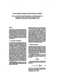
A representative power delivery network with on- chip power supplies, decoupling capacitors, and load circuits is illustrated in Fig. 1. A high power efficiency, ...
Distributed Power Network Co-Design with On-Chip Power Supplies and Decoupling Capacitors Selc¸uk K¨ose and Eby G. Friedman Department of Electrical and Computer Engineering University of Rochester Rochester, New York 14627 {kose,friedman}@ece.rochester.edu Abstract— With each technology generation, the power delivery network becomes larger and more complicated, making the system analysis process computationally complex. The rising number of on-chip power supplies and intentional decoupling capacitors inserted throughout an integrated circuit further complicates the analysis of the power distribution network. Interactions among the on-chip power supplies, decoupling capacitors, and load circuitry are investigated in this paper. The on-chip power supplies and decoupling capacitors within the power network are simultaneously co-designed and placed. The effect of physical distance on the power supply noise is investigated. This methodology changes conventional practices where the power distribution network is designed first, followed by the placement of the decoupling capacitors.
I. I NTRODUCTION With technology scaling, power supply voltages become lower, clock rates rise, and greater functionality is integrated on-chip, significantly increasing the power dissipation [1], [2]. Faster transition times and higher current demands produce larger voltage droop due to resistive IR and inductive L di/dt noise [3]. Due to the self- and mutual inductance of the power lines, the power grid impedance increases with frequency [1]. Lowering the target impedance of the power distribution network has therefore become increasingly important [4]. Multiple decoupling capacitors are placed on-chip to provide local charge to the load circuitry, effectively reducing the impedance between the power supplies and load circuits [5]. Multiple power supplies are widely used in high performance integrated circuits to provide current close to the load circuitry in high performance integrated circuits [6]. The number of on-chip power supplies is increasing, requiring innovative design methodologies to satisfy stringent noise and power constraints of these high complexity integrated circuits [1], [2]. Placing the power supply on-chip eliminates losses due to the parasitic impedances of the package , improving the quality of the delivered power [6]. To provide multiple on-chip power supplies, linear voltage regulators are typically used which require small area with fast load regulation to realize point-of-load voltage delivery [7]. These power supplies alone, however, do not satisfy stringent This research is supported in part by the National Science Foundation under Grant Nos. CCF-0811317 and CCF-0829915, grants from the New York State Office of Science, Technology and Academic Research to the Center for Advanced Technology in Electronic Imaging Systems, and by grants from Intel Corporation and Qualcomm Corporation.
power and noise constraints. Decoupling capacitors are therefore also widely used as a local reservoir of charge which are self activated and supply current when the power supply level deteriorates [8]. Inserting decoupling capacitors into the power distribution network is a natural way to lower the power grid impedance at high frequencies [4]. Tens of on-chip power supplies, hundreds-to-thousands of on-chip decoupling capacitors, and millions-to-billions of active transistors are anticipated in the design of next generation high performance integrated circuits [9]. A representative power delivery network with onchip power supplies, decoupling capacitors, and load circuits is illustrated in Fig. 1. A high power efficiency, global power supply provides the input voltage to the distributed ultrasmall voltage regulators. The regulators in each voltage island, with the local decoupling capacitors and power distribution network, deliver current to the local circuitry. Power supplies and decoupling capacitors exhibit similar characteristics with some important differences such as the response time, decay rate of the capacitor, on-chip area, and power efficiency. On-chip power supplies require greater area, provide limited power efficiency, and exhibit slower response time as compared to the decoupling capacitors [10]. Decoupling capacitors, however, should be placed close to a power supply to recharge before the next switching event [8]. Additionally, the placement of the decoupling capacitors should consider the resonance formed by the decoupling capacitor and the power grid inductance which degrades the effectiveness of the decoupling capacitor [11]. Existing design methodologies for placing decoupling capacitors assume one or two on-chip power supplies [8] or one decoupling capacitor interacting with multiple power supplies [12]. These assumptions are inappropriate when point-of-load voltage regulation is integrated with multiple on-chip power supplies and decoupling capacitors. Design methodologies are therefore required to simultaneously place multiple on-chip power supplies and decoupling capacitors. The effective radii of the decoupling capacitors have been developed for a single current path between a current load and a single decoupling capacitor in [8] and for a mesh structure considering a single decoupling capacitor in [12]. The interactions among the power supplies, decoupling capacitors, and load circuitry, schematically illustrated in Fig. 2, become more complicated with the increase in the number of components within the power delivery network. In this paper,
Decoupling capacitor
Point−of−load power supply Global power supply Fig. 1.
Distributed power supplies with decoupling capacitors utilizing an efficient on-chip buck converter and multiple ultra-small voltage regulators.
Vc
Power supply
1 0 I dl
Lvd
Decap
Ic
C
R dl
Decap Ldl
R vd Load
I vd
11 00 Vdd
I pl
Power supply
Fig. 2. Interactions among the on-chip power supplies, decoupling capacitors, and load circuitry. Thicker lines represent greater interaction. Note that the effect of a power supply or a decoupling capacitance on the load circuitry depends strongly on the physical distance.
interactions among the power supplies, decoupling capacitors, and current loads are investigated. A methodology is proposed to simultaneously determine the optimum location of the distributed power supplies and decoupling capacitors within the overall power distribution network, providing an integrated approach to delivering power. The rest of this paper is organized as follows. The problem is formulated in Section II. Interactions among the on-chip power supplies, decoupling capacitors, and load circuitry are analyzed and a methodology for simultaneous power supply and decoupling capacitor placement is presented in Section III. Case studies examining the interactions among the power supplies, current loads, and decoupling capacitors are provided in Section IV. Some specific conclusions are drawn in Section V. II. P ROBLEM F ORMULATION Power distribution networks are typically modeled as a uniformly distributed RL mesh structure. By exploiting the uniform nature of the power grid, the euclidean distance between the circuit components can be used to determine the effective impedance between arbitrary nodes. A closed-form expression for the effective impedance in an infinite resistive
1 0 Vload
R pl
Lpl
Load
Il
Imax tr
tf
Fig. 3. Simplified interactions among a power supply, decoupling capacitor, and load circuit. The components are connected with the corresponding equivalent impedance in the power grid modeled by (1). The load current is modeled as a triangular current load with a rise time tr and fall time tf .
mesh is provided by Venezian in [13]. This expression is slightly modified to include the inductance of the power grid as the power grid impedance depends strongly on the inductance at high frequencies. A closed-form expression to determine the effective impedance between two nodes, Nx1 ,y1 and Nx2 ,y2 , is Zm,n = z ∗
1 ∗ ln(n2 + m2 ) + 0.51469, 2π
(1)
where m = |x1 − x2 | and n = |y1 − y2 |.
(2)
z is the impedance of one segment of the grid. Applying this effective impedance concept, multiple current paths are considered without increasing the computational complexity of the power grid analysis process. The complex power distribution network schematically illustrated in Fig. 2 is simplified to a network consisting of only equivalent impedances among the power supplies, decoupling capacitors, and load circuitry. Multiple current paths are efficiently considered using the simplified model described by (1).
III. S IMULTANEOUS P LACEMENT OF P OWER S UPPLIES AND D ECOUPLING C APACITORS The interactions among a single power supply, decoupling capacitor, and current load are illustrated in Fig. 3. The equivalent parasitic resistance and inductance between the power supply and decoupling capacitor, power supply and load circuit, and decoupling capacitor and load circuit are represented, respectively, as Rvd and Lvd , Rpl and Lpl , and Rdl and Ldl . The load current Il is Il = idl + ipl .
(3)
The current supplied from the decoupling capacitor and power supply is represented, respectively, as idl and ipl . The ratio of the current supplied to the active circuits from the power supplies and decoupling capacitors depends upon the physical distances, the parasitic impedance among these components, and the size of the decoupling capacitors. idl /il increases for greater Rpl and Lpl , enhancing the effect of the decoupling capacitors on the load circuit as compared to the effect of the power supplies on the load circuit. The effective region of a decoupling capacitor depends upon the location of those power supplies, decoupling capacitors, and load circuits in close proximity as well as the power grid impedance, and the transition time of the load currents. A uniform current distribution is assumed in this paper to simplify this analysis. The analysis can however be generalized to a non-uniform load current distribution. The effective region for a single decoupling capacitor with a single power supply is illustrated in Fig. 4. The effective region is not a uniform circle as previously proposed in [8], [12], but exhibits an elliptic shape due to the non-uniform location of the power supplies. This elliptic shape can be explained intuitively by examining Fig. 4. The current supplied to the load circuit in this elliptic region is provided by the decoupling capacitor and the local power supply. When the load circuit is no longer within this elliptic region, most of the load current is provided either by the local power supply or decoupling capacitor due to the increased parasitic impedance of the interconnect connecting the load to the source of charge. When the load current is supplied both by the local power supply and the decoupling capacitor, the response is faster and more effectively suppresses the switching noise. The elliptic shape also depends upon the technology parameters and the noise constraints. The area of the elliptic region is small when the noise constraints of the power distribution network are high. For example, when the maximum target noise of the power distribution system is 5% of the supply voltage, a smaller ellipse is formed as the effective region around the decoupling capacitor. Alternatively, the area of the elliptic region increases when the noise constraint is increased to 10% of the supply voltage. Consequently, elliptic equipotential shapes are formed around the decoupling capacitors and power supplies, denoting identical power supply voltage levels. An elliptic region is described by a long and short radius represented, respectively, as rl and rs as shown in Fig. 4. rl
Maximum target noise 15% 10% 5%
Decoupling capacitor effective region
z rs
rl Decoupling capacitor
Power supply
Fig. 4. Elliptic structure to illustrate the effective region of a decoupling capacitors with a single power supply. The short radius (rs ) and long radius (rl ) depend upon the size of the capacitor and the effective impedance between the capacitor and power supply. Note that the effective region is greater when the maximum tolerable noise target increases.
can be determined as rl(n,m) =
K ∗C , R(m,n) + k ∗ L(m,n)
(4)
where C is the decoupling capacitance and the effective resistance and inductance between the decoupling capacitor and the power supply are represented, respectively, as R(m,n) and L(m,n) . The horizontal and vertical distance from the decoupling capacitor to the power supply is represented, respectively, as m and n. The effect of the transition time of the load current is embedded into the equation using k. K models the noise constraints, i.e., a smaller K is used for more stringent noise constrained circuits. For instance, a greater K is chosen for a maximum noise target of 15% as compared to a maximum tolerable noise target of 10% or 5% (see Fig. 4). The resulting rl is greater for the 15% maximum tolerable noise target, as illustrated in Fig. 4. rs is also determined utilizing the transition time of the load current, the distance between the decoupling capacitor and the power supply, and the size of the capacitor, similar to rl . The effective region for a local power supply with four decoupling capacitors is illustrated with a dark shaded modified elliptic shape in Fig. 5. Since the power supply interacts with four different decoupling capacitors, the effective region is the overlap of the four different elliptic shapes. Since the effect of a decoupling capacitor on rs is limited, the effective region of the power supply can be described with four different rl , denoted as rl1 , rl2 , rl3 , and rl4 , to represent, respectively, the effect of C1 , C2 , C3 , and C4 . A similar analysis can be performed when the system includes multiple decoupling capacitors and multiple power supplies. Each decoupling capacitor is affected by the remaining decoupling capacitors and power supplies. The effective region of a decoupling capacitor or power supply can therefore be described as the overlap of the elliptic equipotential surfaces caused by each power supply and decoupling capacitor, as illustrated in Fig 5. IV. C ASE S TUDY The proposed method of overlapping elliptic equipotential surfaces to determine the effective region has been verified with SPICE simulations. A uniform RL grid structure with 20
C4 effective region Local power supply effective region C1 effective region
C4
18
C
2
16
Local power supply
0.961
z4
14
C1
z1 rl
20
C1
12
0.953 0.945
r
l2
0.937
0.953 0.961 0.945 0.992 0.953 0.937
10
0.929
8
4
rl
z2 Vdd
z3 rl
C3
6
1
4
rl
2
3
C2
C3 C2 effective region C3 effective region
Fig. 5. Modified elliptic structure to illustrate the effective region for a local power supply and decoupling capacitors. Note that the effective region for a local power supply is the overlap of the effective region of the surrounding decoupling capacitors.
horizontal and vertical lines (a 20 x 20 mesh) is assumed in the analysis. The supply voltage is 1 volt and the uniformly distributed current loads switch at a 1 GHz frequency with rise and fall times of 100 ps and 300 ps, respectively. A power distribution system with a local power supply and four decoupling capacitors is initially considered. The power supply is placed at N(10,10) and the decoupling capacitors C1 , C2 , C3 , and C4 are placed, respectively, at nodes N(6,14) , N(17,17) , N(5,5) , and N(18,2) . A simulation of the power distribution network is illustrated in Fig. 6. Since the closest decoupling capacitor to the local power supply is C1 , the effective region of the power supply extends towards C1 . Alternatively, the effective region of the local power supply is limited towards C4 since C4 is farther from the local power supply. The long radius of the effective region for C2 and C4 is shown in Fig. 6, respectively, as rl2 and rl4 . The ratio rl2 /rl4 is 1.2 as compared to 1.15 from (4), exhibiting an error of less than 5%. The ratio rl2 /rl4 is used for a comparison since an error parameter is easier to incorporate within the proposed model by comparing the ratios. The effect of the transition time of the load current on the effectiveness of the decoupling capacitors and power supplies has also been investigated. A 20 x 20 power grid with five decoupling capacitors placed at N(3,3) , N(3,17) , N(10,10) , N(17,3) , and N(17,17) and four on-chip power supplies located at N(3,10) , N(10,3) , N(10,17) , and N(16,10) is evaluated. For rise and fall times of the load current of 50 ps and 150 ps, respectively, the effective region for the decoupling capacitors and power supplies is illustrated in Fig. 7a. Note that the effective region of the power supplies and decoupling capacitors exhibits a similar elliptic shape. No resonance occurs and the decoupling capacitors are sufficiently close to the power supplies to be recharged before the next switching event. The effective region of the power supplies and decoupling capacitors is depicted in Fig. 7b when the rise and fall
0 0
rl4
0.929 0.937
2 2
4
6
8
10
12
14
C4 16
18
20
Fig. 6. Effective region for a local power supply at N(10,10) with four decoupling capacitors at N(17,17) , N(18,2) , N(5,5) , and N(6,14) . Note the elliptic shapes around the decoupling capacitors and modified elliptic shape around the local power supply.
transition times of the load current are increased, respectively, to 200 ps and 600 ps. Note that the area of the effective region of the decoupling capacitors becomes smaller. The cause of the reduced effective region around the decoupling capacitors is that the equivalent transition times produce a resonance [11] formed by the decoupling capacitor and the power grid inductance. Also, note that the capacitors cannot fully recover before the next switching event. The resonance phenomenon is considered in (4) with k. The effective region around the on-chip power supplies is not significantly affected by the change in transition time. Considering all of these distinct properties of the decoupling capacitors and power supplies (such as resonance and the decay rate of the capacitor) can significantly improve the quality of the power delivery process.
V. C ONCLUSIONS A change in the design process of power distribution networks is necessary with the increase in the number of on-chip power supplies. This paper addresses the analysis and simultaneous co-placement of on-chip power supplies and decoupling capacitors in high performance integrated circuits. The effectiveness of a decoupling capacitor depends strongly on the distance between that decoupling capacitor and the neighboring on-chip power supplies. A closed-form expression is provided to determine the effective impedance between two nodes in a uniform RL power distribution network. The effective region for decoupling capacitors and power supplies exhibits an elliptic shape. A closed-form expression to determine the long radius of this elliptic shape is also provided. The error of this closed-form expression as compared to SPICE is less than 5%. The validity of the proposed method of overlapping equipotential elliptic surfaces is verified with SPICE. The effective region of the decoupling capacitors is significantly affected by the transition time of the load current due to the resonance formed by the power grid inductance and decoupling capacitors.
20
C
C
V
1
18
2
1
16 14
C
3
V
12
2
0.925
10 8
0.92 0.914
6
0.909
C
4
0.884
V3
0.955
0.974 0.899 0.894
0.904
C
V4
4
5
2 0 0
2
4
6
8
10
12
14
16
18
20
a) 20
C
C2
V
1
18
1
16 14 12
C3
V2
0.941 0.945
0.932
0.974
10 0.936
8
V
0.941 0.936
3
6 0.932 4 2 0 0
0.928
V4 2
4
0.92 0.916
C5
C4 6
8
10
12
14
16
18
20
b)
Fig. 7. Effective region for multiple decoupling capacitors and power supplies. Four decoupling capacitors, C1 , C2 , C4 , and C5 , are located at the corners and one decoupling capacitor C3 is located in the middle of the power distribution network. The four power supplies are placed between the decoupling capacitors. The rise and fall transition times are, respectively, a) 50 ps and 150 ps, and b) 200 ps and 600 ps.
R EFERENCES [1] R. Jakushokas, M. Popovich, A. V. Mezhiba, S. Kose, and E. G. Friedman, Power Distribution Networks with On-Chip Decoupling Capacitors, Second Edition, Springer, 2011. [2] S. Pant, D. Blaauw, and E. Chiprout, “Power Grid Physics and Implications for CAD,” IEEE Design and Test of Computers, Vol. 24, No. 3, pp. 246–254, May 2007. [3] P. Larsson, “di/dt Noise in CMOS Integrated Circuits,” Analog Integrated Circuits and Signal Processing, Vol. 14, No. 2, pp. 113–129, September 1997. [4] L. Smith et al., “Power Distribution System Design Methodology and Capacitor Selection for Modern CMOS Technology,” IEEE Transactions on Advanced Packaging, Vol. 22, No. 3, pp. 284–291, August 1999. [5] H. H. Chen and S. E. Schuster, “On-Chip Decoupling Capacitor Optimization for High-Performance VLSI Design,” Proceedings of the IEEE International Symposium on VLSI Technology, pp. 99–103, May/June 1995. [6] V. Kursun and E. G. Friedman, Multi-Voltage CMOS Circuit Design, Wiley & Sons, 2006. [7] P. Hazucha et al., “Area-Efficient Linear Regulator with Ultra-Fast Load Regulation,” IEEE Journal of Solid-State Circuits, Vol. 40, No. 4, pp. 933–940, April 2005. [8] M. Popovich, M. Sotman, A. Kolodny, and E. G. Friedman, “Effective Radii of On-Chip Decoupling Capacitors,” IEEE Transactions on Very Large Scale Integration (VLSI) Systems, Vol. 16, No. 7, pp. 894-907, July 2008. [9] B. Amelifard and M. Pedram, “Area-Efficient Linear Regulator with Ultra-Fast Load Regulation,” IEEE Transactions on Computer-Aided Design of Integrated Circuits and Systems, Vol. 28, No. 6, pp. 888–900, June 2009. [10] W. Kim, M. S. Gupta, G.-Y. Wei, and D. Brooks, “System Level Analysis of Fast, Per-Core DVFS Using On-Chip Switching Regulators,” Proceedings of the IEEE International Symposium on High Performance Computer Architecture, pp. 123–134, February 2008.
[11] E. Salman, E. G. Friedman, R. M. Secerenau, and O. L. Martin, “Worst Case Power/Ground Noise Estimation Using an Equivalent Transition Time for Resonance,” IEEE Transactions on Very Large Scale Integration (VLSI) Systems, Vol. 56, No. 5, pp. 997–1004, May 2009. [12] A. Todri, M. Marek–Sadowska, F. Maire, and C. Matheron, “A Study of Decoupling Capacitor Effectiveness in Power and Ground Grid Networks,” Proceedings of the IEEE International Symposium on Quality Electronic Design, pp. 653–658, March 2009. [13] G. Venezian, “On the Resistance between Two Points on a Grid,” American Journal of Physics, Vol. 62, No. 11, pp. 1000–1004, November 1994.