International Journal of Scientific & Engineering Research Volume 2, Issue 10, Oct-2011 ISSN 2229-5518
1
Dynamic Response of Jospephson Resistive Logic (JAWS) GATE K.Srinivas and J. C. Biswas
ABSTRACT---In this paper a thorough investigation of resistive logic gate, JAWS (Josephson Auto-Weber System) has been made. The current equations of this gate at each stage have been deduced. The dynamic response of this gate has been obtained by the computer-simulation. Our concept of turn-on delay of Josephson junction has been introduced. The effect of overdrive current on turn-on delay for JAWS resistive logic gate has been shown. This will provide a better understanding of switching dynamics of the JAWS logic gate. Further, we have shown the effect of overdrive current on this logic gate.
—————————— ——————————
INTRODUCTION
T
wo attractive features of SQUID devices for logic applications are isolation and serially connected fan-out. The isolation is provided by the transformer coupling between the SQUID and the input. The isolation is not perfect in the sense that a noise pulse (typically 5 percent) is fed back into the control line when the SQUID switches to the non-zero voltage. The other advantage is the serial fan-out capability by which the control lines of many load devices can be connected in series with a single output line. The main drawbacks of SQUID devices for logic application are relatively large device area and high sensitivity to stray magnetic fields. In SQUID 80% of the area is occupied by the transformer [1]. Further, the high sensitivity to stray magnetic field requires that the SQUID based logic circuits be well shielded from the stray magnetic fields. The resistive logic gates such as JAWS (Josephson Auto-Weber System) [2], DCI (Direct Coupled Isolation) [3] and RCJL (Resistor Coupled Josephson Logic) [4] are chosen because the gate logic delay in this case would consist of the turn-on delay, switching delay and propagation delay, but not the crossing delay as in the case of magnetically coupled logic gates. Further, these resistive logic gates do not have a factor of limiting the size very seriously. So, the gate propagation delay can be made sufficiently small. Therefore, the small time constant of the Josephson junction can be directly attained to these gates. It has been considered by the earlier workers [5] that the turn-on delay of a logic gate is the time taken for the logic gate to obtain 2% of the output current to the load. This consideration seems to be orbitrary. DEPARTMWENT OF PHYSICS, GMR INSTITUTE OF TECHNOLOGY, RAJAM-532127,A.P., INDI,A Email :
[email protected] [email protected] DEPARTMENT OF ELECTRONICS AND ELECTRICAL COMMUNICATION ENGINEERING, INDIAN INSTITUTE OF TECHNOLOGY , KHARAGPUR-721302 INDIA.
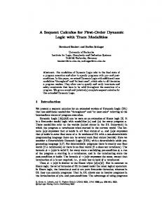
Due to this fact, in the present paper we have made a thorough investigation of the resistive logic gate JAWS. Our concept of turn-on delay[6] has been introduced which will be able to remove the confusion in critically ascertaining the switching speed of these logic gates. Further, the effect of overdrive current on these resistive logic gates has been studied. JAWS (Josephson Auto-Weber system A gate of this kind has been reported by Fulton, et al [2] and is called JAWS. The basic gate employs two junctions and a resistor as shown in Fig.1 where J1 and J2 represent Josephson junctions with critical currents 2Io and Io and junction capacitances 2Cj and Cj respectively. RL is the load resistor with a resistance rL. R is the input resistor with a resistance r The JAWS gate is biased in the superconducting state by the gate current Ig and the offset current Ioff. The current levels in J1 and J2 are Ig -Ioff and Ioff, respectively. When the input signal Iin is directly injected to this JAWS device, it will add to the bias current in junction J1 and subtract from the bias current in junction J2. The junction J1 is a current-summing junction which switches first in the gate. This makes J1 highly resistive, steering most of the signal and the gate current leads to ground through the resistor R. The gate current Ig is selected to be sufficient to then switch J2 to the non-zero voltage state. With both J1 and J2 in the high-resistance state, the gate current is steered to the load R and the signal current to ground via the resistor R. The high-resistance of J2 prevents gate current from feeding back into the input signal line and thus provides isolation. However, the isolation is not perfect and a small amount of current (typically 5%) is fed back into the input line.
IJSER © 2011 http://www.ijser.org
International Journal of Scientific & Engineering Research Volume 2, Issue 10, Oct-2011 ISSN 2229-5518
In Fig.2 we have shown the current equations at
2
i 4 V a / rL
each stage of the logic gate mentioned. According to Fig.2, the current equation at each stage can be
Va
written as:
(4)
o d a d b , Vb o 2 dt 2 dt
I g i1 i2 i 4 and
(5) (6)
I in i2 ioff i3
(7)
(Note: Here the effect of subgap quasiparticle resistance Rj has been neglected since Rj >>r, r, ). a) Static case:
Va Vb 0
d b 0 i3 i4 0 dt
After using the above conditions Eqns.(1) and Fig. 1 Circuit configuration of the resistive logic
(2) lead to
Ig
gate JAWS with threshold characteristics.
Io
2 sin a
I off Io
I in Io
(I)
Eqn.(I) describes the static behaviour of the JAWS gate. A static curve between Ig/Io and Iin/Io will give the operating margins and gain margins of the JAWS gate. b) Dynamic case: Eqn. (1) can be written as
i1 2 I o sin a 2 C j
Fig. 2 Circuit configuration of the resistive logic gate JAWS with current indication at each stage of the logic gate.
i1 2 I o sin a 2 C j
dVa dt
i 2 I o sin ( a b ) C j i3 Vb / r
d 2 a I o dt 2 2
d 2 a or [ i1 2 I o sin a ] 2 o C j dt
(8)
Similarly, Eqn.(2) can be written as
d 2 b i 2 [ 1 i2 2 o C j 2 dt 2 I o sin a I o sin ( a b ) ]
(1)
d (V a Vb ) dt (2) (3)
Further, from Eqns. (6) and (7) we get,
i1 I g I in I off (i3 i4 ) i2 I off I in i3
IJSER © 2011 http://www.ijser.org
(9)
International Journal of Scientific & Engineering Research Volume 2, Issue 10, Oct-2011 ISSN 2229-5518
Substituting the above values i1 and i2 in Eqns.(8) and(9), we obtain,
3
we have adopted in the present case in order to investigate the switching dynamics of logic gates.
d 2 a [ i g I in I off 2 I o 2 o C j dt sin a
o d b o d a ] 2 r dt 2 rL dt
(II)
and
ig 3 d 2 b 2 [ I in 2 o C j 2 2 dt
3 I off 2 I o sin a I o sin ( a b ) 2
3 o d b o d a ] 4 r dt 4 rL dt
(III) Computer-simulated pulse response of the JAWS gate can be obtained by solving the Eqns.(II) and
(III)
for
an
input
current
Iin applied as a step function at t=0 with amplitude 1.5 Ith (threshold current). To solve these equations the initial conditions for
a( ao)
and
b(
bo)are to be known which can be deduced as follows: At t = 0, From Egns. (6) and (7)
I i1 i2 and i 2 ioff
or ao sin 1 (
I g I off 2 Io
) (a)
and 1
bo sin (
I g I off 2 Io
) sin
1
(
I off Io
) (b)
In Fig.3 the current variations with time at different stages of the JAWS gate (shown in Fig.2) have been plotted. The parameters chosen for plotting are Io = 0.1mA and Cj = 0.8pF. These curves are almost similar to those obtained by Josephson [5] using computer simulation. This gives confidence to our simulation approach that
Fig. 3 Simulated switching dynamics of the JAWS gate. Circuit parameters used in the simulation are Io = 0.1 mA, Cj = 0.8 pF, r = 0.8 , rL = 10 . Since Nb/Al0 x/Nb Josephson technology has better qualities over Pb-alloy technology, we have used Nb/A10 x/Nb Josephson junction parameters for the simulation of the resistive logic gate JAWS. The parameters used are Io = 87mA and Cj = 0.37pF. It may be pointed out that in estimating the turn-on delay of a logic gate, Sone [5] has considered the time that is needed to reach 2% of the output current to the load. This consideration seems to be arbitrary. In the present case we have defined turn-on delay of a logic gate in a more critical way using the concept of the turn-on delay of Josephson junction discussed in Srinivas [6]. It is the time taken by the output phase to reach to a value /2. It is expected that this definition will be able to remove confusions in defining the turn-on delay of a logic gate. The dynamic response of a JAWS gate at each stage have been drawn in Fig.4 using Nb/A10 x/Nb Josephson technology. The solid curve indicates the current variation (i3) with time at stage 'b' as shown in Fig.2 and the dotted curve indicates the current i4 (output current) with time at a stage 'A'. It can be observed from Fig.4 that the output current i4 has come more quickly to its saturation value than in Fig.3. This is due to the low junction capacitance value that has been considered in the former case. In Fig.5 we have
IJSER © 2011 http://www.ijser.org
International Journal of Scientific & Engineering Research Volume 2, Issue 10, Oct-2011 ISSN 2229-5518
4
shown the simulated switching dynamics of the JAWS gate when the subgap resistance is taken
0.75I0.
into consideration. Fig. 4 Simulated switching dynamics of the JAWS gate. Circuit parameters used in the simulation are from Nb/A10x/Nb Josephson technology and are given as Io = 0.087 mA, Cj = 0.37 pF, r = 0.8 , rL = 10 . The switching waveforms i3 and iout are simulated waveforms of current flowing in the input resistor R and the output current respectively.
Fig. 6 Simulated phase evolution vs time for a JAWS gate. a and a - b are the phase differences of the junmctions J1 and J2, respectively. Circuit parameters used in the simulaton are Io = 0.087 mA, Cj = 0.37 pF, r = 0.8 and rL = 10 . Using our concept of turn-on delay (discussed above), the turn-on delay at each stage of the JAWS gate has been indicated. This will give an exact physical understanding of switching dynamics of the JAWS gate. Also we have plotted (Fig-7a and Fig.7b) the effect of overdrive current on the turn-on delay of a JAWS gate under different biasng conditions, Ig = 0.75 Io, 1.5 Io and 2.25 Io. In Fig.7a the solid curve shows the TD variation of stage with overdrive and the dotted curve indicates the TD variation of 'b' stage with overdrive. It can be observed from Fig.7 that the turn-on delay of a JAWS gate decreases with the increase of overdrive current. Also, the turn-on delay decreases with the
Fig. 5 Simulated switching dynamics of the JAWS gate when the subgap resistanes are taken into consideration. Further, in Fig.6 we have shown the phase variations with time at different stages of the JAWS gate. The biasing and overdrive current conditions are as follows: Ig = 1.5 Io ; Iin =1.5 Io and Ioff=
Fig. 7a Turn-on delay of the JAWS gate vs input
IJSER © 2011 http://www.ijser.org
International Journal of Scientific & Engineering Research Volume 2, Issue 10, Oct-2011 ISSN 2229-5518
current. IDa and IDb represent the turn-on delay veriation with time at point ‘a’ and ‘b’ respectively (as shown in Fig 2)
Fig 7b. Turn-on delay of the JAWS gate vs input current. IDa represent the turn-on delay variation with time at point ‘a’ and ‘b’respectively (as shown in Fig. 2).
5
current switched Josephson logic," Appl. Phys. Lett. . vol.34, no.10, May 1979, pp. 709711. [3] T. R. Gheewala and A. Mukherjee, " Josephson direct coupled logic (DCL)," IEDM Tech. Dig., (Washington DC, December 3-5, 1979), pp. 482-484. [4] J. Sone, T. Yoshida and H. Abe, " Resistor coupled Josephson logic," Appl. Phys. Lett. vol.40, 1982, p.741. [5] J. Sone, " Turn-on delay analysis of currentinjection Josephson circuits," J. Appl. Phys. vol.57, no.ll, June 1985, pp. 5028-5034. [6] K. Srinivas, J. C. Biswas , " Turn-on delay of a Josephson junction," J of Low Tempererature Physics” , vol.74, Nos. 5/6 1989 , pp.407-415. [7] K. Srinivas, J. C. Biswas, “ Dynamic response of Josephson resistive logic ( DCI) gate “ , ICCDC-11, THAI (SUBMITTED) [8] K. Srinivas, J. C. Biswas, “ Dynamic response of Josephson resistive logic ( RCJL) gate “ , ICECS-11, INDONESIA (SUBMITTED)
increase of biasing rate. So by choosing large biasing and overdrive currents we can minimize the turn-on delay of the JAWS gate. In a similar manner a thotough investigation of other resistive logic gates, DCI logic gate [7} and RCJL gate[8] have been made which gives better understanding of logic gates before they could be fabricated experimentally.
CONCLUSIONS A thorough investigation of JAWS logic gate has been made . The dynamic response of this logic gate has been obtained by computer-simulation. The concept of our turn-on delay has been introduced which has helped us in critically ascertaining the switching speed of the logic gate. The effect of turn-on delay on overdrive current has been studied. It is observed that for low fanouts, the JAWS logic gate seems to be a better choice for Josephson logic circuit application. It is expected that the concept of turn-on delay will be able to remove confusions which are lying in the earlier investigations.
REFERENCES [1] T. R. Gheewala, " Josephson logic devices and circuits," IEEE Trans. Electron Devices vol.ED-27, no.10, October 1980, pp.18571869. [2] T. A. Fulton, S. S. Pei and L. N. Dunkleberger, " A simple high performance IJSER © 2011 http://www.ijser.org