Dynamical System Guided Mapping of Quantitative Neuronal Models ...
Recommend Documents
ized set of basic models of ASM1 [11], ASM2 [12] and ASM3 [9, 13], and they have been widely accepted in scientific fields but still have some weaknesses in ...
2004 Society for Chaos Theory in Psychology & Life Sciences. Dynamical ...
equations describing the time-variation of the love or hate displayed by
individuals ...
Abstract. An approach called growth model-based mapping (GMM) of quantitative trait loci (QTLs) is proposed in this paper. The principle of the approach is to fit ...
May 21, 2002 - M. Spears, Morgan Kaufmann, 2001, pp. .... of the element i is described by a heuristic function G. (For a genetic algorithm, G will describe ...
Orsatti, and J. R. C. Piqueira, IEEE Trans. Neural Netw. 14,. 1572 2003. 64 L. H. A. Monteiro, M. A. Bussab, and J. G. Chaui-Berlinck, J. Theor. Biol. 219, 83 2002.
Bernard Choi,2 and Bruce J. Tromberg2,*. 1Department of Physics, 4129 ..... D. J. Pine, D. A. Weitz, P. M. Chaikin, and E. Herbolzheimer,. âDiffusing wave ...
frequency domain imaging, a technique where samples are illuminated with sinusoidal intensity patterns of light that control ..... was obtained from the Oregon Medical Laser Center website. [29]. ..... methods, such as rapid-find lookup tables.
values of the Î. It is just what is called the cosmological constant problem requiring ... In this context an idea of a running cosmological constant term appears.
tion systems at signalized intersections, including detection design .... tally, camera height, detector length and width, and vehicle dimension. Tian and Abbas. 51.
Fault Tree Modeling. 2. Quantitative analysis of imprecise system models with configurable fault trees. Spring Meeting 2016 in Graz. RAID. Controller. Failure.
Nov 12, 2013 - Proteins exist as inter-converting conformational states under ambient conditions ...... (TIFF). Figure S11. The contacts between K120 of DNA-free DBD .... (2002) The. IARC TP53 database: new online mutation analysis and.
a to e, X 48,000. b' and d', 10â tilt, X 75.000. Figure 9. Diagram summarizing endomembrane relationships among. RER elements and the Golgi apparatus.
Jul 30, 2015 - Abstract: Flat EEG is a way of viewing electroencephalography signals on the real plane. The wealth of information contained within makes it a ...
Invasive Mapping Guided Surgical Treatment of Atrial Fibrillation. Utopia or Near Future? ... Gaita et al reported a success percentage of only 25% after complete ...
World Health Organization's (WHO) data shows that most cases of TB are .... projects in Thailand from 1960 to 1963 were used to estimate the parameters incorporated ... to the pool of new infected, namely, some individuals would move from the suscept
tailed review of the work carried out mostly by the authors and col- laborators ... Tuberculosis (TB) is a disease that affects human and animal population. .... Finally a list of challenges ... function to model infection rates in the implementation
2.4D, upper panel). Interestingly, for the ... 2.4E) to examine how the four drug conditions can modulate spike properties. ...... Dastoor D, Ervin F, Gauthier L, et al.
May 31, 2016 - tive evaluation of 3D saliency models, making it impossible to ob-. arXiv:1605.09451v1 [cs. ... performance using raw saliency maps. In contrast, there are well- ..... cluding C++, Matlab and Python. Results show, in Section ...
development. Our aim is that students learn the fundamental skills to construct correct, robust, reuseable and extensible software systems. Some preliminary ...
Department of BioMedical InfoPhysics, Science Research Inst., 205 Hana Road, Edison NJ 08817, .... velocity vi of Ïi; Ei, Hi, Ïi and vi are functions of spatial.
Aug 7, 2009 - papers proposing neuronal network models of different complexity and ...... Küppers G, Lenhard J (2005) Validation of simulation: Patterns in the social and ... Le Nove`re N, Finney A, Hucka M, Bhalla US, Campagne F, et al.
Feb 1, 2008 - We explicitly show that in quintessence-type models the dark energy fluctuations, ..... sound speed of the dark energy fluid is significant, then.
Dynamical System Guided Mapping of Quantitative Neuronal Models ...
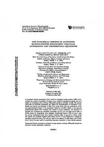
present study, we first calibrate the on-chip bias generators on our custom hardware. Then ... B. V. Benjamin is with the Department of Electrical Engineering, Stanford. University, Stanford ... Quadratic IF Neuron with = 30 ms. (a) The dynamical ...
This article has been accepted for inclusion in a future issue of this journal. Content is final as presented, with the exception of pagination. IEEE TRANSACTIONS ON CIRCUITS AND SYSTEMS—I: REGULAR PAPERS, VOL. 59, NO. 11, NOVEMBER 2012
1
Dynamical System Guided Mapping of Quantitative Neuronal Models Onto Neuromorphic Hardware Peiran Gao, Ben V. Benjamin, and Kwabena Boahen, Member, IEEE
Abstract—We present an approach to map neuronal models onto neuromorphic hardware using mathematical insights from dynamical system theory. Quantitatively accurate mappings are important for neuromorphic systems to both leverage and extend existing theoretical and numerical cortical modeling results. In the present study, we first calibrate the on-chip bias generators on our custom hardware. Then, taking advantage of the hardware’s highthroughput spike communication, we rapidly estimate key mapping parameters with a set of linear relationships for static inputs derived from dynamical system theory. We apply this mapping procedure to three different chips, and show close matching to the neuronal model and between chips—the Jenson–Shannon divergence was reduced to at least one tenth that of the shuffled control. We confirm that our mapping procedure generalizes to dynamic inputs: Silicon neurons match spike timings of a simulated neuron with a standard deviation of 3.4% of the average inter-spike interval. Index Terms—Dynamical systems, neural simulation, neuromorphic engineering, quadratic integrate-and-fire model, silicon neuron.
I. QUANTITATIVE NEUROMORPHIC MAPPING EUROMORPHIC engineering aims to emulate computations carried out in the nervous system by mimicking neurons and their inter-connectivity in VLSI hardware [1]. Having succeeded in morphing visual [2], [3] and auditory [4], [5] systems into mixed-analog-digital circuits, engineers are entering the arena of cortical modeling [6]–[9]. This is an arena in which neuromorphic systems’ parallel operation and low energy consumption give them distinct advantages over software simulation. Reproducing existing theoretical and numerical cortical modeling results using the neuromorphic approach will be facilitated by establishing quantitative links between parameters of neural models and those of their electronic analogs. Furthermore, this will build a foundation for engineers to scale up neuromorphic models beyond the limit of software simulators. Initial attempts to map neural models onto neuromorphic chips took a model-less approach [Fig. 1(a)]. Key operating voltages or currents, and occasionally their transients, were measured using on-chip analog-to-digital converters or external
N
Manuscript received November 04, 2011; revised December 17, 2011; accepted January 23, 2012. This work was supported by the National Institute of Health (NIH) under Director’s Pioneer Award DPI-OD000965. This paper was recommended by Associate Editor V. Gaudet. P. Gao and K. Boahen are with the Department of Bioengineering, Stanford University, Stanford, CA 94305 USA (e-mail: [email protected]; [email protected]). B. V. Benjamin is with the Department of Electrical Engineering, Stanford University, Stanford, CA 94305 USA (e-mail: [email protected]). Digital Object Identifier 10.1109/TCSI.2012.2188956
Fig. 1. Approaches to quantitative neuromorphic mapping. Our approach is highlighted in bold. (a) Adjust circuit biases with heuristics to achieve the desired behavior without a model. (b) Use model simulation as reference to nonlinearly optimize the circuit’s behavior. (c) Mathematically analyze the model to derive a set of simple linear parametric relations.
instruments. These measurements were compared with the desired behavior, and circuit biases were adjusted using intuition or heuristic algorithms until the matching was acceptable [10], [11]. While such procedures capture the hardware operation in detail, they are time-consuming in both data collection and analysis, and space-consuming in terms of hardware, as special circuits have to be included to expose relevant circuit nodes. Recent successes in the application of dynamical system theory to computational neuroscience [12] make it now possible to take a model-guided approach to mapping neural models onto neuromorphic hardware. Instead of designing circuits to produce desired behaviors in an ad hoc fashion, designers synthesize current-mode subthreshold CMOS circuits directly from ordinary differential equations that govern the model’s state variables’ evolution, representing these state variables as currents [13]–[15]. This design procedure yields combinations of circuit biases that are mathematically related to neural model parameters through sets of hardware specific mapping parameters. Once these mapping parameters are determined, translating neuronal parameters into circuit parameters is straightforward. As many neuronal models exhibit complex dynamics, without simple analytical solutions, mapping parameters have so far been extracted through nonlinear optimization, using the model’s numerical simulation as a reference [Fig. 1(b)]. In one approach, the mapping parameters are adjusted iteratively until the circuit’s operating currents converge with the numerical simulation’s state variables. This iterative optimization procedure compensates for hardware discrepancies, starting with an initial set of biases computed from the circuit’s nominal mapping parameters (i.e., obtained from design specifications) [16], [17]. In another approach, the circuit behavior is approximately
This article has been accepted for inclusion in a future issue of this journal. Content is final as presented, with the exception of pagination. 2
IEEE TRANSACTIONS ON CIRCUITS AND SYSTEMS—I: REGULAR PAPERS, VOL. 59, NO. 11, NOVEMBER 2012
thousands of silicon neurons on three different chips from our custom hardware, Neurogrid, proposed in [9]. In Section II, we analyze the quadratic IF neuron model and its implementation in neuromorphic hardware. In Section III, we present the neuron circuit’s bias generator, and argue that its proper calibration is essential for accurate mapping. In Section IV, we apply the high-throughput, spike-based mapping procedure; and we demonstrate its accuracy and performance across different chips in Section V. Finally, in Section VI, we summarize our findings, and propose the procedure’s extension to other neuromorphic circuits such as adaptive, synaptic and ion-channel circuits.
II. SILICON NEURON
= 30
Fig. 2. Quadratic IF Neuron with ms. (a) The dynamical system’s phase portraits in the sub- and supra-threshold regimes, and at bifurcation 0, 1 and 0.5). Dark and empty circles indicate stable and unstable fixed (v points, respectively. Arrows indicate attracting or repelling directions. At the bifurcation point (0.5), the saddle point attracts from below and repels from above. (b) Tonic spiking rate with supra-threshold drives. The neuron starts spiking at the bifurcation point. (c) Example v t traces with subthreshold . There is a stable fixed point at v drive v and an unstable fixed . (d) Example v t traces with supra-threshold drive v . point at v In the absence of any fixed points, the neuron spikes repeatedly.
= (
= 0) =2
()
() =0
The quadratic IF neuron uses a quadratic positive feedback term to model the dynamics of voltage-gated sodium channels [20]; it has become the model of choice for large software simulations [21]. We analyze its bifurcation and spiking rate using dynamical system theory, and show how to match these dynamics in silicon.
( = 1)
fitted by a simpler intermediate model. Then, the intermediate model’s parameters are related to those of the neuronal model through nonlinear optimization of these two models’ simulation results [18]. However, these approaches are time-consuming, and have been restricted to only tens of neurons and their performance has not been demonstrated across multiple chips. While the complexity of neuron models as a whole seems to merit the nonlinear optimization approach using simulations, analysis of the models in their parts yields simple linear relationships that we exploit here to extract mapping parameters efficiently [Fig. 1(c)]. Mathematical analysis of the neuron model reveals linear scalings of spiking rates and of threshold behaviors that are directly applicable to the analog circuit, since its dynamics match the neuron model’s by design. For example, the silicon neuron’s spiking rate depends nonlinearly on its constant input, which corresponds to ratios of two bias currents scaled by a mapping parameter. A naïve way to find this parameter would be to sweep these currents, record spiking rates, and then perform a nonlinear fit of the analytical solution, if it exists. Alternatively, dynamical system theory predicts that a bifurcation (from resting to spiking) occurs when the constant input is 0.5 (normalized unit). This property of the model constrains the values of the bias currents at bifurcation, which we exploit to obtain the mapping parameter through a linear fit. Similar insights guide our data collection process, and result in a series of simple linear parametric fits for other mapping parameters. Furthermore, as these linear relationships involve the model’s spiking rate, we can take advantage of the high-bandwidth spike communication in modern neuromorphic systems [19] to achieve high-speed mapping. We demonstrate our method’s efficiency and speed by mapping the quadratic and cubic integrate-and-fire (IF) neuron models (the latter does not have an analytical spiking rate expression) onto tens of
A. Quadratic IF Neuron Model When driven with input the differential equation
, the quadratic IF neuron obeys
(1) is the membrane time constant and is the membrane where , approximates the sodium potential. The squared term, channel’s positive feedback current in biological neurons. The , has its reversal potential at 0. and are leakage current, normalized by the threshold voltage to be unit-less. This normalization preserves the behavior of the neuron, and helps reduce redundant degrees of freedom in both biophysical models and neuromorphic circuits. The model is a one-dimensional dynamical system with bi. Solving for the system’s fixed points furcation parameter by setting to 0, we obtain
As passes 0.5 from below, the system undergoes a saddle node bifurcation [22] in which the two fixed points, , annihilate each other [Fig. 2(a)]. Below 0.5, the neuron is in the subthreshold regime with two fixed points. The stable fixed point (between 0 and 1) attracts the membrane potential to its resting is perturbed to above the level. Spikes are absent unless unstable fixed point (between 1 and 2) [Fig. 2(c)]. Above the bi, the neuron moves into the suprafurcation point of threshold regime in which it spikes repeatedly, regardless of ’s initial conditions (Fig. 2(d)). For each spike, the positive pushes to infinity in finite time. When feedback term reaches infinity, the model declares a spike, resets to . 0, and clamps it there for the refractory period’s duration,
This article has been accepted for inclusion in a future issue of this journal. Content is final as presented, with the exception of pagination. GAO et al.: DYNAMICAL SYSTEM GUIDED MAPPING OF QUANTITATIVE NEURONAL MODELS ONTO NEUROMORPHIC HARDWARE
3
; its output [analog of the membrane posupplied by tential variable in (1)] is scaled quadratically or cubically by to compute the feedback current, .1 When becomes stronger than the pull-up currents at , it positively reto quickly pull down and drive up .2 The cirinforces moves REQ to cuit emits a digital spike when the strong .3 After being read out, ACK pulses to discharge to ground. While recharges , mimics the refractory high and close to 0. Circuit period’s effect by clamping , , and .4 dynamics are set by bias currents Similar to the design approach described in [15], we analyze the neuron circuit as a dynamical system, but with hardware parameters such as transistor sizing and capacitance explicitly in, the circuit’s dycluded. In the quadratic regime namics match the model’s dynamics [(1)], (3)
M
(M
)
Fig. 3. Quadratic and cubic IF neuron circuit. It consists of a log-domain lowand C ), a quadratic or cubic feedback circuit , pass filter ( and a refractory period circuit ( and C ). ’s current I , C , and ’s current are the analog of the membrane potential, capacitance, and leak mimics input by lowering V and increasing conductance, respectively. I . resets I and clamps it at 0 during the refractory period. REQ and ACK disconnects C are the request and acknowledge for spike communication. during switching to save power. Circuit parameters are governed by bias currents ’s drain and gate voltage, V and mirrored from biasing transistors (in gray). V , are used in the derivation of I .
M
M
M
M
M
M
M
with equivalent variables
(4) is normalized by [see (12)]; and Here, are mapping parameters consisting of relative transistor sizing, supply voltage, and capacitance values:
To calculate the model’s inter-spike interval in the suprathreshold regime as a function of , we integrate (1):
(5)
where
Inverting , we arrive at the firing rate expression, , for the quadratic IF neuron under supra-threshold drive
is transistor ’s ratio divided by that of where is the thermal voltage. the biasing PMOS (see Fig. 3) and Appendix A details (3)’s derivation; Appendix B shows the same for the cubic IF neuron, which does not have an analytical spiking rate expression. To map a quadratic IF neuron model with specified model and , we compute the bias currents parameters , (6)
for
(2)
increases beyond Qualitatively, rises sharply from 0 Hz as the bifurcation value of 0.5 [Fig. 2(b)]. Additionally, we observe : in the abtwo relevant linear scalings under constant , scales linearly with , and with fixed , sence of scales linearly with . B. Circuit Implementation The quadratic, as well as cubic, IF neuron model is realized in Neurogrid using a subthreshold CMOS circuit (Fig. 3) [11], and capacitor consti[15], [23]. Briefly, transistors tute a current-domain leaky integrator with background input
which are fed to the biasing transistors (Fig. 3, gray areas) by the on-chip bias generators. Even though the mapping procedure extracts mapping parameters for individual neurons, with all neurons on a Neurogrid chip sharing a single set of bias genare used. erators, only the mean values of 1This part of the circuit is modified from [11] to allow operation at 1.8 V; the original diode-connection around was moved to REQ. 2I mimics the quadratic (or cubic) positive feedback current exactly only when it is subthreshold.
M
3It is impossible to drive I to infinity in practice. Nevertheless, the circuit closely approximates the model. 4For the quadratic and cubic regimes, I is set close to zero or to a large value, respectively, by fixing V at 0 V or 0.5 V.
This article has been accepted for inclusion in a future issue of this journal. Content is final as presented, with the exception of pagination. 4
IEEE TRANSACTIONS ON CIRCUITS AND SYSTEMS—I: REGULAR PAPERS, VOL. 59, NO. 11, NOVEMBER 2012
1, 26, 714, and 35 725. A set of digital switches selects one of these possible div-gains for output. When biasing neuron circuits, the output current of the selected div-gain option is converted to voltage by either a single in Fig. 3) or by two diode-connected PMOS (e.g., in Fig. 3) before being mirrored PMOSs in series (e.g., by target transistors. The unselected outputs are simply directed by a digital switch. This selection mechanism, however, to introduces asymmetry at the drains of the div-gain output tran’s operasistors. This asymmetry leads to deviations of tional values from their design values. B. Calibration
Fig. 4. Bias generator circuit. The top half of the circuit forms a PMOS “resisin halves. A total of tive” network. It successively divides the current I ten digitally switched (bx and n bx) NMOS pairs (upper gray area) direct each fraction of current to either I or I , which is discarded to a virtual ground to two and minimize mismatch. Two current mirrors (not shown) amplify I four times to add two additional bits. The lower half of the circuit successively divides I by roughly 25, 25, and 50 using a NMOS resistive network (lower gray area). A digital circuit (not shown) selects one of these options for output.
III. ON-CHIP BIAS GENERATOR As our mapping procedure aims to produce quantitatively accurate results on current-biased circuits, the on-chip digital-toanalog bias generators should be calibrated. Additionally, transistor mismatch or fabrication defects should be appropriately compensated for. Before describing the calibration procedure, we first describe the circuit itself.
Since the DAC design has matured through wide usage in the field [24], [25], the main objective for bias generators’ calibration is to extract div-gain values and characterize the biasing transistors. A set of 106 bias generators are shared by all 65 536 neurons on a Neurogrid chip. However, only one bias generator’s voltage output is exposed to the outside for calibration. Therefore, we assume the others have the same calibration parameters, which is reasonable because bias generators are laid out in close proximity. We first calibrate the bias generator using the single diode-connected PMOS configuration. We programmed all combinations of DAC values and div-gains, and measured the corresponding output voltages using a high-resistance meter (Keithley 6517A). Since we were essentially measuring the current–voltage relationship of the diode-connected PMOS, we fit the measurements to the Vittoz model [26], which captures transistors’ transition between sub- and supra-threshold operation (7)
A. Circuit Neurogrid’s on-chip bias generator consists of a 12-bit digital-to-analog current converter (modified from [24] to use a RAM instead of a shift register) and an output gain stage (Fig. 4). The digital-to-analog converter (DAC) functions like a PMOS “resistive” divider network [25] (Fig. 4, top half). It receives , genera proportional-to-absolute-temperature current, ated by a master bias circuit. Currents at each divider node are then evenly split into two pathways of matching impedrealized using identically sized transistors. One of ances the pathways supplies the current to the next divider while the other is to be selected for output. Ten control bits and their complements (Fig. 4, top gray area) either discard splitter currents , or merge them into , which feeds the output through gain stages. In addition to the ten divider bits, two current mirby two and four times, respectively. Their rors amplify , giving the DAC 12 outputs, when selected, also merge into bits of resolution. and pass into virtual grounds realized with a transconductance amplifier, minimizing the mismatch. To realize a larger dynamical range, the bias generator provides four gain options, , , , and , termed div-gains (Fig. 4, bottom half). To generate the div-gains, mirrored feeds into another resistive divider network laid out using identical NMOS transistors, with five in parallel for or five in series for . The theoretically calculated div-gains are
where is the transistor’s current at threshold, is the is the thermal voltage, and subthreshold slope factor, is the threshold voltage. Additionally, we incorporate ’s values into the model such that a single fit stitches together all four div-gain options. We choose our unit current to be the bias is generator’s output when the DAC is set to 1 and div-gain by definition). Conversion to ampere can be chosen ( (1.1 , 50 externally divided done by measuring by 1/45 mirror internally), but is not necessary for the mapping procedure. The model fits the data well [Fig. 5(a)] over a current dy. and have fitted values namic range of of 0.651 V and 0.701, close to vendor provided numbers. have values of 31, 910, and 74 015, respectively. The differences between measured and theoretical div-gain values confirms the design imperfection discussed previously, and argues for the necessity of bias generator calibration. When compared across are better matched than . three chips (Table I), Because neighboring div-gains have overlapping ranges, we set the boundary from one to the other where the first div-gain’s relative fitting error in current supersedes that of the second. , 1.332 V between Boundaries are at 1.187 V between and 1.515 V between . These voltage boundaries are then converted to current boundaries at 121.026, 4.356, and 0.050
This article has been accepted for inclusion in a future issue of this journal. Content is final as presented, with the exception of pagination. GAO et al.: DYNAMICAL SYSTEM GUIDED MAPPING OF QUANTITATIVE NEURONAL MODELS ONTO NEUROMORPHIC HARDWARE
5
Fig. 5. Bias generator calibration. (a) Single diode-connected PMOS configuration. The Vittoz model fits (solid black line) data for all div-gain settings (different symbols, see legend) when stitched together using fitted operational values. Errors (solid gray lines) remain under 15% when div-gain ranges are chosen optimally (dashed vertical lines). (b) Two-diode-connected PMOS configuration. Only div-gains d have valid data (different symbols, see legend) and are fitted well by polynomials (solid black lines). Errors (solid gray lines) similarly remain under 15% when div-gain ranges are chosen optimally (dashed vertical lines). Area marked Invalid is covered by the single diode-connected PMOS configuration and not used in this configuration. TABLE I FITTED BIAS-GENERATOR PARAMETERS
to estimate all three mapping parameters using the calibrated bias generators. We also characterize the parameters’ spatial mismatch across an array of 256 by 256 silicon neurons, implemented in an example Neurogrid chip, the largest dataset reported to date. Finally we show that the mapped neurons accurately reproduce behaviors other than tonic-spiking. A. Spiking Threshold
(bias generator units) using the fitted Vittoz model. The fitting error is kept well under 15% for the majority of the bias generator’s operating range. The calibration results are employed in the following fashion. To set a current bias of 0.15, for example, which falls between boundary and the 4.356 boundary, we first the 0.050 choose the optimal div-gain . We then multiply 0.15 by ’s operational value of 910, and finally obtain the DAC’s bit setting of 136. To set a voltage bias, we first convert it to a current bias using the Vittoz model and repeat the above calculations to set the div-gain and DAC bits. Next, we calibrate the bias generator’s two-diode-connected PMOS configuration. A design mistake sized the second PMOS differently from the first, making fitting using the Vittoz model inaccurate. An additional defect in the digital circuit that switches between the two buffering modes renders div-gains invalid in this configuration. To compensate, we simply fitted the measured current-voltage relationship for div-gains using 12th-order polynomial [Fig. 5(b)]. This approach, however, does not hamper current biases designed for the serial . Given a specified PMOS buffer configuration such as , we compute a gate-source voltage using the single PMOS buffer’s Vittoz model. We then voltage bias the targeting transistors with double the calculated gate-source voltage to mimic the two diode drops in the serial PMOS buffer configuration. in this buffer configuration is simiThe boundary between larly determined using their relative fitting errors in current. IV. SPIKE-BASED PARAMETER MAPPING Combining the model-circuit equivalence with the bifurcation and spiking rate scalings derived in Section II, we proceed
Since the linear scalings of the model’s spiking rates depend , whose hardware equivalent is on the specific value of , we first have to estimate the value of by utilizing ’s value of 0.5 at the bifurcation point. At this point, ’s value is then divided by . Hence, it can be combinations at which the neuron extracted by finding bifurcates and performing a linear fit. Specifically, we stepped between 0.05 and 0.2 (15 values), and swept from 0.1 to 0.01, decrementing by a ratio of 0.95. Bias combinations at bifurcation—defined as the boundary between spiking and no spiking (in a one-second window)—were recorded for each decreased for a given . Due to mismatch, neuron as not all neurons bifurcated within all the sweeps. A fraction of 0.7% (487 neurons) did not bifurcate at all, making mapping impossible, but a 95.8% majority (62,794 neurons) their bifurcated during all 15 sweeps. by linearly fitting We estimated the neurons’ individual against those of at the bifurcation points values of for each neuron, in the absence of refractory periods [Fig. 6(a)]. for the entire chip’s neurons have a mean of 4.413, Fitted with standard deviation 0.992 [Fig. 6(b)]. The distribution has a slightly heavy tail, with 95.4% of the fitted values within two standard deviations of the mean. The relatively broad distribution has a coefficient of variation (CV) of 0.225. We checked the intercepts of the linear fittings, and found them tightly disand standard tributed around zero with mean , confirming the linear scaling of deviation against at bifurcation. To verify that ’s mean value is truly descriptive for the entire chip, we confirmed that no spatial gradients were present; the spatial distribution is white-noise like. [Fig. 6(c)].
This article has been accepted for inclusion in a future issue of this journal. Content is final as presented, with the exception of pagination. 6
IEEE TRANSACTIONS ON CIRCUITS AND SYSTEMS—I: REGULAR PAPERS, VOL. 59, NO. 11, NOVEMBER 2012
Fig. 6. p Mapping. (a) Linear fit (black line) of 0:5I against I at bifurcation points (diamonds) for the median neuron yielded a slope of p = 4:335. A total of 14 bifurcations were observed. (b) p ’s histogram for the 65 049 neurons that bifurcated in the sweep ranges has a mean of 4.413 (dashed line) with error for each neuron when using the standard deviation 0.992; 95.4% of the distribution falls within two standard deviations (shaded gray). (c) Relative p for mapping. Each pixel represents the relative error in percentage for one neuron in the chip’s 256 by 256 array; there is no spatial gradient present. average p
2 2
Fig. 7. p Mapping. (a) Linear fit (black line) of 1=f against h(v )=I for the median neuron yielded a slope of 1:346 10 . A total of 171 data points are uniformly subsampled to 17 for visualization (diamonds). (b) p ’s histogram for 65 049 neurons has a mean of 1:346 10 (dashed line) with standard deviation 0:097 10 ; 96.7% of the distribution falls within two standard deviations (shaded gray). (c) Relative p error for each neuron when using the for mapping. Spatial gradients are not present. Errors are mostly within 20%. average p
2
B. Membrane Time Constant Next, we estimate the mapping parameter by utilizing the scaling of the circuit’s firing rate with its membrane time constant in the absence of refractory period [(2), (4)]
Although ’s average value is employed for mapping for each neuronal models, using individually estimated neuron to compute , when given , avoids carrying over errors caused by averaging in one parameter into another. against then yields as Linearly fitting between 1 and slopes [Fig. 7(a)]. Specifically, we stepped 11 and between 0.02 and 0.2, and measured spiking rates in one-second time windows. have a tighter distribution than that of with Fitted . The distribution has a mean of with standard deviation [Fig. 7(b)]; 96.7% of the neurons are within two standard deviations of the mean. The spatial ’s relative error (with respect distribution of each neurons’ , and is also to the average) exhibits less noise than that of without a spatial gradient [Fig. 7(c)]. In this case, intercepts are and significantly different from zero, with mean . These nonzero intercepts are standard deviation unlikely due to insufficient data or inaccurate measurements of
6
rates, since each linear fit uses approximately 170 data points all above 20 Hz. Exact causes are difficult to pinpoint. One possible does not reach infinity during each explanation may be that spike or zero after each reset. For example, when integrates only from 0.1 to 100 during a spike, measured , when compared against theory, would be 1.6% and 3.0% lower for small values, respectively. This may have resulted in a and large that gave rise to the negative intersystematic lowering of cepts. This effect is only salient when is large, or when is sub-millisecond, and is negligible for in the physiological range ( 1 ms). C. Refractory Period Having estimated individual neuron’s and for the chip, we can calculate their spiking rates when the refractory . is related to , the spiking period is zero: rate with nonzero refractory period, by [(2), (4)]
An individual neuron’s is then the slope of a linear versus fit [Fig. 8(a)]. Specifically, we stepped from 20 to 220 Hz, by choosing between 5 and 20, and between 5 and 40 ms, swept from 1.25 to 50, and measured spiking rates in 1-s time windows.
This article has been accepted for inclusion in a future issue of this journal. Content is final as presented, with the exception of pagination. GAO et al.: DYNAMICAL SYSTEM GUIDED MAPPING OF QUANTITATIVE NEURONAL MODELS ONTO NEUROMORPHIC HARDWARE
0
7
2
Fig. 8. p Mapping. (a) Linear fit (black line) of 1=f 1=f against 1=I for the median neuron yielded a slope of 26:565 10 . A total of 200 data points are subsampled to 12 for visualization (diamonds). (b) p ’s histogram for 65 049 neurons has a mean of 26:565 10 (dashed line) with standard deviation 1:478 10 ; 95.4% of the distribution falls within two standard deviations (shaded gray). (c) Relative p error for each neuron when using the average p for mapping. Errors are mostly constrained within 10%, with no spatial gradient.
2
2
6
Fitted have the tightest distribution among the three , standard devimapping parameters, with mean and ; 95.4% of the fitted values ation are within two standard deviations of the mean [Fig. 8(b)]. As a result of the small CV, the spatial distribution of each neuron’s ’s relative error (with respect to the average) is also the least noisy among the mapping parameters, with no gradient , the fits’ intercepts also [Fig. 8(c)]. To a lesser extent than . This have a slight negative bias: is again unlikely due to insufficient data or erroneous rate measurements, as approximately 200 data points were collected for each neuron. It may be attributed to the same cause of incomreset discussed previously. plete
D. Generalization to Dynamic Input Since the above mapping parameters cover all degrees of freedom between the model and the circuit, the mapped neurons should accurately generalize to behaviors other than tonic spiking, which we confirmed by applying dynamic inputs. We ms, ms) to a mapped a simulated neuron ( silicon neuron using its own mapping parameters, and compared the time courses of their responses (Fig. 9). The model’s dynamics [(1)] was simulated in Python with spikes declared and integration time-step 100 s. Unlike the static at input used in parameter estimation, both neurons received a generated by drawing from a uniform dynamic input distribution between 0.5 and 0.9 every 60 ms (Fig. 9 top). is measured using a 10-bit The silicon neuron’s response asynchronous on-chip analog-to-digital converter (ADC), sampling on average at 1.8 kHz. As the ADC’s gain was not calibrated, we scale its output to match the simulated neuron’s response. The mapped neuron’s response is noisy, but closely matches the simulated neuron’s (Fig. 9 bottom); the average spiking rate was 10 Hz. The standard deviation in spike-time difference between the simulated and ten mapped neurons was 3.4 ms—3.4% of the average inter-spike interval—for 30 spikes per neuron (average in a three-second window). This faithful reproduction confirms that our static-input based mapping procedure generalizes to dynamic input.
Fig. 9. Generalization of mapping procedure to dynamic input. The model = 5 ms) was mapped to a hardware neuron using ( = 10 ms and t its own mapping parameters. v (t) is uniformly distributed between 0.5 and 0.9, switches every 60 ms (top), and is identical for both neurons. The hardware neuron’s response (bottom, thin dark line) measured by an on-chip ADC closely matches that of the simulated neuron (bottom, thick gray line).
V. HIGH-THROUGHPUT MAPPING ACROSS CHIPS To apply the procedure to multiple chips, we further improve the throughput of the parameter mapping procedure by subsampling neurons. We use subsampling to rapidly map the quadratic IF neuron onto three chips (labeled as in Table I), and show highly consistent mapped neuron behaviors. A. Neuron Subsampling Despite the high rate of spike communication using the address event representation, we can only estimate the mapping parameters for a fraction of the 65 536 neurons at a time (the remaining neurons are disabled). While individual chips in the Neurogrid system communicate up to 90 M spikes per second with each other, communication to desktop computers through USB ports only supports around 3.2 M spikes per second.5 For maximal stability during data collection, we utilize a bandwidth 5Each spike packet consists of 5 words of 16 bits. Maximum USB transfer is rated at 32 MB per second. More spikes may be communicated using the burst-mode address event representation [27].
This article has been accepted for inclusion in a future issue of this journal. Content is final as presented, with the exception of pagination. 8
IEEE TRANSACTIONS ON CIRCUITS AND SYSTEMS—I: REGULAR PAPERS, VOL. 59, NO. 11, NOVEMBER 2012
TABLE II DESIGNED AND FITTED MAPPING PARAMETERS
Fig. 10. Mean estimation error depends on sample size. Relative sampling error in mean at different sampling sizes are computed from empirical distributions and p . A sample size of 4096 (dashed vertical line) is used for p , p for high-throughput mapping. The relative standard error in mean scales as the inverse of the square root of sampling sizes (inset), confirming the law of large numbers.
of 1-M spikes per second. During our mapping procedure, neurons emit up to 250 spikes per second, allowing 4096 neurons to be simultaneously recorded. Therefore, we sought to ascertain if equally accurate mapping results can be obtained by subsampling randomly and uniformly. We quantify subsampling’s impact on mapping parameter estimation accuracy by computing the relative standard error in mean for all three parameters for different sample sizes (Fig. 10). The relative standard error in mean roughly scales with the square root of the sample size, following the law of large numbers (Fig. 10 inset). The sample size of 4096 yields acceptable relative errors of 0.34%, 0.11%, and 0.08% for , respectively; mean estimation of has larger errors due to its larger CV. Thus, subsampling can be used to improve throughput by sixteen-fold. B. Cross-Chip Performance Applying the high-throughput mapping procedure to three different Neurogrid chips yielded highly consistent mapped neuron behaviors and excellent agreement with theoretical predictions (Fig. 11). The spike-based mapping procedure took 20 minutes per chip, collected 600 data points per neuron, on average, and yielded three sets of mapping parameters (Table II). We then mapped the quadratic IF neuron model to and : 10 ms all three chips for three combinations of and 0 ms; 10 ms and 5 ms; and 20 ms and 5 ms. With each from 0.1 to combination, we swept the background input 1.9, and recorded spikes from all neurons in a 5-s window. The middle three-second window was then used to calculate spiking rates to avoid transients. The median rates across neurons for closely follow the theoretical each chip as a function of spiking rate expression [(2)] with clear bifurcation behaviors at in all cases. The chip-to-chip matching is at least an order of magnitude better than a shuffled control, as measured by the Jenson–Shannon divergence [28] on the two-dimensional spiking rate distributions (over neurons and ). This measure ranges from 0 for identical distributions to 1 for non-overlapping distributions. In all but one pairing, it gave values
of 0.007 or less, indicating closely matched behaviors across chips (Fig. 11 insets). Between Chip B and C for ms ms, the measure has a value of 0.017. On the and other hand, for the shuffled control, we mapped neurons onto Chip A using mapping parameters for both Chip A and B since they are more similar with each other than with Chip C. The Jenson–Shannon divergence measure between the two cases yields a value of 0.160 (Fig. 12), an order of magnitude greater than the worst case scenario when using the correct mapping parameters. This large improvement is explained by the large variation in some mapping parameters across chips (see Table II). Furthermore, deviations between estimated hardware mapping parameters and design values question the assumption that current scales linearly with sizing (from biasing to circuit have similar values transistors). While parameters across chips, they are around one sixth that of the design is within a factor of two of its design value. Whereas ’s value, despite its large cross-chip variation. We note that with identical expression has transistor sizing ratios powers in both the denominator and numerator, while those of differ by one [(5)]. The net power difference suggests and arises from the that the systematic factor of six in failed assumption that current ratios between biasing and circuit transistors are the same as their sizing ratios. Interestingly, and are similar for both the relative ratios between hardware and design values. Last but not least, spiking rate distributions under different model parameters lend insight into the differential contribution to behavior mismatch by different parts of the circuit. For the and , spiking rate variations across neurons show same no dependence on . Linear fits of spiking rates’ standard devi( only) completely failed with coeffiations against cient of determination values of 0.003, 0.041, and 0.034 for the three parameter combinations. Mappings using refractory periods of 5-ms show decreased spiking rate variations when compared to those with refractory periods of 0 ms, implying that transistors that implement the refractory period alleviate cross-neuron mismatch (intrachip). VI. DISCUSSION We presented a dynamical-system-guided procedure to map quantitatively accurate neuronal models onto neuromorphic chips. We applied mathematical characterization rooted in dynamical systems to neuromorphic circuits designed to match model dynamics, and formulated the mapping procedure as three simple linear least-square fits. The mapping procedure achieved high throughput by taking advantages of high-bandwidth spike communication and subsampling the hardware
This article has been accepted for inclusion in a future issue of this journal. Content is final as presented, with the exception of pagination. GAO et al.: DYNAMICAL SYSTEM GUIDED MAPPING OF QUANTITATIVE NEURONAL MODELS ONTO NEUROMORPHIC HARDWARE
9
Fig. 11. Quadratic IF neuron model mapping across chips. Instances of the quadratic IF neuron model with three different membrane time constant and ms, t ms. (c) ms, refractory period t combinations are each mapped to three different chips. (a) ms. (b) ms, t t ms. The distributions (box plots) for all 65 536 neurons’ spiking rates at different values of v closely follow the neuronal model’s predicted behaviors (solid lines) across different chips (different box shades). The pair-wise Jenson–Shannon divergence measure quantifies the interchip differences (gray insets). The box plots represent distributions’ medians with central bars; their central 50 percentile with boxes (shades distinguish different chips); and their 5th and 95th percentile with whiskers.
= 10
=5
Fig. 12. Incompatibility of Mapping Parameters. The quadratic IF neuron, with model parameters ms, t ms, is mapped to Chip A using Chip A’s original mapping parameters and those of Chip B. Distributions (box plots) of all 65 536 neurons’ spiking rates at different values of v are compared against the theoretical behavior. The incompatible mapping parameter set results in mapped neuron behaviors significantly different from the theoretical prediction (solid line). The Jenson–Shannon divergence measure between the two distributions (gray inset) quantifies the difference.
= 10
=5
neuron populations. It accurately generalized to neuron behaviors other than tonic spiking, and demonstrated cross-chip consistency on three Neurogrid chips. The procedure also quantifies heterogeneity in our large-scale system, a hardware feature deserving further investigation. When applying our mapping procedure to architectures that do not share biases among neurons, one can achieve exact matching by setting each neuron’s biases using its own mapping parameters (Figs. 6–8). However, subsampling would be no longer viable, therefore, higher-throughput spike communications would be required to map every neuron concurrently. We also caution against the excessive overhead of calibrating each neuron’s bias generator set, and suggest that a balancing act between time and accuracy may be required. Furthermore, the mapping procedure can be readily generalized to additional components of the neuron circuit such as spike frequency adaptation. In a published design of the adaptation circuit [15], each spike increments the leakage conductance by a fixed amount, which decays to zero with a finite time constant
=0
= 10
=5
= 20
in the absence of spikes. At steady state, the adaptive leakage conductance is proportional to the spiking rate. Hence, a linear fit yields the proportionality constant, which is the product of the fixed increment and the time constant. Finally, these two parameters can be resolved by analysis of the first few inter-spike intervals, yielding the corresponding mapping parameters. To pave the path for future large-scale cortical modeling on neuromorphic systems, our mapping procedure will have to extend to more complex circuits. Mapping of only neuronal models is necessary but not sufficient for the construction of quantitatively accurate neural networks. As synapses constitute inter-neuronal connections in networks, their mapping is a priority. Fortunately, the mathematical relationship between neurons’ input spike train statistics and their output spiking behaviors have been solved theoretically for many IF model types [29], [30], including the quadratic IF model [31], linking synaptic parameters to input statistics to output spiking rates, potentially enabling similar spiking-based mapping procedures. Recent silicon neurons have also been designed to include Hodgkin–Huxley type voltage-gated channel dynamics [32]–[35]. Such channels exhibit complex temporal dynamics when interacting with the neuron’s membrane potential, and participate in spiking. Bifurcations, as well as spiking rates, are related to channel parameters in more complicated ways. While simple linear relations in analyzed models may not be available in more complex dynamics, thorough analysis may still yield mathematical relations that permit for efficient and scalable mapping approaches. APPENDIX A QUADRATIC IF NEURON CIRCUIT ANALYSIS For conciseness, we define the sizing ratios between and its biasing transistor as (e.g., each transistor ). Actual sizes are given in Table III. The chip was fabricated in 180-nm CMOS. Thick-oxide transistors were used, except for capacitors, which were thin-oxide transistors. We first ignore the refractory circuit, and apply Kirchoff’s : Current Law to node (8)
This article has been accepted for inclusion in a future issue of this journal. Content is final as presented, with the exception of pagination. 10
IEEE TRANSACTIONS ON CIRCUITS AND SYSTEMS—I: REGULAR PAPERS, VOL. 59, NO. 11, NOVEMBER 2012
with parameters
TABLE III TRANSISTOR SIZES AND CAPACITOR VALUES
(14)
quickly sets When an emitted spike is acknowledged, to ground. The duration of the refractory period is then the to recharge . Hence, we have a simple time taken by expression (15)
Using the relate
parameters and the translinear principle [36], we with their bias currents
APPENDIX B MAPPING OF THE CUBIC IF NEURON The cubic IF neuron follows the dynamics
(9) (10) Next, to derive , we set , as is actually voltageand biased. Additionally, in the hardware design, . As operates in the ohmic region, we express its current as the difference between a source component and a drain component
Similar to the quadratic IF neuron, a saddle-node bifurcation exceeds 2/3 (from rest to spiking). The takes place when spiking rate in the absence of refractory period is not analytical, and has the numerical expression (16) where
where is the thermal voltage, and Balancing currents at node , we have
is
is root of the polynomial
’s off current. Note that there is only one negative value for given that (supra-threshold). The neuron circuit mirrors the cubic IF model when .6 Using this relation and (11), becomes
Combining the above expression with the translinear relation
Note that as increases during a spike, ’s expression starts to deviate from this approximation. Defining a different substitution for
we obtain (11) For the quadratic neuron, we substitute (9)-(11) into (8), set , and use the fact
we arrive at the cubic form (17)
We employ one additional substitution to turn this expression into its unit-less form [(1)]:
with (18)
(12)
, is not unit-less. Note that, unlike Using the estimated value of from the quadratic IF for the cubic neuron mapping, we only have to estimate
and we obtain (13)
6Operationally,
we set a large constant value for I
by fixing V
at 0.5 V.
This article has been accepted for inclusion in a future issue of this journal. Content is final as presented, with the exception of pagination. GAO et al.: DYNAMICAL SYSTEM GUIDED MAPPING OF QUANTITATIVE NEURONAL MODELS ONTO NEUROMORPHIC HARDWARE
Fig. 13. Cubic IF Neuron model mapping across chips. Cubic IF neurons with ms and t ms are mapped on to three chips. Distributions (box plots) for all 65 536 neuron’s spiking rates at different values of v match the corresponding neuronal model’s theoretical behavior (solid line), except at low spiking rates (shaded region). The mapped neuron behaviors are consistent across chip (different box shades) as quantified by the Jenson–Shannon divergence measure (inset).
= 10
=5
model. Similarly to havior at bifurcation
, we take advantage of the circuit’s be-
(19) and linearly fit against to obtain . has values 0.357, 0.406, and 1.403 for chips A, B, and after mapping C. We measured spiking rates as a function of ms and cubic neurons to the three chips with ms (Fig. 13). Similar to the quadratic IF neuron, data from the three chips again show excellent agreement with each other and . However, measurements thresholding behavior at are lower than theoretical calculations for low spiking rates. In increases slowly before each spike, resulting this regime, for in the circuit violating the assumption a significant portion of the inter-spike interval. This violation from a cubic to a quadratic function of . reduces ACKNOWLEDGMENT The authors would like to thank E. McQuinn for designing and programming the graphical user interface used for collecting spiking rates from mapped neurons. The authors would also like to thank J. Arthur, P. Merolla, and D. Neil for supporting the Neurogrid hardware. REFERENCES [1] C. Mead, Analog VLSI and Neural Systems. Reading, MA: AddisonWesley, 1989. [2] M. Mahowald and C. A. Mead, “The silicon retina,” Sci. Amer., vol. 264, p. 7682-7682, May 1991. [3] K. A. Zaghloul and K. Boahen, “Optic nerve signals in a neuromorphic chip I: Outer and inner retina models,” IEEE Trans. Biomed. Eng., vol. 51, no. 4, pp. 657–666, Apr. 2004. [4] R. F. Lyon and C. A. Mead, “An analog electronic cochlea,” IEEE Trans. Acoust., Speech, Signal Process., vol. 36, no. 7, pp. 1119–1134, Jul. 1988. [5] B. Wen and K. Boahen, “A silicon cochlea with active coupling,” IEEE Trans. Biomed. Circuits Syst., vol. 3, no. 6, pp. 444–455, Dec. 2009.
11
[6] R. J. Vogelstein, U. Mallik, E. Culurciello, G. Cauwenberghs, and R. Etienne-Cummings, “A multichip neuromorphic system for spike-based visual information processing,” Neural Comput., vol. 19, pp. 2281–2300, Apr. 2007. [7] J. Schemmel, D. Brandderle, A. Grandbl, M. Hock, K. Meier, and S. Millner, “A wafer-scale neuromorphic hardware system for large-scale neural modeling,” in Proc. ISCAS, 2010, pp. 1947–1950. [8] T. Y. Choi, P. A. Merolla, J. V. Arthur, K. A. Boahen, and B. E. Shi, “Neuromorphic implementation of orientation hypercolumns,” IEEE Trans. Circuits Syst. I, vol. 52, no. 6, pp. 1049–1060, Jun. 2005. [9] T. Silver, K. Boahen, S. Grillner, N. Kopell, and K. L. Olsen, “Neurotech for neuroscience: Unifying concepts, organizing principles, and emerging tools,” J. Neurosci., vol. 27, pp. 11 807–11 819, Oct. 2007. [10] A. Russel, G. Orchard, and R. Etienne-Cummings, “Configuring of spiking central pattern generator networks for bipedal walking using genetic algorithms,” in Proc. ISCAS, 2007, pp. 1525–1528. [11] J. V. Arthur and K. A. Boahen, “Synchrony in silicon: The gamma rhythm,” IEEE Trans. Neural Netw., vol. 18, no. 6, pp. 1815–1825, Nov. 2007. [12] E. M. Izhikevich, Dynamical Systems in Neuroscience: The Geometry of Excitability and Bursting. Cambridge, MA: MIT Press, 2006. [13] V. Rangan, A. Ghosh, V. Aparin, and G. Cauwenberghs, “A subthreshold aVLSI implementation of the Izhikevich simple neuron model,” Proc. EMBS, pp. 4164–4167, 2010. [14] A. van Schaik, C. Jin, A. McEwan, and T. J. Hamilton, “A log-domain implementation of the Izhikevich neuron model,” in Proc. ISCAS, Jun. 2010, pp. 4253–4256. [15] J. V. Arthur and K. Boahen, “Silicon-neuron design: A dynamical systems approach,” IEEE Trans. Circuits Syst. I, vol. 58, no. 5, pp. 1034–1043, May 2011. [16] L. Buhry, S. Saighi, A. Giremus, E. Grivel, and S. Renaud, “Automated tuning of analog neuromimetic integrated circuits,” in Proc. BioCAS, 2009, pp. 13–16. [17] L. Buhry, F. Grassia, A. Giremus, E. Grivel, S. Renaud, and S. Saighi, “Automated parameter estimation of the Hodgkin–Huxley model using the differential evolution algorithm: Application to neuromimetic analog integrated circuits,” Neural Comput., vol. 23, pp. 2599–2625, Oct. 2011. [18] E. Neftci, E. Chicca, G. Indiveri, and R. Douglas, “A systematic method for configuring VLSI networks of spiking neurons,” Neural Comput., vol. 23, pp. 2457–2497, Oct. 2011. [19] K. A. Boahen, “Point-to-point connectivity between neuromorphic chips using address events,” IEEE Trans. Circuits Syst. II, vol. 47, no. 5, pp. 416–434, May 2000. [20] G. B. Ermentrout and N. Kopell, “Parabolic bursting in an excitable system coupled with a slow oscillation,” SIAM J. Appl. Math., vol. 46, pp. 233–253, Apr. 1986. [21] E. M. Izhikevich and G. M. Edelman, “Large-scale model of mammalian thalamocortical systems,” PNAS, vol. 105, pp. 3593–3598, Mar. 2008. [22] J. Guckenheimer and P. Holmes, Nonlinear Oscillations, Dynamical Systems, and Bifurcations of Vector Fields. New York: Springer-Verlag, 1997. [23] E. Culurciello, R. Etienne-Cummings, and K. A. Boahen, “A biomorphic digital image sensor,” IEEE J. Solid-State Circuits, vol. 38, no. 2, pp. 281–294, Feb. 2003. [24] T. Delbrück and A. van Schaik, “Bias current generators with wide dynamic range,” Analog Integr. Circuits Signal Process., vol. 43, pp. 247–268, Jun. 2005. [25] K. Bult and G. J. G. M. Geelen, “An inherently linear and compact MOST-only current division technique,” IEEE J. Solid-State Circuits, vol. 27, no. 12, pp. 1730–1735, Dec. 1992. [26] C. C. Enz, F. Krummenacher, and E. A. Vittoz, “An analytical MOS transistor model valid in all regions of operation and dedicated to lowvoltage and low-current applications,” Analog Integr. Circuits Signal Process., vol. 8, pp. 83–114, Jul. 1995. [27] K. A. Boahen, “A burst-mode word-serial address-event link-I: Transmitter design,” IEEE Trans. Circuits Syst. I, vol. 51, no. 7, pp. 1269–1280, Jul. 2004. [28] J. Lin, “Divergence measures based on the Shannon entropy,” IEEE Trans. Inf. Theory, vol. 37, no. 1, pp. 145–151, Jan. 1991. [29] N. Brunel, “Dynamics of sparsely connected networks of excitatory and inhibitory spiking neurons,” J. Comput. Neurosci., vol. 8, pp. 183–208, May 2000. [30] A. N. Burkitt, “A review of the integrate-and-fire neuron model: I. homogeneous synaptic input,” Biol. Cybern., vol. 95, pp. 1–19, Jul. 2006.
This article has been accepted for inclusion in a future issue of this journal. Content is final as presented, with the exception of pagination. 12
IEEE TRANSACTIONS ON CIRCUITS AND SYSTEMS—I: REGULAR PAPERS, VOL. 59, NO. 11, NOVEMBER 2012
[31] N. Brunel and P. E. Latham, “Firing rate of the noisy quadratic integrate-and-fire neuron,” Neural Comput., vol. 15, pp. 2281–2306, Oct. 2003. [32] A. L. Hodgkin and A. F. Huxley, “A quantitative description of membrane current and its application to conduction and excitation in nerve,” J. Physiol., vol. 117, pp. 500–544, Aug. 1952. [33] E. Farquhar and P. Hasler, “A bio-physically inspired silicon neuron,” IEEE Trans. Circuits Syst. I, vol. 52, no. 3, pp. 477–488, Mar. 2005. [34] K. M. Hynna and K. Boahen, “Thermodynamically-equivalent silicon models of ion channels,” Neural Comput., vol. 19, pp. 327–350, Feb. 2007. [35] S. Saghi, Y. Bornat, J. Tomas, G. L. Masson, and S. Renaud, “A library of analog operators based on the Hodgkin-Huxley formalism for the design of tunable, real-time, silicon neurons,” IEEE Trans. Biomed. Circuits Syst., vol. 5, no. 1, pp. 3–19, Feb. 2011. [36] A. G. Andreou, K. A. Boahen, P. O. Pouliquen, A. Pavasovic, R. E. Jenkins, and K. Strohbehn, “Current-mode subthreshold MOS circuits for analog VLSI neural systems,” IEEE Trans. Neural Netw., vol. 2, no. 2, pp. 205–213, Mar. 1991.
Peiran Gao received the B.A. degree in neurobiology and physics with a minor in electrical engineering and computer science from University of California, Berkeley, and the M.S. degree in bioengineering from Stanford University, Stanford, CA, in 2009 and 2011, respectively. He is currently a Graduate Student in bioengineering at Stanford University, where, as the Teaching Assistant for the BIOE 332 Large-Scale Neural Modeling course in Spring 2011 Quarter, he developed the dynamical system guided mapping procedure detailed in this study. His research focuses on the theoretical development of a spike-based computational framework.
Ben V. Benjamin received the B.Tech. degree in electronics and communication engineering from Mahatma Gandhi University, Kerala, India, in 2005 and the M.S. degree in electrical engineering from Stanford University, Stanford, CA, in 2010. He is currently pursuing the Ph.D. degree at Stanford University. He led the design and implementation of software drivers used to program and communicate with Neurogrid for the mapping procedure. Thereafter, he worked for three years as a Design Engineer in the VSBU group at Wipro Technologies, India, where he earned the Prodigy award for the best incoming employee of the year. While there, he also received a patent for his work on standard cell characterization.
Kwabena Boahen (M’89) received the B.S. and M.S.E. degrees in electrical and computer engineering from the Johns Hopkins University, Baltimore MD, in 1989 and the Ph.D. degree is in computation and neural systems from the California Institute of Technology, Pasadena, in 1997. He is an Associate Professor in the Bioengineering Department at Stanford University. He is a Bioengineer who is using silicon integrated circuits to emulate the way neurons compute, linking the seemingly disparate fields of electronics and computer science with neurobiology and medicine. His contributions to the field of neuromorphic engineering include a silicon retina that could be used to give the blind sight and a self-organizing chip that emulates the way the developing brain wires itself up. His scholarship is widely recognized, with over seventy publications to his name, including a cover story in the May 2005 issue of Scientific American. From 1997 to 2005, he was on the faculty of the University of Pennsylvania, Philadelphia PA, where he held the first Skirkanich Term Junior Chair. Prof. Boahen has received several distinguished honors, including a Fellowship from the Packard Foundation (1999), a CAREER award from the National Science Foundation (2001), a Young Investigator Award from the Office of Naval Research (2002), and the National Institutes of Health Directors Pioneer Award (2006). He is a member of Tau Beta Kappa. He held a Sloan Fellowship for Theoretical Neurobiology at the California Institute of Technology.