IEEE TRANSACTIONS ON COMPONENTS AND PACKAGING TECHNOLOGIES, VOL. 28, NO. 3, SEPTEMBER 2005
441
Effect of Geometry and Temperature Cycle on the Reliability of WLCSP Solder Joints Satish C. Chaparala, Brian D. Roggeman, James M. Pitarresi, Bahgat G. Sammakia, John Jackson, Garry Griffin, and Tom McHugh
Abstract—The wafer level-chip-scale package (WLCSP) is designed to have external dimensions equal to that of the silicon device. This new package type is an extension of flip chip packaging technology to standard surface mount technology. The package has been targeted for low pin count (less than 30) and has high volume applications such as cellular phones, hand-held PDAs, etc. The WL-CSP is typically used without underfill and so solder joint reliability is a prime concern. Thus it is imperative to have a good understanding of the various design parameters of the package that affect the reliability of the solder joint. This paper presents the effect of geometrical parameters such as die size, die thickness, solder joint diameter and height on the reliability of solder joints. The effects of different dwell times, temperature range and ramp rates on the reliability of the solder joints is also studied by applying different temperature cycles to the package. A 16 I/O ADI WLCSP called MicroCSP is used as the primary test vehicle for the thermal cycling tests performed with different ramp/hold profiles. The energy-based model developed by Robert Darveaux is used to assess the reliability of solder joints.
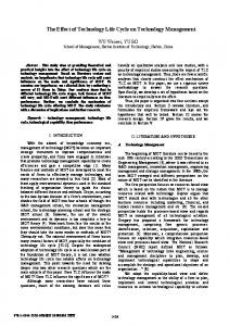
Fig. 1. Micro-CSP joint cross section. TABLE I MINIMUM DIE SIZE FOR EACH MICROCSP ARRAY
Index Terms—Darveaux model, finite element analysis, microCSP, solder joint reliability.
I. INTRODUCTION
M
ICROCSP is an ADI wafer level chip scale package, the only true chip-size package. The die itself is the package. Eutectic solder bumps (63% tin, 37% lead) are connected to the active side of the die (either directly to the bond pads or through a redistribution layer). The MicroCSP part can then be mounted onto the customer’s printed circuit board using standard surface mount assembly techniques. In comparison to other packaging techniques, MicroCSP technology offers a number of significant benefits, such as [1], [2]. 1) Reduction in board space occupied, as die size equals package size. 2) Improved electrical performance, e.g., reduced inductance, due to the elimination of wire bonds and leads as used in standard plastic packaging.
Manuscript received December 17, 2004; revised April 1, 2005. This work wa supported by the Integrated Electronics Engineering Center (IEEC), State University of New York, Binghamton and Analog Devices Inc., Wilmington, MA. This work was recommended for publication by Associate Editor K. Jonnalagadda upon evaluation of the reviewers’ comments. S. C. Chaparala, B. D. Rogeman, J. M. Pitarresi, and B. G. Sammakia are with the Department of Mechanical Engineering, State University of New York at Binghamton, Binghamton, NY 13902-6000 USA (e-mail:
[email protected];
[email protected];
[email protected];
[email protected]). J. Jackson, G. Griffin, and T. McHugh are with Analog Devices, Inc., Norwood, MA 02062 USA. Digital Object Identifier 10.1109/TCAPT.2005.853589
3) Thinner package profile (with considerable weight reduction) due to elimination of lead frame and molding compound. 4) No underfill required and standard SMT assembly equipment and processing can be used. 5) High assembly yields can be realized from the selfaligning characteristic of the low mass die during solder attachment. A schematic of the cross section of a typical MicroCSP joint is shown in Fig. 1 after reflow attachment. All MicroCSP parts from ADI have a standard pitch of 0.5 mm and a standard bump diameter of either 0.320 mm (large bumps) or a 0.180 mm (small bumps). For this reason, each array offered has a minimum die size (and hence package size) to accommodate the standard bumps and pitches. For an array pitch of 0.5 mm and a ball size approximately 320 m wide, the various standard MicroCSP arrays that are offered are listed in Table I. The actual standoff of solder joints after assembly will vary with the amount of solder screened on the substrate, weight of the die, wetted area, and so on. Typical dimensions for solder joint height for a die thinned to 14 mils are 220 m for a larger ball and 115 m for a smaller ball [3]. If the die is too small to accommodate 320- m diameter balls, or a thinner mounted device is required, then the smaller ball size (180 m) can be considered. For example, five ball 2 1
1521-3331/$20.00 © 2005 IEEE
442
IEEE TRANSACTIONS ON COMPONENTS AND PACKAGING TECHNOLOGIES, VOL. 28, NO. 3, SEPTEMBER 2005
III. CONSTITUTIVE RELATION AND MODEL CORRELATION
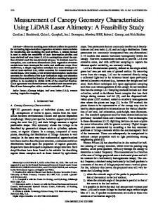
Fig. 2.
Layout of 16 I/O MicroCSP.
(center of die) 2 array of 180- m diameter balls will enable a die size of 1.3 mm 0.9 mm to accommodate the five balls at 0.5-mm minimum spacing. The reliability of MicroCSP is a key issue because the difference in the thermal expansion between the die and the substrate causes viscoplastic deformation and low cycle fatigue of solder joints when the package is subjected to thermal cycling. In order to design a reliable MicroCSP package, it is essential to assess critical geometric factors, which affect the durability of solder joints. It is also beneficial to optimize the effects of thermal cycle parameters on the fatigue life of solder joint. The reliability of wafer level CSP joints has been investigated in recent literature [4]. These studies report finite element analysis to obtain predictions of the durability of solder joints. We have two objectives in this study. One is to examine the effects of geometric parameters such as die and board thicknesses, die size, solder joint height and diameter. The other is to investigate the effect of thermal cycling test parameters such as dwell time, ramp rates, and temperature range. The 16-bump package used as the primary vehicle for modeling in this work is a large bump (325 m bump diameter) device, with a 0.5 mm bump pitch. The bump layout is an area array, covering the full area of the active face of the IC. Fig. 2 shows an illustration of the device.
Accurate constitutive modeling of the solder plays an important part in the solder joint reliability model. Unifying plasticity and creep through a set of flow and evolutionary equations, Lalit Anand developed a constitutive model for hot working of metals [5]. There are two basic features in Anand’s model applicable to an isotropic rate-dependent constitutive model for metals. First, there is no explicit yield surface. Rather, the instantaneous response of the material is dependent on its current state. Secondly, it assumes plasticity from the very beginning of the analysis. The inelastic strain rate in Anand’s model is dependent on temperature and stress. Anand did not consider rate-independent plasticity in his constitutive model. Therefore, Darveaux, et al., [6] were the first to modify the constants in Anand’s constitutive relation to account for both time-dependent and time-independent phenomenon. Parameters for neareutectic 62Sn/36Pb/2Ag solder are given in [6]–[8]. Anand’s constitutive model in ANSYS (Version 6.1) requires the use of an element capable of viscoplastic response. Such element types are available for both two- and three-dimensional (3-D) modeling in ANSYS. In addition, these elements have, as a standard output, viscoplastic work. This parameter was used in the solder fatigue model that is employed in this paper. In addition to solder constitutive modeling, energy based metric for predicting crack initiation and growth in solder joints was also developed by Darveaux, et al. [6]. Over the years, this method has been further refined [7], [8]. The two major (the number constituents of the crack growth rate model are of cycles to crack initiation) (1) and
II. RELIABILITY TEST PROGRAM Assemblies of the 16-bump device were built for solder joint reliability testing All the sample lots consisted of parts mounted on 0.8 mm thick FR-4 boards. The devices were all daisy chain type. Pad to adjacent pad connects within the array were routed in the top layer and microvia connections used to route outside the array. The board pads had 275- m diameter, nonsolder mask pad-defined geometry. A DEK 260 stencil printer was used to print solder onto the board pads using an electroformed stencil that was 125 m thick and had 250- m square apertures. A Zevotech 575 was used for the pick-and-place operation and was followed by reflow in a Vitronics convection reflow furnace. 32 units were assembled per board panel. An aluminum skeleton frame was used to keep the board from warping in temperature cycling but did not constrain the expansion and contraction. The boards were mounted into slots of a stainless steel cage in the thermal chambers. In-situ electrical monitoring of the test units was applied. A failure was defined as 300 in total resistance across the daisy chain. Cumulative as well as time-point specific failures were recorded and were plotted to obtain the necessary experimental Weibull constants. This data is compared in later sections with the results from modeling to check for model accuracy.
(crack growth rate per cycle,
) (2)
where , , , and are the constants that are dependent is the volume averaged viscoplastic on the element size. strain energy density increment per cycle. These two major constituents are combined to predict the characteristic fatigue life ( ) of the solder joint with the pad of diameter ‘ ’ on package side, thus (3) At the corner of the solder joint and pad for typical ball type joints, certain stress and strain components (and, therefore, viscoplastic work) show a high degree of sensitivity to the element size used to model that region. Consequently, convergence studies were performed to provide guidelines for element thicknesses at this critical interface [7], [8]. From these guidelines, a mesh of elements with acceptable aspect ratios is constructed. Darveaux’s technique accounts for the singularity problem at the interface by a two-pronged method. First, the four constants , , , and used in (1) and (2) were identified for a range of element thickness as shown in Table II. Second, the
CHAPARALA et al.: EFFECT OF GEOMETRY AND TEMPERATURE CYCLE
443
TABLE II SUGGESTED CONSTANTS FOR USE IN PREDICTING SOLDER FATIGUE WITH (1)–(3)
TABLE III ROOM TEMPERATURE MATERIAL PROPERTIES USED IN THE FINITE ELEMENT MODEL
TABLE IV CORRELATION BETWEEN EXPERIMENTAL OBSERVATIONS AND FINITE ELEMENT SIMULATIONS [4]
Fig. 3. General view of octant symmetric finite element model of 16-I/O MicroCSP test sample.
stabilized viscoplastic strain energy density per cycle was extracted after the third thermal cycle of the simulation and then volume averaged across the crack interface. The commercial finite element code ANSYS was used to determine the mechanical response of the MicroCSP mounted to a four-layer 0.8 mm thick FR-4 board as it was subjected to the thermal profile of 40 C to 125 C. A generic octant-symmetric finite element model of the MicroCSP package family was built. This model included a number of parameters that allowed changes in the package geometry to be made easily. Three-dimensional elements were used throughout. Fig. 3 shows a general view of a typical MicroCSP octant-symmetric finite element model showing the general region of applied boundary conditions. Since the solder joints were daisy-chained electrically and the fault detection apparatus does not discriminate among the joints that failed, a method for estimating the package reliability was required. The following summarizes the methodology used for for a component establishing the mean cycles to failure based upon the predicted for a group of solder joints. A two-parameter Weibull failure distribution was assumed. The reliability or number of survivors, for a two-parameter Weibull distribution is given as (4) is the reliability, and is the number of cycles to where (the charachieve that reliability. The two parameters are acteristic life), and (the shape parameter or Weibull slope).
For a series of joints connected electrically, the overall reliability of all the joints is given by the product of the reliability of each joint in the series. With the characteristic life of each joint computed from the finite element calculations using the crack growth rate approach [(1)–(4)], the cycles-to-failure versus reliability relationship can then be generated for any assumed shape parameter. In computing the fatigue life of the solder joint, three complete thermal cycles were simulated. This was done to stabilize the response of the model so that a converged value of the viscoplastic work increment was obtained. The cyclic volume averaged viscoplastic work was taken as the difference between the second and third cycles. The failure mechanism observed in the packages was a fatigue crack located on the die side of the package, just below the UBM. This was also the site of highest viscoplastic work in the model. Consequently, the layer of elements directly beneath the UBM was used for this computation ). of the volume averaged viscoplastic work increment ( The measured Weibull slope is 9.7 for thermal cycle 40 to 125 C. While it is observed from experiments, the package reliability is 1010 cycles, the model predicted 1200 cycles, which is within 20% of the measured values. This is well within the range for absolute predictions often reported expected for this approach. [6]–[8]. Also the previous study by same authors on the similar package with different number of I/Os and under different testing conditions indicates the good correlation between the finite element predictions and experimental observation in three cases (see Table III). Table IV [4] provides the details. IV. RESULTS AND DISCUSSION Having obtained good correlation between experimental and predicted values in the four different cases under different test
444
IEEE TRANSACTIONS ON COMPONENTS AND PACKAGING TECHNOLOGIES, VOL. 28, NO. 3, SEPTEMBER 2005
Fig. 4. Close-up view of the finite element model for the 16 I/O MicroCSP.
Fig. 6.
Effect of die thickness on the solder joint reliability.
TABLE V SOLDER JOINT SIZE USED IN THE STUDY
Fig. 5.
Effect of die size on the solder joint reliability.
conditions, several parametric studies have been done to obtain optimum design variables using this finite element modeling method (see Fig. 4). A. Effect of Geometric Parameters Different sizes of die were considered to study the effect of the die size on the solder joint reliability. The size of the die in the primary test vehicle is 2 mm 2 mm. It is a 16 I/O package. Other dies considered are 3 mm 3 mm which is 36 I/O package and 4 mm 4 mm which is 64 I/O package. It is observed that as the die size is increased, the reliability of the package is decreased. Fig. 5 shows the variation of cycles to failure with increasing die size. This is because as the die size is increased, the distance from neutral point increases which leads to more strain in the solder joints. Three different cases were investigated to study the effect of die thickness. These studies have been carried out on two different boards of thicknesses of 0.8 mm and 1.6 mm. It can be observed from Fig. 6 that the solder joint life decreases as the die thickness increases. Also, the package shows better performance on a thinner board, which is because the thinner boards are more compliant, thus reducing the amount of viscoplastic work in the solder joints.
Fig. 7. Effect of solder joint height on the solder joint reliability.
Two different solder sizes are investigated. Table V shows the details of the solder joint sizes used in this study and corresponding reliability in each case. The total number of balls is still 16 in the package. Fig. 7 shows the variation in the cycles to failure as a function of solder joint height. This is because as the size of the ball increases, the crack length increases and the time for crack propagation increases. Also the stand off increases, which makes the solder joint compliant than the smaller balls. These factors increase the solder joint life.
CHAPARALA et al.: EFFECT OF GEOMETRY AND TEMPERATURE CYCLE
Fig. 8. Effect of dwell time on the solder joint reliability.
445
Fig. 9. Effect of ramp rate on the solder joint reliability.
B. Effects of Temperature Cycle Although finite element analysis is extensively used in the durability analysis of the WLCSP assembly, tests of the assembly under thermal cycling loads are necessary to verify the numerical results and identify the failure mechanism. Such reliability tests are very time- and cost- consuming. In order to design the optimum temperature profile for tests, it is useful to study the effects of various thermal cycling parameters on the durability of the WLCSP packages. In this study, a set of temperature profiles is applied on the reference geometry to study the effects of ramp rate, dwell time and temperature range. The constants provided in Table II were used in all the simulations below to calculate the cycles to failure. No experimental test data is available to support the results from the simulations under the test conditions considered in these parametric studies. The effect of varying dwell time on solder joint fatigue life is shown in Fig. 8. These analyses are conducted with a temperature range of 165 C. ( 40 C to 125 C) and a ramp rate is . It is found that visco plastic work increases as dwell 11 C time increases. This reflects the accumulation of creep damage with time. Cycles to failure decreases with increasing dwell time because creep damage dominates in the cases studied here. Time to failure increases with dwell time because the influence of the increase in dwell time exceeds that of the reduction in cycles to failure. This points to the need for reducing the dwell time when designing the temperature cycling tests. Ramp rate is another important parameter in the temperature profile. Its effect on the solder joint fatigue life is shown in Fig. 9. In this analysis, ramp rate changes from 11 C to 88 C while dwell time is fixed at 15 min, temperature range at 165 C. It is found that the visco plastic work increases as ramp rate increases. When the temperature range is fixed, lower ramp rate leads to longer ramp time. Although longer ramp times leads to more inelastic strain, the internal stresses substantially decrease due to stress relaxation. When the contribution of stress relaxation exceeds the influence of the increase in creep strain, the creep strain energy density will actually be reduced. Therefore, the lower the ramp rate, the smaller the creep energy density. It also leads to an increase in cycles to failure. In addition, time to failure decreases very rapidly at first
Fig. 10.
Effect of temperature range on the solder joint reliability.
with increasing ramp rate but becomes nearly constant beyond certain ramp rate. C to 125 C and The temperature range is changed from 55 C to 150 C from 40 C to 125 C to study its effect on visco plastic strain energy density and solder fatigue life. The results are shown in Fig. 10. Ramp rate and dwell time are kept then same. As expected, the viscoplastic work increases as temperature range increases and thus the solder joint reliability decreases. It is obvious that increasing the temperature range under practical test conditions is an effective way to reduce the time and cost of the reliability tests. The melting point of solder and lowest environment temperature are the limits on the temperature range [9]. V. MOIRE MEASUREMENTS Component warpage is one important consideration in determining an acceptable yield for attaching packages to circuit boards. The warpage behavior for a given sample may change throughout the manufacturing cycle, for example, as the assembly travels through reflow processing. At reflow
446
IEEE TRANSACTIONS ON COMPONENTS AND PACKAGING TECHNOLOGIES, VOL. 28, NO. 3, SEPTEMBER 2005
The ADI 4 4 area array, 16 I/O package was prepared according to the standard sample preparation steps in Shadow Moiré Technique and out-of-plane measurements were taken at room temperature, 183 C and 220 C during heating. After reaching the peak temperature, the die de-soldered and became stuck to the part of the testing apparatus, so measurements during cool down were not made. The curvature of the sample was measured across the diagonals, since that is the greatest length, and thus should exhibit the highest deflection. The 3-D plots of the top surface of the die are included below. This gives a more visual understanding of the surface shape. The initial state of the top of the die is not flat (see surface images below). Heating to 183 C does not change this curvature, however, at 220 C, there is noticeable change. At 220 C, the warpage increases by 0.1 mils (2.54 m) near the edges. At 220 C, the initial curvature of the surface at the center has flattened. Moiré interferometry is an optical technique for measuring displacement in a specimen. The results of a moiré analysis are full-field in-plane displacements in the form of a fringe pattern viewed on the surface of the specimen. The equations that govern the relationship between fringe order and in-plane displacement are expressed as
(8)
Fig. 11.
Warpage measurements at different temperatures.
temperatures, component warpage in combination with that of the circuit board, can lead to product failures including open solder joints or bridging of interconnects. The motivation for performing Shadow-Moiré during a simulated reflow cycle is to examine component warpage behavior, as it would occur during the assembly process. This study provides an understanding of the mode of the failure of the solder joints during accelerated thermal cycling.
and are the in-plane displacement fields in the Here, - and -directions, respectively, and and are their respective fringe orders. The quantity is the frequency of the reference grating. For electronic packaging applications the in-plane displacements can be measured with an accuracy of 0.417 m per fringe order. Computer processing of the image data can enhance the resolution of the fringe orders [10]. The 16-bump MicroCSP was cross-sectioned to expose a row of solder joints for moiré displacement analysis. The sample and grating (mounted on a ultra-low expansion glass substrate) were pre-heated in an oven at the 100 C. The sample and substrate were removed from the oven and a thin, even layer of high temperature, low viscosity epoxy was applied to the surface of the sample using an optical grade tissue. The sample was then pressed onto the substrate and placed back into the oven to cure the epoxy [10]. Care was taken to ensure that the sample was not out of the oven for an extended period, as this can lead to errors in the measurement [11]. Once the epoxy was cured, the sample and substrate were taken from the oven and the substrate was removed from the sample, leaving the grating attached to the sample. The sample then cooled to room temperature. An identical micro SMD sample was instrumented with a thermal couple and the cool down curve was recorded and is shown in Fig. 12. Once the part was cooled, it was placed into the interferometer. After setup and calibration, the fringe shifting technique was used to obtain a series of interference pattern images [10]. These were post-processed with the resulting computer enhanced close-up of the fringe patterns shown in Fig. 13 representing contours of horizontal displacement.
CHAPARALA et al.: EFFECT OF GEOMETRY AND TEMPERATURE CYCLE
447
VI. CONCLUSION
Fig. 12.
Measured cooling curve.
In this study, a nonlinear finite element model and Anand’s constitutive relation are used to investigate the effects of geometric parameters and the cyclic temperature profile on the viscoplastic response and the fatigue life of solder joints in WLCSP assembly subjected to thermal cycling. The predicted fatigue life of the package showed very good agreement with measurement. The predicted life from the finite element model was within 20% of the measured life for the thermal profile considered in this paper. It is found that the larger the solder joint, the longer the solder fatigue life. Thinner die on thinner board shows significantly high solder joint reliability. Increase in die size with the increase in number of interconnections reduces the over all package reliability. Dwell time, ramp rate and the temperature range affect the solder joint fatigue life of solder joints in the WLCSP assembly. The longer the dwell time, the longer the time to failure. The larger the ramp rate, the shorter the time to failure. The larger, the temperature range, the shorter the time to failure. Combining small dwell times, suitable ramp rate and large temperature range can optimize the temperature profile for accelerated testing of solder interconnects durability. It was observed that the horizontal displacement in the solder bump was predicted within 10% of the measured displacement from a moiré analysis. REFERENCES
Fig. 13. Close-up of computer enhanced moiré fringe contours of horizontal displacement on outside bump (circled) of 16 I/O MicroCSP. Contour interval is 100.4 nm.
Using the computer model to simulate the cool down from 100 C to room temperature (using the measured cool down curve shown in Fig. 12), the resulting relative horizontal displacement between top and bottom of the end-row solder joints was computed. For these packages, the horizontal displacement (shear displacement) typically dominates the response and is a leading contributor to fatigue damage in the solder joint. This displacement is compared to that measured from the moiré technique. The end joint, shown circled above in Fig. 13, shows approximately five contours from the bottom to the top of the bump. Since each contour is 100.4 nm, the displacement of the end joint in horizontal direction is 502 nm. The quarter-symmetric finite element model was built so that it had the same geometry as the cross-sectioned sample. The model was then loaded using the measured cool down curve of Fig. 11. The relative displacement predicted by the model for the same bump was 552 nm. Comparing to the measured displacement, the model predicts a difference of approximately 10%. This is a satisfactory correlation and adds confidence in the solder constitutive model.
[1] P. Garrou, “Wafer level packaging has arrived,” Semicond. Int., pp. 119–128, Oct. 2000. [2] N. Kelkar, R. Mathew, H. Takiar, and L. Nguyen, “Micro SMD–A wafer level chip scale package,” IEEE Trans. Adv. Packag., vol. 23, no. 2, pp. 227–232, May 2000. [3] J. Jackson, “MicroCSP Wafer Level Chip Scale Package,” Tech. Rep., Application Notes AN-617. [4] J. Pitarresi et al., “A parametric predictive solder joint reliability model for wafer level chip scale package,” in Proc. ECTC’02, San Diego, CA, 2002, pp. 1323–1328. [5] L. Anand, “Constitutive equations for hot-working of metals,” Int. J. Plasticity, vol. 1, pp. 213–231, 1985. [6] R. Darveaux, “Effect of simulation methodology on solder joint crack growth correlation,” in Proc. ECTC’00, Las Vegas, NV, 2000, pp. 1048–1063. [7] R. Darveaux, K. Banerji, A. Mawer, and G. Dody, “Reliability of plastic ball grid array assembly,” in Ball Grid Array Technology, J. Lau, Ed. New York: McGraw-Hill, 1995. [8] R. Darveaux, “Solder joint fatigue life model,” in Proc. TMS Annu. Meeting, Orlando, FL, 1997, pp. 213–218. [9] N. Kelkar et al., “Wafer level chip scale packaging – Solder joint reliability,” in Proc. Int. Symp. Microelectronics (IMAPS’98), San Diego, CA, Nov. 1–4, 1998, pp. 868–875. [10] D. Post, B. Han, and P. Ifju, . New York: Springer-Verlag, 1994. [11] J. Rayner and J. M. Pitarresi, High Sensitivity Moiré. Cincinnati, OH: Soc. Exp. Mech., 1999, pp. 11–14.
Satish C. Chaparala received the B.S. degree in mechanical engineering from the Birla Institute of Technology and Science, Pilani, India, and the M.S. degree in mechanical engineering from the State University of New York at Binghamton, where he is currently pursuing the Ph.D. degree. His research interests include analytical, numerical and experimental investigation of die level stresses in electronic packages, mechanical shock and drop modeling, and solder joint reliability modeling. Mr. Chaparala is a member of ASME.
448
IEEE TRANSACTIONS ON COMPONENTS AND PACKAGING TECHNOLOGIES, VOL. 28, NO. 3, SEPTEMBER 2005
Brian D. Roggeman received the B.S. and M.S. degrees in mechanical engineering from the State University of New York at Binghamton, where he is currently pursuing the Ph.D. degree. His research interests include investigation of in-plane and out-of-plane deformation in electronic packages using Moire Interferometry, mechanical shock and drop testing of electronic equipment, and solder joint reliability testing.
James M. Pitarresi received the B.S., M.S., and Ph.D. degrees from the Civil Engineering Department, the State University of New York at Buffalo, in 1981, 1983, and 1986, respectively. From 1986 through 1987, he served as a post-doc at the National Center for Earthquake Engineering, where he worked on problems of large-scale structural vibration and control. In 1988, he joined the faculty of the Department of Mechanical Engineering, State University of New York at Binghamton (SUNY Binghamton). He has published numerous papers in the field of electronic packaging. In addition, he has co-authored one textbook in the field of solid mechanics. He is currently the Chair of the Department of Mechanical Engineering, SUNY Binghamton. His current research areas include computational mechanics, shock and vibration testing and simulation, and electronics reliability.
Bahgat G. Sammakia received the B.S. degree in mechanical engineering from the University of Alexandria, Alexandria, Egypt, in 1977 and the M.S. and Ph.D. degrees in mechanical engineering from the State University of New York at Buffalo in 1980 and 1982, respectively. He is Director of the Integrated Electronics Engineering Center and is the Executive Director for Economic Development, State University of New York at Binghamton (SUNY Binghamton). His research work was in the areas of natural convection heat transfer. After graduating from SUNY Buffalo, he worked at the University of Pennsylvania, Philadelphia, as a Postdoctoral Fellow. He joined IBM in 1984, where he continued to work until 1998. He is the Editor of the ASME Journal of Electronic Packaging. Dr. Sammakia is a Fellow of the ASME.
John Jackson, photograph and biography not available at the time of publication.
Garry Griffin, photograph and biography not available at the time of publication.
Tom McHugh, photograph and biography not available at the time of publication.