realize 3-D microstructures and MEMS devices, we have proposed the analytical ... typically fabricated using LIGA (German acronym for LIthographie, ...
Effective 3-D Process Modeling and Parameters Determination on Double Exposure in Deep X-ray Lithography
Yoshikazu Hirai, Naoki Matsuzuka and Osamu Tabata
Abstract This paper describes a new analytical method to determine process parameters on Double Exposure in Deep X-Ray Lithography (D2 XRL).
D 2 XRL is a unique and
promising technique for 3-dimentional (3-D) microfabrication among 3-D X-ray lithography techniques.
By way of example, it was demonstrated that a
micro-projection array with a very sharp tip is easily and successfully fabricated without any special apparatus.
In order to advance the capabilities of D2 XRL to
realize 3-D microstructures and MEMS devices, we have proposed the analytical method that is possible to calculate resist profiles of a 3-D microstructure fabricated by D 2 XRL.
The advantage of the newly proposed analytical method is that an effective
relationship between resist profiles and process parameters on D 2 XRL is derived directly from relational expressions.
By the comparisons between resist profiles
calculated by the analytical method and experimental results, it was successfully confirmed that this approach provides an easy way to realize the target micro-projection structures with an acceptable accuracy.
Department of Micro Engineering, Graduate School of Engineering, Kyoto University, Yoshida-Honmachi, Sakyo-ku, Kyoto 606-8501, Japan
1. I NTRODUCTION Standard high-aspect-ratio Micro Electro Mechanical Systems (MEMS) are typically fabricated using LIGA (German acronym for LIthographie, Galvanoformung, Abformung) or other processes, e.g. Deep Reactive Ion Etching (DRIE), micro Electro-Discharge Machining (EDM), and UV lithography using SU-8 ® .
The LIGA
process is one of the most promising MEMS fabrication techniques, and this employs Deep X-Ray Lithography (DXRL) to produce plastic microstructures with feature sizes down to 0.1 µm.
Conventional DXRL is good at fabricating high-aspect-ratio
microstructures with vertical sidewalls.
However, this technique has very limited
controllability of the cross-sectional shape of 3-dimentional (3-D) microstructures. In order to apply DXRL to various fields such as MEMS devices and medical devices, several 3-D X-ray lithography techniques and its extension have been proposed by various research groups [1-3].
Compared with the previously reported 3-D X-ray
lithography techniques, Double exposure in Deep X-Ray Lithography (D2 XRL) shown in Fig. 1 is a unique and promising technique for 3-D microfabrication.
By way of an
example, it was demonstrated that a micro-projection with the very sharp tip is easily and successfully fabricated without any special apparatus [4]. In order to advance the capabilities of D2 XRL to fabricate 3-D microstructures for MEMS devices, this study is aiming at an establishment of an effective analytical method of D 2 XRL process which facilitates the realization of target 3-D microstructures precisely.
The advantage of the newly proposed analytical method is,
once “dissolution rate as a function of depth z” is determined, effective relationship X-ray exposure X-ray Mask
PMMA (a)
(b)
Development process
(d)
(c)
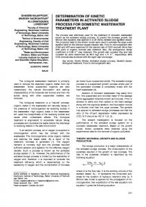
Fig. 1. Schematic illustration of the process steps in D 2 XRL (Step; (a) Æ (b) Æ (c)): (a) the normal exposure step; (b) the mask-less exposure step; (c) the image of fabricated structure by normal and mask-less exposures (i.e. D 2 XRL); (d) the image of fabricated structure by normal exposure (i.e. DXRL).
between resist profiles and process parameters on D2 XRL is derived directly from relational expressions.
In this paper, a micro-projection was utilized as an example to
demonstrate a validity of the analytical method and a verification of prediction accuracy through experiments is described.
2. D ESCRIPTION OF 3-D P ROCESS M ODELING 2.1 P ROCESS S TEPS AND M ECHANISM OF D 2 XRL [4, 5] Figure 1 shows the process steps of the micro-projection structure by D2 XRL using an X-ray mask with a circular absorber.
If a poly-methylmethacrylate (PMMA),
the most commonly used positive-tone thick photoresist in X-ray lithography, is developed after the exposure process (step: (a) Æ (d)), a cylindrical microstructure with the vertical sidewall is fabricated.
In D2 XRL, a mask-less exposure as shown in
Fig. 1 (b) is combined with a normal exposure before the development process.
On
2
D XRL technique, the major process parameters are a combination of deposited dose on 1st and 2nd exposure steps and a development time as shown in Fig. 2.
The tip
angle tends to be sharpened when the ratio of the deposited dose on exposure (a) to the deposited dose on exposure (b) is higher.
Figure 3 shows schematic of dose
distribution in a PMMA depth direction given by D 2 XRL and a simplified development behavior.
The development behavior to realize the micro-projection can be
understood as follows.
In the development process, the area A dissolves faster than
area B because the dissolution rate increases exponentially to dose. formed at the boundary between area A and B regions.
Then, a step is
Since development is
isotropic, the sidewalls of the steps are exposed to the developer and developed. leads to rounding of corners and sidewall inclination.
This
The theory for understanding
these phenomena has been already confirmed in our previous experiments and simulation results [6, 7]. 2.2 3-D P ROCESS M ODELING AND L ITHOGRAPHY S IMULATION S YSTEM (X3D) Development of a resist profile simulation tool and an analytical method to determine process parameter is a major interest among 3-D X-ray lithography research groups.
One explanation for this interest is that there are a lot of complicated process
parameters and difficulty in determining these parameters.
In addition, the most
important point of modeling 3-D X-ray lithography process accurately is that resist profile simulation tool should take into account a dissolution vector as well as the resultant dose distribution.
In that case, the problem is how to model the propagation
Ratio of deposited dose “exposure (a) : exposure (b)” 1.0 : 2.2 2.1 : 1.6
Development time [min]
5 µm
10 µm
5 µm
10 µm
30
120
Fig. 2. SEM images of micro-projection structures with different development time and deposited dose pattern. These structures were fabricated by the X-ray mask with an absorbers pattern of 15 µm in diameter. Deposited dose of “exposure (a)” and “exposure (b)” are corresponding to the exposure step in Fig. 1.
Dissolution vector Color gradient in PMMA A
B
Absorbed dose
A
(a) At the beginning
high
low x
o z A
B
A
A
B
A
(b) Propagation to vertical (c) Propagation to lateral
Fig. 3.
Illustration of the development behaviors in D 2 XRL.
of the dissolution front and calculate its profile at any development time.
So far, the
3-D X-ray lithography simulation system (X3D) [7, 8], which adopted the Fast Marching Method [9] in development process simulation, has been the only approach to be able to handle this problem.
Figure 4 (a) shows the simulated cross sectional
2
view of a resist profiles for D XRL using the Fast Marching Method. shows more detail simulated results in three dimension by X3D. error is required to determine optimal process parameters.
Figure 4 (b)
However trial and
Therefore, a simple
analytical method to determine the process parameters is required to advance the capabilities of D2 XRL to fabricate MEMS devices.
(a)
(b)
Development time = T 0
Development time = T 1
Development time = T 2
Fig. 4. Examples of resist profiles simulation tool for D 2 XRL: (b) X3D.
(a) Fast Marching Method;
3. ANALYTICAL M ETHOD 3.1 C ALCULATION OF R ESIST P ROFILES A concept of the analytical method for the resist profile calculation is shown in Fig. 3.
In this method, the resist profile is calculated by combining individually
calculated vertical and lateral propagations of dissolution front [10].
A schematic of
computational procedure is the follows. 1) Vertical Propagation of Interface:
The relationship between the development
time T and resist depth z is given by Eq. (1) z
T = V ' ( z ) = ∫ R ( z ) −1 dz
(1)
0
where R(z) is the dissolution rate as function of depth z.
Thus, the depth z is given by
−1
z = V ' (T ) .
(2)
Therefore, a resist profile that only takes into account the vertical propagation is calculated by substituting the dissolution rate R A (z) and R B (z), which indicate the dissolution rates for area A and B, respectively.
Next, Eq. (2) is transformed to Eq.
(3) by utilizing the position x and depth z as shown in Fig. 3 (c), z = V −1 ( x , T )
(3)
where
T = V ( x, z) z
= V A ( z ) = ∫ R A ( z ) −1 dz 0
z
= VB ( z ) = ∫ RB ( z ) −1 dz 0
for x at area A for x at area B.
2) Lateral Propagation of Interface:
The propagating length x p from the
boundary between area A and B toward area B is given by z
x p = L( z , T ) = RB ( z )t ( z ) = RB ( z ){T − ∫ R A ( z ) −1 dz}
(4)
0
where t(z) is the lateral propagating time t which is given as a function of depth z. Since x p corresponds to a position along the x-axis, depth z at position x is given as z = L−1 ( x, T ) .
(5)
3) Combined Propagations of the Procedure 1) and 2): (3) and (5), the resist profiles are plotted.
Based on results of Eqs.
Please note that prior knowledge of the
dissolution rate R A (z) and R B (z) is necessary to calculate resist profiles.
This
dissolution rate as a function of depth z is determined by a dedicated experimental method [4]. 3.2 EXPERIMENTS AND VALIDATION OF A NALYTICAL M ODEL
Experiments were carried out at BL-15 of “AURORA” at Ritsumeikan University. In the 1st exposure step (Fig. 1 (a)), PMMA (CLAREX commercialized by Nitto Jushi Kogyo Co., Ltd.) is exposed using the X-ray mask (fabricated by Optnics Precision Co., Ltd.) with an absorbers pattern of 10 µm in diameter.
In the development process, the
GG developer (60 vol% 2-(2-n-butoxyethoxy) ethanol, 20 vol% tetrahydro-1-4-oxazine, 15 vol% de-ionized water, and 5 vol% 2-aminoethanol) was used at a development temperature of 39.0 °C.
The experimental conditions for the fabrication and a resist
profiles simulation were summarized in Table 1. Figure 5 shows the resist profiles of samples number 1 to 2 and 3 to 4. zero corresponds to the original resist surface.
The depth
The comparison between
measurements, simulation results, and error is summarized in Table 2.
From this
result, it is confirmed that the structural shapes are calculated with acceptable accuracy. It is thought that the difference between the measurements and calculated resist profiles was caused by the measurement accuracy of the dissolution rate, and the experimental repeatability.
The improvement of the experimental accuracy will
enable us to calculate the resist profiles more accurately.
Table 1. Experimental conditions for the fabrication and the resist profile simulation of micro-projection: (a) setup parameters for exposure process at BL-15; (b) experimental parameters on sample number of micro-projection. (a) SR (AURORA) Exposure parameter X-ray mask
Operating electron energy Critical wave length Typical source size (vertical) Distance between source to mask Filter (Be) Scan length Absorber (Au) Membrane (Polyimide)
ε λc σy D
0.575 GeV 1.5 nm 0.14 mm 3.88 m 200 µm × 2 20 mm 2.0 µm 50 µm
(b) Deposited dose Development time [min] Mask [A·min] Mask-less [A·min] 3.0 2.0 30 3.0 2.0 60 3.0 3.0 30 3.0 3.0 60
Sample No. 1 2 3 4
(a)
(b) 0
20 3-2-30min 3-2-60min Measured Measured
30
Depth [µm]
Depth [µm]
10
3-3-30min 3-3-60min Measured Measured
20 30 40
40 50 60
50 -15
-10
-5
0
5
10
15
Position from the center [µm]
70 -15
-10
-5
0
5
10
Fig. 5. Comparison between measurements and simulation results of resist profiles; sample No. 1 to 2: (b) sample No. 3 to 4.
Table 2. Sample No. 1 2 3 4
Comparison between measurements, simulation results, and error.
(a) Measurement Height Angle [µm] [deg] 22.1 30.8 24.7 33.7 15.9 45.1 17.9 46.2
(b) Simulation Height Angle [µm] [deg] 22.2 32.7 21.7 35.6 14.9 46.3 14.9 47.1
15
Position from the center [µm]
(c) Difference Height Angle [µm] [deg] 0.1 1.9 -3.0 1.9 -1.0 1.2 -3.0 0.9
(d) Error Height Angle [%] [%] 0.45 6.17 -12.2 5.64 -6.29 2.66 -16.8 1.95
(a)
3.3 D ETERMINATION OF P ROCESS PARAMETERS
The analytical method is useful to determine the process parameters for the target micro-projection.
The advantage of this approach is that the relationship of the
height and tip angle of micro-projection on development time can be derived directly from related equations.
When the absorber pattern is a circle, the height and tip angle
are given by Eqs. (6) and (7) respectively, −1
H = V A−1 (T ) − L−1 ( r , T )
for L−1 (r , T ) − VB (T ) > 0
= V A−1 (T ) − VB−1 (T )
for L−1 ( r , T ) − VB (T ) ≤ 0
−1
(6)
where r is the radius of the X-ray mask absorber pattern,
⎡∂ ⎤ L( z, T )⎥ ⎣ ∂z ⎦ z =h
−1
θ = −2 arctan ⎢ = 180 where r = L(h, T).
for L−1 (r , T ) − VB (T ) > 0 −1
for L−1 (r , T ) − VB (T ) ≤ 0
[deg]
(7)
Figure 6 shows the dependences of the height and tip angle of the
micro-projection on development time. small range from 30.8° to 46.2°.
The measurements of the tip angle show the
The tip angle tends to be sharpened by increasing
the ratio of the deposited dose with the X-ray mask to the deposited dose without the X-ray mask. Fig. 2.
The same tendency was observed in the experimental results shown in
The minimum tip angle (i.e. the sharpest tip angle) confirmed by this method
is 16.6° on the condition that the deposited dose with and without the X-ray mask are 6.0 A·min and 1.0 A·min, respectively, at the development time of 168 min.
The
maximum one is 84.54° on the condition that the deposited dose with and without the
(a) 30
(b) 200 E :E =3:2Amin
Height [µm]
1
2 2
E :E =3:2Amin
Sample No. 2
20
1
Sample No. 4 Sample No. 3
15 10
2
E :E =3:3Amin 1
Sample No. 1
Tip angle [deg]
1
E :E =3:3Amin
25
2
150
100 Sample No. 4 Sample No. 3
50
5 Sample No. 2
Sample No. 1
0
0
10
20
30
40
50
Development time [min]
60
0
0
10
20
30
40
50
Development time [min]
60
Fig. 6. The dependence of the height and tip angle of micro-projection on development time; (a) relationship between the development time and the height: (b) relationship between the development time and the tip angle.
X-ray mask are 0.5 A·min and 4.0 A·min, respectively, at the development time of 144 min.
From these results, the validity and efficiency of the analytical method to
determine process parameters were confirmed.
4. CONCLUSION The analytical method to determine the process parameters for D2 XRL was successfully demonstrated with acceptable accuracy through the fabrication of micro-projection.
By
applying
the
analytical
method,
the
parameters
of
micro-projection such as the height and tip angle were calculated easily and quickly. Consequently, the validity of the proposed approach was confirmed for determining the process parameters to realize the target 3-D microstructures.
In future, good control
of process parameters based on the proposed approach may lead to fabrication of MEMS devices.
ACKNOWLEDGEMENT The authors wish to thank SR center staffs for assistance in “AURORA” operation and Mr. Sadamu Kinoshita at Kyoto University for the SEM images.
This paper is
supported in part by Nanotechnology Researchers Network Project, and Center of Excellence for Research and Education on Complex Functional Mechanical Systems (COE program of the Ministry of Education, Culture, Sports, Science and Technology, Japan).
REFERENCES [1]
O. Tabata, K. Terasoma, N. Agawa and K. Yamamoto, “Moving mask LIGA (M 2 LIGA) process for control of side wall inclination”, in Proc. 12th Int. Conf. on Micro Electro Mechanical Systems, FL, January(1999) 252-256.
[2]
S. Sugiyama, S. Khumpuang and G. Kawaguchi, “Plain-pattern to cross-section transfer (PCT) technique for deep X-ray lithography and applications”, J. Micromech. Microeng., 14 (2004) 1399-1404.
[3]
D. Y. Oh, K. Gil, S. S. Chang, D. K. Jung, N. Y. Park and S. S. Lee, “A tetrahedral three-facet micro mirror with the inclined deep X-ray process”, Sens. Actuators A, Phys., A 93 (2001) 157-161.
[4]
N. Matsuzuka, Y. Hirai and O. Tabata, “A novel fabrication process of 3-D microstructures by double exposure in standard deep X-ray lithography”, in Proc. 17th Int. Conf. on Micro Electro Mechanical Systems, Maastricht, The Netherlands, January(2004) 681-684.
[5]
N. Matsuzuka, Y. Hirai and O. Tabata, “A novel fabrication process of 3-D microstructures by double exposure in deep X-ray lithography (D2 XRL)”, J. Micromech. Microeng., 15 (2005) 2056-2062.
[6]
N. Matsuzuka, Y. Hirai, S. Hafizovic, J. G. Korvink and O. Tabata, “Effect of development process in moving mask deep X-ray lithography for 3-D microfabrication”, in Proc. 5th Int. Workshop on High Aspect Ratio Micro-Structure Technology, Monterey, CA, June(2003) 59-60.
[7]
Y. Hirai, S. Hafizovic, N. Matsuzuka, J. G. Korvink and O. Tabata, “Validation of X-ray lithography and development simulation system for moving mask deep X-ray lithography”, J. Microelectromech. Syst., 15(2006) 159-168.
[8]
S. Hafizovic, Y. Hirai, O. Tabata and J. G. Korvink, “X3D: 3-D X-ray lithography and development simulation for MEMS”, in Proc. 12th Int. Conf. on Solid-State Sensors Actuators and Microsystems, Boston, MA, June(2003) 1570-1573.
[9]
J. A. Sethian, Level Set Methods and Fast Marching Methods, 2nd ed. Cambridge, U.K.: Cambridge University Press, 1999.
[10]
Z. Liu, F. Bouamrane, M. Roulliay, R. K. Kupka, A. Labèque and S. Megterty, “Resist dissolution rate and inclined-wall structures in deep X-ray lithography”, J. Micromech. Microeng., 8(1998) 293-300.