Efficient Hardware for Tile-Based Rasterization Dan Crisu, Sorin Cotofana, Stamatis Vassiliadis Petri Liuha Computer Engineering Laboratory, EEMCS NOKIA Research Center Delft University of Technology Visiokatu-1 SF-33720 Mekelweg 4, 2600 GA Delft, The Netherlands Tampere, Finland Phone: +31 15 2783644 Fax: +31 15 2784898 E-mail:
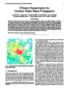
[email protected] E-mail: {dan|sorin|stamatis}@ce.et.tudelft.nl Abstract— An efficient logic-enhanced memory architecture is presented that solves existing problems associated with 3D graphics tile-based hardware rasterization algorithms. The memory contains the same number of bits as the number of pixels in the tile, and during rasterization time it is filled up in several clock cycles by a systolic primitive scanconversion subsystem with the stencil of the primitive: ones are written for memory locations that represent tile pixels covered by the primitive, otherwise zeros are stored. Once the shape of the primitive has been coded inside the memory, the memory internal logic is capable of delivering, on request, up to four hit positions (tile positions inside the primitive) per clock cycle to the pixel processing pipelines, signaling when all the hit positions were consumed. Employing our proposed memory architecture no searching overhead is needed to find the first hit position inside the primitives. Furthermore “ghost” primitives are handled efficiently with a small constant delay irrespective of the primitive size. Finally, hit positions (communicated in a spatial pattern to increase texture cache hit ratios) can always be mapped to different memory banks in the Z-buffer or colorbuffer breaking the “read-modify-write” dependency associated with depth test and color blending. Hardware implementation in a commercial 0.18µm process technology for a QVGA 3D graphics hardware accelerator with a tile size of 32 × 16 pixels has indicated that the memory can be clocked at 200MHz and consumes an area of 120000µm2 . Keywords— 3D graphics architectures; tile-based rasterization; embedded systems; memory architectures.
I. I NTRODUCTION The challenge posed by the formidable cost constraints on products for the mobile consumer market requires a new breed of graphics rendering hardware with very low power consumption and implementation costs which precludes the utilization of the advanced features and the high throughput achieved in high-end systems. To fulfil these design constraints, tiling or chunking architectures [1] were proposed as a way to save memory bandwidth on framebuffer accesses, since an external memory access typically is one of the most energy-consuming operations, and to counteract the huge increase in storage re-
y
Bounding Box of T Bounding Box & Triangle Overlap
C 2
Only Bounding Box Overlap
No overlap 1
T(A,B,C)
B
1
2
A 0
0
3
x
Fig. 1. “Ghost” triangle for tiles (0, 2), (1, 0), (2, 0), and (2, 2).
quired by full-scene antialiasing. In a tiling architecture, the screen is divided in a number of non-overlapping regions, or tiles, which are processed serially. Every frame, primitive geometry is sorted first by screen location and dumped into one or more bins, one bin per tile. Geometry that overlaps a tile boundary is referenced in each tile it is visible in. When all the primitive geometry has been specified, it is rendered from bin N to the tile N before moving to the tile N + 1. The advantage of the tile-based architectures is that all the data (colors, depth) can be maintained in on-chip tile-sized buffers and accesses to external memories are required only to dump the tile color buffer content to the global off-chip frame buffer when all the primitive geometry for the current processed tile at the current frame was rasterized. In traditional full-screen architectures efficient rasterization algorithms [2][3] are based on edge functions [4] and rely on the following paradigm: while not all the positions inside the primitive are exhausted do 1) save the rasterization context, 2) move to a new rasterization position, 3) test the edge functions value for that position to see if the position is a hit, 4) if it is inside communicate this hit position to the pixel processing pipelines and update the rasterization context else restore the rasterization context, 5) based on the edge functions computed earlier try to predict a new hit position. The main difficulty in tile-based rasterization with this algorithm is to find the first hit position in the to be rasterized primitive, from our experiments the overhead can be
352
50%-300% (including testing if any of the primitive vertices or the primitive center of gravity are in the current rasterized tile to be considered the starting rasterization position or the hit point). In addition there is always overhead associated with ”ghost” primitives (depicted in Figure 1), primitives that are assigned to the current tile when they have nothing in common with it (this is due to the simple software driver algorithm that assigns primitives to tiles based on a primitive bounding box test; other more complex tests in the software driver were envisaged eliminating the ”ghost” primitive problem completely but moving the costs to software). In full-screen rasterization this overhead is inexistent due to the fact that a starting point inside the primitive can always be found, e.g., the center of gravity. In addition, several studies [5], [6], [7] have revealed that the primitive pixel rasterization order is crucial for low-cost tile-based architectures that don’t have dedicated texture memories (pull texture architectures) and are relying on a robust texture cache hit ratio to reduce the latency and energy consumption of texel fetches from the external system memory. To overcome the previously mentioned problems we propose an efficient logic-enhanced memory architecture to accelerate primitive traversal in 3D graphics tile-based rasterizers. The memory contains the same number of bits as the number of pixels in the tile, and during rasterization time it is filled up in several clock cycles by a systolic primitive scan-conversion subsystem with the stencil of the primitive: ones are written for memory locations that represent tile pixels covered by primitive and zeros for the rest. Once the shape of the primitive has been coded inside the memory, the memory internal logic is capable to deliver, on request, to the pixel processing pipelines at least one and up to four hit positions per clock cycle while signaling when all the hit positions were consumed or if none existed. The logic-enhanced memory architecture presents the following benefits: it handles “ghost” primitives efficiently, hit positions are communicated in a spatial pattern that increases the hit ratio of texture caches in pull texture architectures, and hit positions can always be mapped to different memory banks in the Z-buffer or color-buffer breaking the “read-modify-write” dependency associated with depth test and color blending thus allowing efficient pipelining. Hardware implementation in a typical 0.18µm process technology for a QVGA 3D graphics hardware accelerator with a tile size of 32 × 16 pixels has indicated that the memory can be clocked at 200MHz and consumes an area of 120000µm2 . The rest of the paper is organized as follows. The logicenhanced memory architecture is described in Section II.
Quad 11 (Group 10, Block 00)
8 Pixel
7 6 5 4 3 2 y
1 0
C
D C
D C
D C
D
A
B A
B A
B A
B
C
D C
D C
D C
D
A
B A
B A
B A
B
C
D C
D C
D C
D
A
B A
B A
B A
B
C
D C
D C
D C
D
0
1 x
2
3
B
B A
B A
B A
A
4
5
Block 00
6
7
8
Group 01 (Block 00)
Fig. 2. Proposed pixel rasterization order in tile.
In Section III, hardware implementation results are presented. Finally, in Section IV, the conclusions are drawn. II. L OGIC -E NHANCED M EMORY A RCHITECTURE The quest to an efficient hardware algorithm for rasterization has to start from finding a suitable pixel rasterization order. In Figure 2 the pixel grid of the tile around the origin of the tile coordinate system is depicted and a space-filling path indicated with arrows starting from the origin is presented. Space-filling paths are known to improve the texel coherency generating high hit-ratio in texture caches [1]. In addition, if 2 × 2 regions of fragments can be generated during rasterization they can be mapped on different memory banks A, B, C, D. Supposing that the shape or stencil of a triangle has been already coded in a memory representing the bi-dimensional tile, now hit locations have to be forwarded to the pixel processing pipeline. The most appropriate way to select between many hit locations according to the space-filling path traversal order is via priority encoding. After the hit location was communicated, the bit for that location has to be reset in order for a priority encoding scheme to work further. Referring to Figure 2, an (x, y) offset position can be encoded in terms of block positions (8 × 8 fragment regions), group positions (4 × 4 fragment regions), quad positions (2 × 2 fragment regions), and positions in quad. Assuming a 32 × 16 pixel tile, the location (x, y) = (x4 x3 x2 x1 x0 , y3 y2 y1 y0 ) can be encoded as (Block, Group, Quad, P os) = (y3 x4 x3 , y2 x2 , y1 x1 , y0 x0 ). With this encoding, priority can be restated hierarchically: hit locations in a block (respectively group, quad) encountered earlier on the spacefilling path have a higher priority than any hit locations in a block (respectively group, quad) encountered later on the path (see Figure 3). In the following a logic-enhanced memory architecture
353
Pre
Pre
M2
M1
M9 M4 M3
GrpWrEn
GrpWrEn QuadNZ M8_00
M8_01
M8_10
M8_11
M10 M5
M7
M6
QuadRdClr
InTriWL11
InTriWH11
InTriR11
InTriWL10
InTriWH10
InTriR10
InTriWL01
InTriWH01
InTriR01
InTriWL00
InTriWH00
InTriR00
DLY_BUFF
Fig. 4. Quad Cell.
Pixel Pixel Pixel Pixel 00 01 10 11
Quad
Quad Quad Quad Quad 00 01 10 11
Group
Priority decreasing
Fig. 3. Pixel and Quad coding.
based on a hierarchical priority encoding scheme supporting a tile size of 32 × 16 pixels is presented. The memory is used in conjunction with a systolic primitive scanconversion subsystem, using edge functions, that works on a sliding window of 8 × 8 locations (a block) and outputs every clock cycle the primitive shape (encoded with one bit per location) for a different 4 × 4 pixel region (a group) inside the currently processed block. The sliding window is moved according to the space-filling path traversal order until all the tile locations are exhausted, also the groups generated by the systolic subsystem on the blocksized window are output according to the space-filling path traversal order. The logic-enhanced memory has a word line width equal to the size of a group (16 bits) and is capable of working back-to-back with the systolic subsystem meaning that every clock cycle the primitive shape for a group of locations is transfered inside the memory. The memory contains 32 wordlines (1tile=8blocks×4groups) and can be filled up by the systolic subsystem with the primitive shape in 32 clock cycles. The systolic subsys-
tem sliding window size was designed to lead to hardware costs that match the hardware size of a full-screen rasterizer, therefore larger sizes, although benefic from a performance viewpoint, were considered too costly. The systolic subsystem is described in detail in [8]. Once the shape of the primitive has been completely transferred to the logic-enhanced memory, quads which contain at least a hit location (less than four hit locations if the quad is situated on the primitive edges) will be output at a rate of one per cycle to the pixel procesing pipeline in the proper space-filling rasterization order until all the hit locations are exhausted. The memory output interface includes the individual bits of the quad, the encoding of the quad in the (Block, Group, Quad) format, and a signal that indicates if all the hit locations were transferred out. The (Block, Group, Quad) format is suitable for computations in the subsequent pixel processing stages resulting only in multi-operand additions that can be implemented efficiently as described in [8]. The logic-enhanced memory architecture is presented in Figures 4, 5, and 6. The memory contains 32 wordlines, each wordline contains a group, each group contains four quads, and each quad contains four locations bits. An entire group can be written per clock cycle but only one quad can be read out per clock cycle. For write operations the memory behavior is identical to any CMOS SRAM read/write memory thus it will not be described in detail; further the differential bit lines used for writing are omitted from the drawings. When a quad containing hit locations is requested, the priority tokens of all quad words are trans-
354
Pre Group Priority Encoder QuadCell_00
QuadCell_01
QuadCell_10
GrpNZ
QuadCell_11 LA QuadNZ_00 D0
EP0
D1
EP1
D2
EP2
D3
EP3
QuadNZ_01 QuadNZ_10 QuadNZ_11
QuadRdClr_11
QuadRdClr_10
QuadRdClr_01
GrpPri
QuadRdClr_00
to all GroupCells
Quad Code
Fig. 5. Group Cell.
mitted to the group priority encoder, and all group priority tokens are transmitted to the global priority encoder. After a decision is taken by the global priority encoder on the highest priority quad containing hit locations, information is bounced back only to the group word line containing the quad, the quad being read out and its non-zero bits reset to prepare the memory for the next read. The location information is stored using static RAM bit cells but the logic circuitry is implemented in domino dynamic logic clocked by the precharge signal Pre. The priority encoders are similar to the high-speed low-power n-type domino logic design described in [9]: the 4-bit group priority encoder has one-level lookahead and the 32-bit global priority encoder is constructed from 8-bit priority encoders connected through the third-level lookahead signals. In Figure 4 the Quad Cell circuit diagram is presented where four locations bit cells are depicted. Each bit cell consists of a storage cell (transistors M1, M2, M3, M4 and the two cross-coupled inverters), one of the four parallel transistors (M8) of a distributed domino four-input OR gate (that includes additionally transistors M9 and M10), the conditional read circuitry (transistors M5, M6) and the reset transistor M7. For write operation, when the sig-
nal GrpWrEn is asserted, one of the two storage nodes is pulled down, and the other is pulled up. This requires the pullup in both inverters to be weaker than the series pulldown transistors. The storage cell is write-only because the conditional read signal is formed internally based on the content of the storage cell and the signal QuadRdClr formed outside the Quad Cell (see Figure 5). The role of the OR gate is to detect if hit locations are stored in the quad cell, then the signal QuadNZ will participate in priority encoding in the Group Cell. If based on the priority encoding scheme the quad contains the hit locations with the highest priority in the memory, the signal QuadRdClr will be asserted for the read and clear operation on the quad bits. The static delay buffer DLY BUFF insures that is enough separation in time between reading the quad bits (the precharged read bit line InTriR can be discharged enough to be detected as logic 0 by the chargeredistribution amplifiers) and clearing the quad bits. The size required for DLY BUFF is small because the memory has only 32 word lines. The role of the Group Cell additional logic circuitry presented in Figure 5 is to pass forward the QuadNZ signals from the four Quad Cells to the group priority encoder.
355
Pre
GroupCell_0 Grp_0
QuadCell_00
QuadCell_11
GrpNZ_0
Group Priority Encoder & Logic
D0 EP0
GrpSel 5
Group Decoder (for write operation)
GrpPri_0
Priority Encoder
& Logic
LA
GrpNZ_31 Grp_31
QuadCell_00
QuadCell_11
Group Priority Encoder & Logic
NZ
D31 EP31
InTriR11
InTriR10
InTriR01
InTriR00
GrpPri_31
GrpWriteEn Control
Quad_00 Bit Amplifiers
Quad_11 Bit Amplifiers
Group Drivers
Quad Code Amplifiers
Group & Block Code Amplifiers
4:1
16
4
Quad
Group
QuadCode
GrpCode
BlockCode
MoreNZQuadsLeft
GetNZQuad
Fig. 6. Logic-enhanced memory architecture.
GrpNZ is connected to the lookahead ouput port (LA) of the group priority encoder and signals that at least one of the Quad cells contains hit locations and this is input in the global priority encoder. If the global priority encoder decides that the Group Cell has the highest priority among the other Group Cells the signal GrpPri is asserted. GrpPri together with the priority encoded lines EP from the group priority encoder is anded using four two-input domino AND gates forming QuadRdClr signals for the Quad Cells. In addition two domino OAI gates are used to form the quad code — if a quad having the highest priority exists in the Group Cell then two precharged bit lines are discharged broadcasting the quad code to the memory output. Finally, in Figure 6 the block diagram of the logicenhanced memory is presented. The signals from the Group Cells are input in the global priority encoder that decides which one of the Group Cells has the highest priority. MoreNZQuadsLeft is connected to the lookahead ouput port (LA) of the global priority encoder and signals that at least one of the Quad cells contains hit locations, therefore indicating outside the memory if there are any hit locations left. The quad code returned is used for multiplexing the highest priority quad bits from the highest priority Group Cell, and logic similar to that presented in Figure 5 is used
to generate the block code and group code outputs. The memory input interface contains the GetNZQuad signal that has to be asserted in order for a quad with hit locations to be read out. The rest of the circuitry is identical to any CMOS SRAM read/write memory and thus it is not described in further details. III. H ARDWARE I MPLEMENTATION R ESULTS The logic-enhanced memory was designed at the physical level in a commercial 0.18µm IC manufacturing technology. After the parasitics were extracted from layout the annotated circuits composing the critical path (starting in Quad Cell 11 of the Group Cell 31, going through the global priority encoder than back in the originating cell, than to the Quad 11 Bit Amplifiers, and finally reaching the Quad output port) were simulated using the HSPICE circuit simulator. The results are reported in Table I. The critical path latency translates in a maximum clock frequency of 200 MHz assuming that the precharge and the evaluation phase take half the clock cycle. IV. C ONCLUSIONS An efficient logic-enhanced memory architecture was presented that solves existing problems associated with 3D graphics tile-based hardware rasterization algorithms. The
356
TABLE I L OGIC -E NHANCED M EMORY H ARDWARE I MPLEMENTATION R ESULTS
IC Technology Critical Path Latency [ns] Area [µm2 ] Bit Cell Quad Cell Group Cell Total (including peripheral circuitry) memory contains the same number of bits as the number of pixels in the tile, and during rasterization time it is filled up in several clock cycles by a systolic primitive scanconversion subsystem with the stencil of the primitive: ones are written for memory locations that represent tile pixels covered by the primitive, otherwise zeros are stored. Once the shape of the primitive has been coded inside the memory, the memory internal logic is capable of delivering, on request, up to four hit positions (tile positions inside the primitive) per clock cycle to the pixel processing pipelines, signaling when all the hit positions were consumed. Employing our proposed memory architecture no searching overhead is needed to find the first hit position inside the primitives. Furthermore “ghost” primitives are handled efficiently with a small constant delay irrespective of the primitive size. Finally, hit positions (communicated in a spatial pattern to increase texture cache hit ratios) can always be mapped to different memory banks in the Z-buffer or color-buffer breaking the “read-modify-write” dependency associated with depth test and color blending. Hardware implementation in a commercial 0.18µm process technology for a QVGA 3D graphics hardware accelerator with a tile size of 32 × 16 pixels has indicated that the memory can be clocked at 200MHz and consumes an area of 120000µm2 .
UMC Logic18-1.8V/3.3V-1P6M 2.387 144 636 2894 118985
[6]
[7]
[8]
[9]
R EFERENCES [1] T. Akenine-M¨ oller and E. Haines. Real-Time Rendering. A K Peters, Ltd., 2002. [2] M.D. Waller, J.P. Ewins, M. White, and P.F. Lister. Efficient primitive traversal using adaptive linear edge function algorithms. Computer & Graphics, 23:365–375, 1999. [3] J. McCormack and R. McNamara. Tiled Polygon Traversal Using Half-Plane Edge Functions. In Proceedings of the 2000 SIGGRAPH/EUROGRAPHICS Workshop on Graphics Hardware, pages 15–21, 2000. [4] J. Pineda. A Parallel Algorithm for Polygon Rasterization. Computer Graphics (ACM SIGGRAPH ’88 Conference Proceedings), 22(4):17–20, 1988. [5] Ziyad S. Hakura and Anoop Gupta. The Design and Analysis of a Cache Architecture for Texture Mapping. In Proceedings of the
357
24th International Symposium on Computer Architecture, pages 108–120. ACM Press, 1997. Michael Cox, Narendra Bhandari, and Michael Shantz. MultiLevel Texture Caching for 3D Graphics Hardware. In Proceedings of the 25th Annual International Symposium on Computer Architecture, pages 86–97. IEEE Press, 1998. Homan Igehy, Matthew Eldridge, and Kekoa Proudfoot. Prefetching in a Texture Cache Architecture. In Proceedings of the 1998 EUROGRAPHICS/SIGGRAPH Workshop on Graphics Hardware, pages 133–142. ACM Press, 1998. D. Crisu, S. Cotofana, and S. Vassiliadis. A Proposal of a TileBased OpenGL Compliant Rasterization Engine - Progress Report. Technical Report (2004-01), Computer Engineering Laboratory, EEMCS, Delft University of Technology, March 2004. C.-H. Huang, J.-S. Wang, and Y.-C. Huang. Design of High-Performance CMOS Priority Encoders and Incrementers/Decrementers Using Multilevel Lookahead and Multilevel Folding Techniques. IEEE Journal of Solid-State Circuits, 37(1):63–76, January 2002.