and photo-emission spectra of TmX (X = S, Se, Te), SmS (S = S, Se, Te), ..... should mentioned that the total yield spectra reflect a more bulk information than.
Condensed Matter Physics, 2004, Vol. 7, No. 2(38), pp. 211–246
Electronic structure of mixed valent systems V.N.Antonov 1 , A.P.Shpak 1 , A.N.Yaresko 2 1
Institute of Metal Physics of the National Academy of Sciences of Ukraine, 36 Vernadsky str., 03142 Kiev
2
Max Planck Institute for Physics of Complex Systems, D-01187 Dresden, Germany
Received March 24, 2004 The electronic structure of Tm and Sm monochalcogenides, SmB6 and Yb4 As3 is theoretically investigated from the first principles, using the fully relativistic Dirac LMTO band structure method. The electronic structure is obtained using the local spin-density approximation (LSDA), as well as the so-called LSDA+U approach. While the standard LSDA approach is incapable of correctly describing the electronic structure of such materials due to the strong on-site Coulomb repulsion, the LSDA+U approach is remarkably accurate in providing a detailed agreement with experiment for a number of properties. Key words: strongly correlated systems, optics, band structure PACS: 71.28.+d, 71.25.Pi, 75.30.Mb
1. Introduction Determination of the energy band structure of solids is a many-body problem. Band theory, i.e., a mean-field theory to treat this problem, in the framework of the local spin density approximation (LSDA), has been successful for many kinds of materials, and has become the de facto tool of first-principle calculations in solid state physics. It has significantly contributed to the understanding of material properties at the microscopic level. However, there are some systematic errors which have been observed when using the LSDA. In particular, the LSDA fails to describe the electronic structure and properties of f electron systems in which the interaction among the electrons is strong. These are now called strongly correlated electron systems and many new concepts to address these phenomena have been constructed. However, the understanding of these systems is incomplete. A wide variety of physical properties arise from the correlations among f electrons: metal-insulator transitions, valence fluctuations in the Kondo effect, heavy fermion behavior, superconductivity, c V.N.Antonov, A.P.Shpak, A.N.Yaresko �
211
V.N.Antonov, A.P.Shpak, A.N.Yaresko
and so on. With the aim of undertaking a systematic investigation of the trends in some mixed valent 4f compounds we present the theoretically calculated electronic structure, optical and photo-emission spectra for the Tm and Sm monochalcogenides, SmB6 and Yb4 As3 compounds. The paper is organized as follows. Section 2 presents a brief description of the computational details. Section 3 is devoted to the electronic structure and optical and photo-emission spectra of TmX (X = S, Se, Te), SmS (S = S, Se, Te), SmB6 , and Yb4 As3 calculated in the LSDA and LSDA+U approximations. The theoretical calculations are compared to the experimental measurements. Finally, the results are summarized in section 4.
2. Computational details The application of plain LSDA calculations to f -electron systems is often inappropriate due to the correlated nature of the f shell. There have actually been different attempts to improve the LSDA in order to treat correlated electrons: GW approach, Dynamical Mean Field Theory, Time-dependent Density Functional Theory, Self-interaction Correction, and LSDA+U method being the most frequently used ones [1,2]. To better account for the on-site f -electron correlations, we have adopted the LSDA+U approach [3,4] as a suitable model. A rigorous formulation for the quasiparticle properties of solids is the Green func−1 tion approach. The self-energy Σ = G−1 of the single-particle Green function 0 −G G is energy dependent and yields the correlation corrections to the single-particle (mean-field) approximation to the quasi-particle excitation spectrum described by G0 . With a number of plausible assumptions, the LSDA+U approach has been related to the so-called GW approximation to Σ in [5]. Already the simplest random phase approximation applied to Σ for the Hubbard model yields a jump of Σ(�) at the Fermi level �F by the Hubbard U. The more elaborate analysis of [5] results in a correlation correction to the mean-field approximation of the self-energy, which is Ueff /2 downward below the Fermi level and Ueff /2 upward above the Fermi level. Since the mean field theory in a crystal always describes a delocalized situation and the LSDA Kohn-Sham potential is a well proved approximation to the self-energy of weakly correlated situations [6], the suggestion is Σ(�r, �r � ; �) ≈ δ(�r − �r � )vLSDA (�r ) + Pm
� Ueff � θ(� − �F ) − θ(�F − �) Pm , 2
(2.1)
where Pm is the projector onto a strongly correlated m state. The LSDA+U approach simply uses (2.1) to replace the LSDA Kohn-Sham potential in the self-consistency loop. This can be considered as a rough approximation to Σ. Since the potential shift is taken to be constant in space, it does not deform the Kohn-Sham orbital φm . However, it shifts the levels of strongly correlated motion away from the Fermi level and thus removes incorrect hybridization with conduction states, which would spoil the calculated ground state spin density. On the other 212
Electronic structure of mixed valent systems
hand, being also understood as an approximation to Σ, it hopefully yields for the Kohn-Sham band structure the same quality of a working approximation to the quasiparticle excitation spectrum as it does in the case of weakly correlated metals. Estimates for Ueff may be obtained from the constrained density functional calculations or from GW calculations in which case the approach is parameter-free. Most reliable are those results which do not very sensitively depend on the actual value of Ueff within a certain reasonable range. The details of the computational method are described in our previous papers, [7,8] and here we only mention several aspects. The calculations were performed using the LMTO method [9,10] in the atomic sphere approximation (ASA) with the combined correction term taken into account. We used the von Barth-Hedin parametrization [11] for the exchange-correlation potential. Brillouin zone (BZ) integrations were performed using the improved tetrahedron method [12]. The combined correction terms were also included into the calculation of the optical matrix elements [13]. We calculated the absorptive part of the optical conductivity in a wide energy range and then the Kramers-Kronig transformation was used to calculate the dispersive parts of the optical conductivity from the absorptive parts. We have adopted the LSDA+U method as a different level of approximation to treat the electron-electron correlations. The LSDA+U method has proved to be an efficient and reliable tool for calculating the electronic structure of systems where the Coulomb interaction is strong enough to cause localization of the electrons. It works not only for nearly core-like 4f orbitals of rare-earth ions [8,14–19], but also for such systems as transition metal oxides, where 3d orbitals quite strongly hybridize with oxygen 2p orbitals [20–23], and uranium compounds [7,24–30].
3. Results and discussion 3.1. Tm monochalcogenides The Tm monochalcogenides TmS, TmSe and TmTe constitute a well known family of strongly correlated electron systems. They form a very interesting group of materials in which many characteristic phenomena are expressed. In the series of the Tm monochalcogenides one has an interesting possibility to go from integer trivalent metallic TmS to integral divalent semiconducting TmTe through intermediate valence TmSe [31–33]. The unique feature of thulium compounds compared with intermediate valence materials containing cerium, samarium or europium is that both ground-state configurations of thulium have a non-zero magnetic moment. TmS exhibits antiferromagnetic order which is an almost type II sinusoidally modulated structure below TN = 6.2 K [34]. It has been classified as a Kondo lattice compound due to a metallic resistivity which increases Kondo-like down to about 15 K [35–38]. TmSe has attracted interest because of the valence fluctuation between 4f 12 and 4f 13 configurations, Kondo effects, antiferromagnetic order, and a possible metal-insulator transition. The peculiarity of this compound is the involvement of two magnetic valence states Tm2+ and Tm3+ in the valence fluctuation. Evidence 213
V.N.Antonov, A.P.Shpak, A.N.Yaresko
comes from photoemission experiments [31,32,39–43], as well as from the measurements related to magnetic properties, resistivity and specific heat [44–48]. However, the situation is so complicated that there is no overall consistent explanation of the physical properties of this compound. The resistivity of TmSe shows a Kondo-like logarithmic temperature dependence at high temperatures followed by a sharp increase at TN = 3.5 K, which is thought to be a transition into an insulating state [47,49,50]. This anomaly in the vicinity of TN shows a very complicated response to external magnetic fields and to pressure [46,51]. TmTe is a magnetic semiconductor with a localized 13th f level between a filled Te-5p valence band and an empty Tm-5d conduction band [32]. The lattice constant and the Curie constant show that the Tm ions are divalent at an ambient pressure [31]. TmTe is interesting in its own right, especially since it was recently reported [52] to undergo a phase transition at TQ = 1.7 K, far above the magnetic-ordering temperature (TN ∼ 0.2 − 0.4 K depending on the specimen). This transition was ascribed to the onset of long-range ordering among the Tm quadrupolar moments, but the exact mechanism is still controversial [53]. 3.1.1. TmS Band structure The theoretical study of the electronic structure, optical and magneto-optical spectra of TmX (X = S, Se and Te) has been done in [8]. There were performed three independent fully relativistic spin-polarized band structure calculations. The 4f electrons have been considered as: (1) itinerant electrons using the local spin-density approximation; (2) fully localized, putting them in the core; and (3) partly localized using the LSDA+U approximation. An important difference with respect to treating the 4f electrons as core electrons is that in the LSDA+ U calculation all optical transitions from the 4f states are taken into account. Figure 1 shows the energy band structure of TmS for all three approximations. The energy band structure of TmS with the 4f electrons in the core can be subdivided into three regions separated by energy gaps. The bands in the lowest region around −15 eV have mostly S s character with some amount of Tm sp character mixed in. The next six energy bands are S p bands separated from the s bands by an energy gap of about 6.5 eV. The width of the S p band is about 3.7 eV. The spin splitting of the S p bands is very small (about 0.06 eV at the X symmetry point (figure 1)). The highest region can be characterized as Tm spin-split d bands. It is important that the top of the S p bands is at −3.5 eV below the Fermi level since it means that all the interband transitions in the energy interval of 0.0 to 3.5 eV participate within the Tm d bands (see below). The sharp peaks in the DOS calculating in the LSDA at the Fermi energy and near 2 eV below are due to 4f7/2 and 4f5/2 states respectively (figure 1). The LSDA+U band structure calculations [8] have been started from a 4f 12 configuration for the Tm3+ ion with twelve on-site 4f energies shifted downward by Ueff /2 and two levels shifted upwards by this amount. The energies of occupied and unoccupied f levels are separated by approximately Ueff . We emphasize, however, that the 4f states are not completely localized, but may hybridize, and their energy 214
Electronic structure of mixed valent systems
Ener g y ( eV)
TmS
4 f in co r e
N( E)
5 0 -5 - 10 - 15 Γ
X WK
Γ
L
WU X 0
L
WU X 0
5
10
15
20
WU X 0
5
10
15
20
5
10
Ener g y ( eV)
LSDA 5 0 -5 - 10 - 15 Γ
X WK
Γ
Ener g y ( eV)
LSDA+ U 5 0 -5 - 10 - 15 Γ
X WK
Γ
L
Figure 1. Self-consistent fully relativistic, spin-polarized energy band structure and total DOS (in states/(unit cell eV)) calculated for TmS [8] treating the 4f states as: (1) fully localized (4f in core); (2) itinerant (LSDA); and (3) partly localized (LSDA+U ).
positions together with all other states relax to self consistency. The LSDA+U energy bands and total density of states (DOS) of TmS for Ueff = 6 eV are shown in figure 1. The Coulomb repulsion Ueff strongly effects the electronic structure of TmS. For Tm3+ ions twelve 4f bands are fully occupied and hybridize with S p states. The 14th f hole level is completely unoccupied and well above the Fermi level. A hole 13th f level is pinned at the Fermi level. Although there was used a starting configuration with zero occupation of 14th f and 13th f levels, in the process of self-consistent relaxation, the initially empty 13th f level became partly occupied due to the pinning at the Fermi level with the occupation number equal to 0.12 (valence 2.88+) in good agreement with the experimental estimations (2.91+) by off-resonance UPS [43]. A fundamental aspect of this observation is that the pinning of the 13th f state at EF turns out to be a robust property of the TmS 215
V.N.Antonov, A.P.Shpak, A.N.Yaresko 80
LSDA
DOS Exper.
LSDA+U
60 40
40
40
20
20 (a)
0
80
LSDA+U
60
60
20 (b)
-15
-10 -5 Energy (eV)
0
0
(c)
-15
-10 -5 Energy (eV)
0
0
-15
-10 -5 Energy (eV)
0
Figure 2. Comparison of the calculated 4f DOS in LSDA and LSDA+U approximations [8] with the experimental UPS spectra from [43]. The (c) panel shows the LSDA+U 4f DOS taking into account the multiplet structure of the 4f 11 final state (see explanations in the text).
compound: it happens irrespective of the precise value of Ueff . Photoemission experiments, both x-ray (XPS) and ultraviolet (UPS), have been of central importance for the understanding of mixed-valence materials (see the review of the early work by Campagna et al. [39]). In rare-earth photoemission, when the photon ejects an electron from the 4f n shell it leaves behind a 4f n−1 configuration, hence the kinetic energy distribution curve of the emitted electron measures the spectra of the final-state hole. The final state 4f n−1 has a characteristic multiplet splitting which serves as a fingerprint, and these are accurately resolved and calculable in rare-earth photoemission. By identification of the final-state hole the initial state can be inferred. The partial 4f DOS of the occupied part of the TmS calculated in LSDA and LSDA+U approximations is compared with UPS measurements [41] in figure 2. The calculated 4f DOS has been broadened to account for lifetime effects and for the experimental resolution. The Tm 4p states do not essentially contribute to XPS and UPS due to the low ionization cross section compared with that of the Tm 4f states [54]. Hence, the measurements only indicate the f excitation energies of trivalent and divalent Tm, relative to the Fermi level. The LSDA calculations places the 4f energy band right at the Fermi level (figure 1) producing in the 4f DOS a double peak between 0 and −3 eV (figure 2). In the LSDA+U calculations, twelve fully occupied 4f bands are situated between −4 and −8 eV in the DOS and a partly filled 13th 4f band produces a small peak at around −0.5 eV binding energy (figure 2). The LSDA+U DOS cannot, of course, fully account for the multiplet splitting. Therefore, we present at the right panel in figure 2 the LSDA+U 4f DOS taking into account the multiplet structure of the 4f 11 final state. The multiplet structure consists of 15 terms nine of which are the most intensive (4 I15/2 , 4 I13/2 , 4 F, 2 H, 4 G, 2 K, 4 D, 2 L, and 2 F) [39]. The relative intensities for the multiplet peaks were obtained based on the Cox calculations [56] who used the fractional parentage method [57]. In this method the Hund’s rule ground state is assumed for n 4f electrons and then the coefficients of fractional parentage (Racah’s) for the n-1 configurations are calculated. The intensities for various configurations (multiplets) are just the square of the coefficients of fractional parentage. In the right panel in figure 2 UPS spectrum 216
Electronic structure of mixed valent systems
BIS Intensity (ar. un.)
TmS Nf(E) Nd(E) exper.
LSDA 10
LSDA+U
5
0
-4
-2
0 2 4 Energy (eV)
6
-4
-2
0 2 4 Energy (eV)
6
Figure 3. Comparison of the calculated partial 4f (Nf (E)) and 5d (Nd (E)) DOS in the LSDA and LSDA+U approximations [8] with the experimental BIS spectrum of TmS from [55].
is modelled by a weighted sum of nine LSDA+U 4f DOS curves. The centroid of the DOS has been aligned with each term of the atomic final state multiplet, and summed up the spectra scaling them according to the relative intensities of the multiplets. The agreement between theory and the UPS measurements is very good. It is clear that the structures between −4.5 and −16 eV binding energy should be assigned to the final-state multiplet structure derived from twelve fully occupied 4f bands (Tm3+ ) and the structures between 0.0 and −4.5 eV are associated with the final-state multiplet structure of the partly occupied 13th f level. From the good agreement between theory and UPS measurements we may conclude that the LSDA+U calculations give an accurate position for the occupied 4f bands. The principal question is the energy position of the empty 4f states, which is usually answered by x-ray bremsstrahlung isochromat spectroscopy (BIS) measurements. Figure 3 shows the experimental BIS spectrum of TmS [55] compared with the calculated energy distribution for the unoccupied partial Tm 4f (Nf (E)) and 5d (Nd (E)) density of states in the LSDA and LSDA+U approximations. The experimental spectrum consists of two maxima at about 0.9 eV and 4 eV above the Fermi level. The first narrow peak was identified as having f character, whereas the second broad peak was associated with 5d–6s states [55]. The LSDA places the empty 4f states right at the Fermi level which contradicts the experimental data (figure 3). The LSDA+U calculations place the maximum of the 14th f hole level well above the Fermi level around 0.7 eV. The 13th f hole level is partly occupied with its maximum DOS situated 0.025 eV above the Fermi level (figure 1). Due to a rather large experimental resolution of the BIS spectra (≈ 1 eV) [55] one experimentally observes essentially only a single BIS 4f peak instead of two. However, a shoulder can be discerned split off from the main peak [55]. The LSDA+U calculations give the correct position both for the 4f and 5d states (figure 3) within the experimental resolution. 217
Reflectivity
0.5 0
0.5
0
1 2 3 4 5 Energy (eV)
1
6
ε2xx
0.6
20
εxx(ω)
1.0
1.0
Energy-Loss Function
V.N.Antonov, A.P.Shpak, A.N.Yaresko
0.4
0 -20 -40
0.2
ε1xx
-60
0
1 2 3 4 5 Energy (eV)
6
0
1 2 3 4 5 Energy (eV)
6
Figure 4. Calculated real and imaginary part of the diagonal dielectric function, ε1xx , ε2xx , energy-loss function and the optical reflectivity R of TmS [8] treating 4f states in core (dashed line) and by the LSDA+U approximation (solid line) compared with experimental data (solid circles) [58].
Optical spectra More precise information on the band positions may be obtained from optical measurements. Although such measurements have much better resolution (the experimental resolution in optics is always in the meV range) in comparison with XPS and BIS, they produce complex functions containing information of both the initial and final states simultaneously (joint density of states) and are strongly effected by the optical transition matrix elements. Figure 4 shows the calculated real and imaginary parts of the dielectric function, ε1xx (ω) and ε2xx (ω), the optical reflectivity and imaginary part of the energy-loss function Im[−1/ε(ω)] compared with experimental data [58]. Based on the results of the LSDA+U band structure calculation, the observed optical reflectivity spectrum (figure 4) can be sorted into the respective interband transition groups: (1) metallic high reflectivity below ≈ 1 eV, (2) a steep edge between ≈ 1 and ≈ 2.5 eV, and (3) above the minimum at ≈ 2.7 eV some less pronounced structures with a broad maximum of R between 5 and 7 eV mostly caused by 3p → 5d interband transitions. The predominant structure of the TmS as well as TmSe reflectivity spectra is the edge at 2 eV. This sudden drop is characteristic of metallic rare-earth chalcogenides and is due to a plasma oscillation interfering with interband excitations [58]. This plasma resonance causes the golden color of TmS crystals as it does for all metallic rare-earth sulfides. The energy of the conduction electron plasma resonance in the presence of the interband excitations is given by ε1xx (ω) = 0. In the particular case of TmS this condition is fulfilled at �ω = 2.15 eV and the maximum peak of the energy-loss spectrum in figure 4 is shifted only very little from this energy (by −0.05 eV) as a result of damping. The correct energy position of the plasma edge in TmS can be obtained only by taking into account 5d → 4f interband transitions. The calculations treating 4f electrons as core electrons place the zero crossing energy of ε1xx (ω) at higher energies in comparison with the LSDA+U calculations and as a result give a wrong energy position for the plasma resonance (figure 4). The insert of the figure 4 shows the unbroadened theoretically calculated optical reflectivity in the 0 to 1 eV energy interval with two well pronounced minima at 0.11 and 0.9 eV. These features reflect the interband transitions from occupied 5d states to empty 13th f and 14th f hole levels situated at 0.025 and 0.7 eV respectively (figure 1). In real optical experiments such transitions are obscured by broadening from intraband 218
Electronic structure of mixed valent systems
Drude-like transitions, life-time effects and to a lesser extent by the experimental distortion.
3.1.2. TmSe The simplest argument for the TmS being trivalent, TmSe being intermediate valent and TmTe being divalent under normal conditions comes from comparing the lattice constants of rare-earth sulfides, selenides and tellurides as done by Bucher et al. [31]. The lanthanide contraction is the cause for the general trend in the curves and the standard divalent Sm, Eu and Yb ions with their larger ionic radius are the obvious deviations. TmTe lies on the divalent curve, TmS lies on the trivalent curve and TmSe is intermediate and thus by linear interpolation between a hypothetical divalent and trivalent TmSe one obtains a valence of Tm2.75+ . Further evidence that TmSe is intermediate valence comes from x-ray and ultraviolet photoemission spectroscopy measurements [39,43]. The photoemission study of TmSe [43] gives the mean valence value equal to 2.79 and 2.68 from the study of the total yield spectra and off-resonance photoemission, respectively, although the mean valence of the same sample obtained from magnetic susceptibility measurement is 2.53. We should mentioned that the total yield spectra reflect a more bulk information than photoemission spectra and the values obtained from transport properties or magnetic susceptibility are mostly bulk and not surface sensitive [43]. The ground state of an intermediate valence compound is a quantum mechanical mixture of both the 4f n and the 4f n−15d configuration on each rare earth ion. Such compounds need theoretical consideration beyond the mean field one-particle LSDA+U approximation due to a possible configuration interaction between different 4f valence states. Although such an interaction should be smaller in Tm compounds in comparison, for example, with mixed-valent Ce compounds due to the contraction of the 4f wave function, it can lead to a spontaneous inter-configuration fluctuations (ICF), introduced first by Hirst [59]. As briefly discussed by Varma [60], at T = 0, fluctuations could be either static or dynamic. In the static case the system is spatially “inhomogeneous” in the sense that at inequivalent sites different valence states are present. Examples among the rare earth compound are Eu3 S4 or Eu3 O4 [39]. Such static charge “fluctuations” have been known for a long time in the 3dseries; Fe3 O4 , magnetite, being a typical example (see [22] and references therein). In the dynamic case the system shows fast local fluctuations which give an intrinsic width to the f –levels. At any given site 4f charge fluctuations between the two configurations occur on a time scale τICF , the so-called inconfiguration fluctuation time. The system on time average is “homogeneous”, i.e. all sites are equivalent. TmSe is known to be a homogeneous mixed-valence compound [39]. Experiments such as lattice constant and isomer shift measurements which probe the sample on a time scale much longer than τICF will see only one intermediate configuration, but the experiments such as XPS or UPS measurements which take place in a time much shorter than τICF (up to 106 − 107 times shorter [40]) will see the instantaneous picture of a mixture of the ions in the two valence states. 219
V.N.Antonov, A.P.Shpak, A.N.Yaresko Tm3+
FM
N( E)
Ener g y ( eV)
5
0
-5
Γ
X WK
Γ
L
WU X 0
Tm3+
5
10
10
20
15
20
AF M
Ener g y ( eV)
5
0
-5
Γ
Z
U W K T
k
Γ 0
30
40
Figure 5. Self-consistent fully relativistic, spin-polarized energy band structure and total DOS (in states/(unit cell eV)) calculated for TmSe in ferromagnetic (FM) and anti-ferromagnetic (AFM) ordering [8].
Band structure The LSDA+U energy bands and total density of states of TmSe for Ueff = 6 eV are shown in figure 5 both for the ferromagnetic and anti-ferromagnetic ordering for the Tm3+ ions. The electronic structure of TmSe for the Tm3+ ions is very similar to the TmS one with twelve 4f bands fully occupied and hybridized with chalcogenide p states. The 14th f hole level is completely unoccupied and well above the Fermi level. A hole 13th f level is partly occupied and pinned at the Fermi level. The occupation number of the 13th f level is equal to 0.27 (valence 2.73+) in good agreement with estimations from the lattice constants (2.75+) as done by Bucher et al. [31] and from UPS measurements (2.79+ and 2.68+ from total yield and photoemission spectra, respectively) [43]. Figure 6 shows the expanded view of the total DOS of TmSe and TmS both in the ferromagnetic (FM) and anti-ferromagnetic (AFM) states [8]. An important feature of the FM electronic structure is a high DOS at the Fermi energy EF in both TmS and TmSe. A large DOS at EF signals an instability with respect to metamagnetic phase transitions. Indeed, total energy calculations show that the ground state for TmSe as well as for TmS is an anti-ferromagnetic ordering in agreement with experiment [34,47]. Through the FM – AFM phase transition a pseudo gap at the Fermi level is opened in both TmS and TmSe (figure 6). The opening of such a pseudo gap may explain the increase of the electrical resistivity below N´eel temperature [47,49,50], as well as an enormous negative magnetoresistivity associated with the metamagnetic transition to the high-field aligned state and the decrease of the Hall coefficient in 220
Electronic structure of mixed valent systems
DOS (electron/(cell eV)
FM
AFM 100
TmSe TmS
50 TmSe (a as TmS)
50
0
-0.05
0.00 0.05 Energy (eV)
0
-0.05
0.00 0.05 Energy (eV)
Figure 6. Expanded view of the DOS of TmSe (solid line), TmS (dotted line), and TmSe with the lattice constant of TmS (dashed line) calculated in the LSDA+U approximation for ferromagnetic (FM) and anti-ferromagnetic (AFM) ordering [8].
an external magnetic field [51]. The pinning of a partly occupied 13th f level is different in TmS and TmSe. In contrast to TmS, the Fermi level crosses the 13th f hole level in the vicinity of its DOS maximum in TmSe, both in the FM and the AFM states. The maximum DOS of the 13th f hole level is situated above the Fermi level, as close as 4 meV (≈ 45 K) in the AFM ground state of TmSe. The energy position of the 13th f level is in a good agreement with low temperature far infrared optical measurements by Marabelli and Wachter [61]. According to their measurements the first interband transition appears at about 3 meV. We should mention here that when we speak about partial occupation of the 13th f hole level in TmS we mean that such an occupation is due to the hybridization effect between 5d and 4f energy states. The peak position of the 13th f hole level DOS in TmS is relatively far away from the Fermi level. A different situation occurs in TmSe where the Fermi level crosses the shoulder of the 13th f hole level DOS (see figure 6), hence the 13th f level is really pinned at the Fermi level. It is a typical situation for mixed-valent crystals. The Tm monohalcogenides offer the unique opportunity to follow the evolution of intermediate valence as a function of composition. The driving force is the change of lattice constant upon exchanging the anion. In order to separate the effect of the lattice constant from the effect of the ionic potential of the chalcogenide component on the electronic structure of TmX (X = S and Se), we also present in figure 6 the DOS of TmSe evaluated with the lattice constant of TmS [8]. The partial occupation of the 13th hole f level in this case is similar to the situation for TmS, although the energy positions of the maxima is not the same as in actual TmS. The mean valency of TmSe with the lattice constant of TmS is equal to 2.90+, very close to the valency in actual TmS (2.88+). It can be considered as qualitative theoretical support of the conclusion derived in [53], that the application of pressure enhances the Tm3+ state relative to Tm2+ state in the TmSe. In figure 7 the partial 4f DOS of the occupied part of the TmSe band struc221
Intensity (ar. un.)
V.N.Antonov, A.P.Shpak, A.N.Yaresko
100
(a)
exper. theory
100
50
0
(b)
100
50
-15
-10 -5 Energy (eV)
0
0
(c)
50
-15
-10 -5 Energy (eV)
0
0
-15
-10 -5 Energy (eV)
0
Figure 7. The calculated Tm3+ (a), Tm2+ (b) and Tm3+ +Tm2+ 4f (c) DOS of TmSe in LSDA+U approximations [8], taking into account the multiplet structure of the 4f 12 and 4f 11 final states. Comparison is made with the experimental XPS spectra from [39] measured for a = 5.640 ˚ A(a) and a = 5.689 ˚ A(b,c) lattice constants.
ture is compared with XPS measurements [39] for two single crystals with different lattice constants. An off-stoichiometric violet TmSe single crystal, with lattice constant a = 5.640 ˚ A, contains almost entirely Tm3+ ions [39]. The theory calculations using a starting configuration with zero occupation of 14th and 13th f levels (Tm3+ configuration) well describe this experimental XPS spectrum. The XPS spectrum of TmSe with a = 5.689 ˚ A, has a sizable divalent signal between 0 and −3 eV binding energy. The middle panel of figure 7 shows the theoretically calculated 4f DOS of the Tm2+ Se taking into account the multiplet structure of the 4f 12 final state. The right panel shows the experimental XPS spectrum for a = 5.689 ˚ A, in comparison with the sum of Tm3+ and Tm2+ 4f DOSs in the proportion of fifty-fifty. These results suggest that the valency of the sample with a = 5.689 ˚ A, is close to 2.5 as comes from the analysis of the DOSs. Of course it is difficult to make quantitative conclusions about the possible Tm 4f configuration in TmSe from the comparison of theoretically calculated 4f DOS with XPS or UPS spectra. From such a comparison we can only derive an energy position of finalstate multiplet structures from Tm3+ and Tm2+ ions. The XPS and UPS spectra are strongly affected by the transition matrix elements which have been omitted in the consideration for simplicity. Besides, the relative intensities of Tm3+ and Tm2+ ion final-state multiplet structures depend on the excitation photon energy. This was shown in [43] where the intensity ratio between the trivalent and divalent components in Tm monochalcogenides significantly changes depending on resonance or off-resonance conditions. Finally, UPS and XPS spectroscopies are strongly surface sensitive methods. The escape depth of a photoelectron with kinetic energy of a kilovolt is about 15 ˚ A. For the softer radiation typical of the UPS measurements (� 100 eV) the escape depth is only about 4 ˚ A[38], hence only the surface layers are probed. A recent advance in our understanding of mixed-valent photoemission comes from the recognition that surface spectra can be markedly different from that of the bulk. In particular, the valence at the surface can be very different [38]. In the optical reflectivity measurements the depth of penetration is given by the inverse absorption coefficient and typically amounts to 102 to 103 ˚ A. This means 222
Electronic structure of mixed valent systems
1.0
40
Reflectivity
σ1xx(ω) (1014 s-1)
60
20
0
0
2
4 6 Energy (eV)
8
LSDA 4f in core LSDA+U exper.
0.5
0
2
4 6 Energy (eV)
8
Figure 8. Calculated diagonal part of the optical conductivity σ1xx and the optical reflectivity R of TmSe [8] treating the 4f states as: (1) fully localized (4f in core) (dashed line); (2) itinerant (LSDA) (dotted line); and (3) partly localized (LSDA+U ) (solid line) compared with the experimental data [58] (open squares).
that the optical measurements are not so surface sensitive. Optical spectra Figure 8 shows the calculated diagonal part of the optical conductivity σ1xx and the optical reflectivity of TmSe treating the 4f states as: (1) fully localized (4f in core); (2) itinerant (LSDA); and (3) partly localized (LSDA+U) in comparison with experimental data [58]. The calculations treating 4f electrons as core electrons place the zero crossing energy of ε1xx (ω) at higher energies in comparison with the LSDA+U calculations and as a result give a wrong energy position for the plasma resonance which determines a deep minimum in the optical reflectivity (figure 8). Due to the wrong position of 4f energy bands in the LSDA calculations this approximation is incapable of producing the correct optical reflectivity in the infrared spectral region. Figure 8 clearly demonstrates that the better description of the optical reflectivity spectrum is given by the LSDA+U approach. The 5d → 4f interband transitions play an essential role in the fast decrease of the optical reflectivity in 0 to 0.5 eV energy interval. 3.1.3. TmTe Figure 9 shows the energy band structure and total density of states of TmTe calculated in LSDA and LSDA+U approximations. Although TmTe is known as a magnetic semiconductor, LSDA calculations gave a metallic solution. In contrast to LSDA, the LSDA+U calculations predict a correct ground state of TmTe, namely, a magnetic semiconductor with direct energy gap of 0.86 eV at the Γ symmetry point and an indirect gap of 0.58 eV between the top of Tm 4f valence band at the Γ point and the bottom of Tm 5d conduction band at the X symmetry point. Theory produces a somewhat larger energy gap in comparison with the optical measurements of 0.35 eV [32]. Thirteen completely occupied Tm 4f energy bands 223
V.N.Antonov, A.P.Shpak, A.N.Yaresko
Ener g y ( eV)
TmTe
LSDA
N( E)
5 0 -5 - 10 Γ
X WK
Γ
L
WU X 0
10
20
30
WU X 0
10
20
30
Ener g y ( eV)
LSDA+ U 5 0 -5 - 10 Γ
X WK
Γ
L
Figure 9. Self-consistent fully relativistic, spin-polarized energy band structure and total DOS (in states/(unit cell eV)) calculated for TmTe [8].
located between 0.0 and −2.2 eV are hybridized with Te 5p states. The empty 14th f energy level is situated around ≈ 5.8 eV above the Fermi level hybridized with Tm 5d states (figure 9). In other words, theory predicts the Tm atom in TmTe to be in divalent state. 3.2. Sm monochalcogenides The Sm monochalcogenides offer an interesting possibility to study the transition from semiconductor to the mixed valence (MV) state as a function of pressure. First, it is of great importance to characterize the semiconducting state. The energy band structure of SmS presented in figure 10 with the 4f electrons in the core can be subdivided into three regions separated by energy gaps. The bands in the lowest region around −11 eV have mostly S s character with some amount of Sm sp character mixed in. The next six energy bands are S p bands separated from the s bands by an energy gap of about 7 eV. The width of the S p band is about 3.2 eV. The unoccupied electronic states can be characterized as Sm 5d bands. The sharp peaks in the DOS calculated in the LSDA just below and above the Fermi energy are due to 4f5/2 and 4f7/2 states respectively (figure 10). The LSDA+U band structure calculations [16] have been started from a 4f 6 configuration for the Sm2+ ion with six on-site 4f levels shifted downward by Ueff /2 and eight levels shifted upwards by this amount. The energies of occupied 4f5/2 and unoccupied 4f7/2 levels are separated by approximately Ueff . The LSDA+U energy bands and total density of states of SmS for Ueff = 6 eV are shown in figure 10. The Coulomb repulsion Ueff strongly affects the electronic structure of SmS. For Sm2+ ions six 4f5/2 bands are fully occupied and situated in the gap between S p and Sm 224
Electronic structure of mixed valent systems
S mS
DOS
LS DA 4f in core
S m 5d Ene rgy (e V)
5
0
S 3p -5
-10
S 3s Γ
X WK
Γ
S mS
L
WU X
0
5
10
15
DOS
LS DA
5 Ene rgy (e V)
S m 5d S m 4f7/2 0
S m 4f5/2
S 3p
-5 Γ
X WK
Γ
S mS
L
WU X
0
5
10
15 DOS
LS DA+U
S m 4f7/2
Ene rgy (e V)
5 S m 5d 0
S m 4f5/2 S 3p
-5 Γ
X WK
Γ
L
WU X
0
20
40
Figure 10. Self-consistent fully relativistic, spin-polarized energy band structure and total DOS (in states/(unit cell eV)) calculated for SmS [16] treating the 4f states as: (1) fully localized (4f in core); (2) itinerant (LSDA); and (3) partly localized (LSDA+U ).
225
V.N.Antonov, A.P.Shpak, A.N.Yaresko S mS e
DOS
6
Ene rgy (e V)
4 2 0 -2 -4
Γ
X WK
Γ
L
WU X
0
20
40
Γ
L
WU X
0
20
40
S mTe
Ene rgy (e V)
6 4 2 0 -2 -4
Γ
X WK
Figure 11. Self-consistent fully relativistic, spin-polarized energy band structure and total DOS (in states/(unit cell eV)) calculated for SmSe and SmTe in LSDA+U approximation [16].
5d states while the 4f7/2 hole levels are completely unoccupied and well above the Fermi level hybridized with Sm 5d states which results in a non-magnetic ground state with the Sm ion in the divalent state. The theoretically calculated energy gap ∆E = 0.18 eV which is formed between Sm 4f5/2 and Sm 5d states is in good agreement with the experimentally estimated 0.15 eV derived from the activation energy [33]. The LSDA+U energy bands and total density of states of SmSe and SmTe for Ueff = 6 eV are shown in figure 11. Their electronic structures are very similar to the SmS one with six Sm 4f5/2 bands fully occupied and the 4f7/2 hole bands completely unoccupied and well above the Fermi level hybridized with Sm 5d states. Theory gives energy gaps between Sm 4f5/2 and 5d bands equal to 0.47, and 0.67 eV in SmSe, and SmTe, respectively. The corresponding experimental values are equal to 0.45 and 0.65 eV [33]. Photoemission experiments, both x-ray (XPS) and ultraviolet (UPS), have been of central importance to the understanding of mixed-valence materials. The partial 4f DOS of the occupied part of the SmS calculated in LSDA and LSDA+U approximations is compared with XPS measurements [62] in figure 12. The theoretically calculated 4f DOS cannot, of course, fully account for the multiplet splitting. Therefore, figure 12 presents the 4f DOS’s taking into account the multiplet structure of the 4f 5 final state. This multiplet structure consists of 3 terms 6 H, 6 F, and 6 P [62]. In figure 12 the XPS spectrum is modeled by a weighted sum of three 4f DOS 226
Intensity (ar. un.)
Electronic structure of mixed valent systems SmS 6
SmSe
LSDA LSDA+U Exper.
SmTe
20 5 6H
4
10
6F
2
6P
0
0
0 -8
-6 -4 -2 Energy (eV)
0
-8
-6 -4 -2 Energy (eV)
0
-8
-6 -4 -2 Energy (eV)
0
Figure 12. Comparison of the calculated 4f DOS in LSDA and LSDA+U approximations [16] with the experimental XPS spectra from [62] taking into account the multiplet structure of the 4f 5 final state (see explanations in the text). 1.0
LSDA 4f in core
6
0.5
ε2xx(ω)
5
LSDA+U Exper.
ε1xx(ω)
Reflectivity
LSDA
0
2
-5 0
2 4 Energy (eV)
6
4
0
2 4 Energy (eV)
6
0
0
2 4 Energy (eV)
6
Figure 13. Calculated optical reflectivity R, real and imaginary parts of the diagonal dielectric function, ε1xx , ε2xx of SmS [16] treating 4f states as (1) fully localized (4f in core) (dotted line), (2) itinerant (dashed line) and (3) partly localized (LSDA+U approximation) (solid line) compared with experimental data (open circles) [63].
curves. We aligned the centroid of the calculated occupied 4f DOS peak with the centroid of the atomic final state multiplet. Although LSDA calculations produce almost the same picture as LSDA+U calculations in the case of SmS, for SmSe and SmTe, the LSDA calculations place the 4f5/2 energy bands too close to the Fermi level which leads to a disagreement with the measured XPS spectra (figure 12). From the good agreement between theory and XPS measurements we may conclude that the LSDA+U calculations give an accurate position for the occupied 4f bands. The principal question is the energy position of the empty 4f states, which is usually answered by optical or BIS measurements. In figure 13 we show the experimental [63] real and imaginary parts of the dielectric function, ε1xx (ω) and ε2xx (ω), the optical reflectivity and optical conductivity σ1xx (ω) spectra, as well as the spectra calculated with LSDA, LSDA+U and with the 4f electrons in the core. This picture clearly demonstrates that a better description is unambiguously given by the LSDA+U approach. As was mentioned above, the LSDA theory produces a metallic solution and, therefore, gives a wrong asymptotic behavior for the optical reflectivity and the dispersive part of the dielectric function ε1xx as ω → 0. The most prominent discrepancy in the LSDA spectra is the extra peaks between 0 and 1.5 eV in the ε1xx (ω), ε2xx (ω) and optical conductivity 227
V.N.Antonov, A.P.Shpak, A.N.Yaresko
σ1xx (ω) caused by interband transitions involving the occupied 4f5/2 and unoccupied 4f7/2 hybridized states. In the LSDA+U approach, the empty 4f7/2 state energies are shifted upward due to the on-site Coulomb interaction Ueff . As a result, the transitions involving the unoccupied 4f7/2 states do not take place at small photon energies, and the erroneous peak structures around 0 to 1.5 eV disappear from the optical spectra. The calculations in which the 4f electrons are treated as quasi-core are capable of reproducing correct asymptotic behavior for the optical reflectivity and the dispersive part of the dielectric function ε1xx as ω → 0 similar to the LSDA+U calculations, but, it fails in producing a peak at around 0.6 eV in the absorptive part of the dielectric function ε2xx and optical conductivity spectra. This peak is mostly determined by the 4f → 5d interband transitions. The LSDA+U theory also gives good agreement between calculated and measured optical spectra in the cases of SmSe and SmTe [16] (not shown). 3.2.1. High pressure golden phase of SmS The history of the Sm monochalcogenides as MV materials started at the beginning of the 1970’s when Jayaraman et al. [64] and then Bucher et al. [65] discovered a pressure-induced semiconductor-metal transition and suggested that the metallic state would be mixed valent. It was a surprise that SmS showed this transition occurring at the incredibly low pressure of 6.5 kbar. Starting the pressure above the phase transition and decreasing it, a large hysteresis is observed and the MV state snaps back to a semiconductor state at 1.5 kbar. For SmSe and SmTe the pressureinduced valence transition is continuous and is completed at higher pressures, about 45 and 60 kbar, respectively [33]. By increasing external pressure and hence, decreasing the lattice constant, the widths of Sm 5d and 4f bands are increased. In addition, the crystal-field splitting of the 5d states eg − t2g in SmS is also increased. At a given pressure the 5d band overlaps with the 4f5/2 states and the energy gap becomes zero (figure 14). It occurs at a lattice constant around 5.70 ˚ A [33]. Starting from the overlap of 4f and 5d states, 4f electrons will spill into the 5d band leaving a 4f 5 state behind. The ionic radius of Sm3+ is about 15% smaller than the radius of Sm2+ , so that simultaneously with more electrons in the 5d conduction band the lattice will shrink, thus further increasing the crystal-field splitting of the 5d states, resulting in an avalanche effect and a first-order valence transition. However, the valence transition does not go all the way to trivalency, but stops where the gain in electronic energy is compensated by an increase of lattice strain energy [33]. The LSDA+U energy bands and total density of states of SmS for Sm3+ are shown in figure 14. There are five 4f5/2 bands fully occupied and hybridized with the bottom of the S p states. The 4f7/2 unoccupied states are well above the Fermi level. The initially empty 6th 4f5/2 hole level became partly occupied and pinned at the Fermi level in the process of self-consistent relaxation with the occupation number equal to 0.25 (valence 2.75+). It is a typical situation for mixed-valent crystals. 228
Electronic structure of mixed valent systems S m 2+
S mS
S m 4f7/2
6
Ene rgy (e V)
4
S m 5d 2 0
S m 4f5/2
-2
S 3p
-4
Γ
X WK
Γ
L
WU X
0
20
40
S m 3+ 4 S m 5d
Ene rgy (e V)
2
S m 4f7/2 S m 4f5/2
0 -2 -4
S 3p S m 4f5/2
-6 Γ
X WK
Γ
L
WU X
0
20
40
Figure 14. Self-consistent fully relativistic, spin-polarized energy band structure and total DOS (in states/(unit cell eV)) calculated for SmS with the LSDA+U approximation for divalent and trivalent Sm atoms [16].
We can use two different representations in the construction of the LSDA+U method, namely, (j, mj ) and (l, ml ) representations. Most of rare earths and their compounds have a rather large 4f spin magnetic moment. Therefore, it is natural to use the (l, ml ) representation in the calculations of their electronic structure. In this case one chooses the projection of the orbital momentum onto the spin direction ml for the occupied states. The SmS black phase as well as SmSe and SmTe have a nonmagnetic ground state. Therefore, it was used in that case the (j, mj ) representation [16]. For fully occupied 4f5/2 states the z projections of the total moment were equal to mj = −5/2, −3/2, −1/2, 1/2, 3/2, and 5/2. The situation is not clear for gold SmS. Both representations were used for the calculation of the electronic structure of the golden high pressure phase of SmS. Figure 14 presents the energy band structure of gold SmS in the (j, mj ) representation with mj = −1/2 for the hole state. Due to the existence of a hole in the 4f5/2 shell the LSDA+U gives a so-called low magnetic moment ground state with the total magnetic moment equal to 0.240 µB (spin and orbital moments have opposite directions with values equal to −0.305 and 0.545 µB , respectively). The (l, ml ) representation gives a high spin magnetic moment ground state in SmS with the total magnetic moment equal to 4.636 µB at each Sm3+ site (spin and orbital moments have opposite directions with values equal to 5.501 and −0.865 µB , respectively). We should mention, however, that although our LSDA+U band structure calculations always give a nonzero samarium magnetic moment, in gold SmS all the efforts to find a magnetic superstructure in high pressure SmS using neutron experiments 229
V.N.Antonov, A.P.Shpak, A.N.Yaresko
have remained unsuccessful. However, one cannot exclude either a weak magnetic component below the limit of the experimental sensitivity (samples for high pressure measurements are very tiny) or an incommensurate structure giving peaks at positions not searched in the neutron experiments. The evaluation of the magnetic ground state of gold SmS from first principles requires further investigation. The pinning of a partly occupied 6th 4f level strongly depends on the lattice constant. The increase of the valency with decrease of the lattice constant which was found in our band structure calculations can be considered as qualitative theoretical support of the conclusion derived from various experimental measurements, [33] that the application of pressure enhances the Sm3+ state relative to Sm2+ state in SmS. The theoretically calculated samarium valency was found to be equal to 2.55+ and 2.86+ for high and low spin solutions, respectively. The experimentally estimated one is about 2.6+ using spectroscopic methods and susceptibility measurements [66– 68] and about 2.8+ using the Vegards-low analysis of lattice constant measurements [68]. Some experimental results indicate that the golden phase of SmS could be a narrow-gap semiconductor. Evidence for a gap comes from the activation behavior of the electrical resistivity and point contact measurements [33]. The estimations from the point-contact spectra shows a possible gap of about 6.4 meV [33]. On the other hand, some experiments indicate that there may not be a gap but rather a pseudo gap, and the hybridization does not occur over the whole Brillouin zone. Although the temperature dependence of the resistivity in the gold phase of SmS is semiconductor-like, the resistivity is increased only one order of magnitude with cooling from room temperature to several K’s, whereas e.g. in SmB6 it is 5 orders of magnitude [33]. Direct optical measurements of mechanically polished (high pressure gold phase) SmS by Travaglini and Wachter [69] shows that, in contrast to SmB6 , the reflectivity does not tend to a constant value for ω →0 but it seems to rise toward 100% as for a metal. Besides, there is a linear with T γ term in the specific heat presumably due to conduction electrons [70]. The LSDA+U band structure calculations of gold SmS [16] produce a pseudo gap at the Fermi level with a peak just above and a shoulder below the Fermi level with predominantly f character. We should mention that when the density of states at EF is small compared to the giant density of states of the f peaks, the resistivity may nevertheless appear activated over a certain temperature range as experimentally observed, but metallic conductivity should persist for the lowest temperatures [69]. 3.3. SmB6 SmB6 are classical mixed valence (MV) narrow gap semiconductors. This class of materials is characterized by their electronic properties, which at high temperatures are associated with a set of independent localized (f ) moments interacting with a sea of conduction electrons, while at low temperature the electronic properties resemble those of a narrow gap semiconductor. SmB6 is the first compound in which the phenomena of MV were detected directly by x-ray absorption [71]. Despite more than 35 years of experimental and theoretical effort, many fundamen230
Electronic structure of mixed valent systems
tal aspects of the microscopic description of the MV ground state and the nature of valence fluctuations are still under discussion [33,72,73]. The main problem is the origin of the MV ground state, which seems intimately connected with the gap formation. One question is whether Kondo insulating materials are true insulators at low temperatures or whether an intrinsic small conduction-electron carrier concentration is present [74]. Infrared absorption [75,76], inelastic neutron scattering [77–80], optical conductivity [81], electron tunnelling [82], and electrical transport [83–85] measurements all detect a small electronic gap ∆ = 3 − 20 meV. However, the low-temperature transport properties of SmB6 are manifestly metallic, having a large but finite resistivity below ≈ 4 K [83–85]. There is a considerable controversy whether these in-gap states are intrinsic and present in pristine SmB6 [77–80,86,87], or extrinsic and dictated entirely by sample quality [83–85,88,89]. The size of the energy gap determined by different methods, varies considerably. For example, the value of the gap in SmB6 is equal to 2.7 meV by tunnelling spectroscopy [82], 5 meV from the temperature dependence of the electrical resistivity [83–85], and 16 meV by point-contact spectroscopy [90]. Direct measurements of the low-temperature dynamical conductivity and dielectric permittivity of single crystalline SmB6 give evidence for a 19 meV energy gap and an additional narrow donor-type band lying only 3 meV below the bottom of the upper conduction band [91]. The average valence of Sm in the hexaboride was established to be 2.56 at room temperature, and to vary slightly with temperature by measurements of x-ray absorption [71,92], lattice constant [93], x-ray photoemission [39] and M¨ossbauer isomer shift [94]. The energy band structures of SmB6 have been calculated by Yanase and Harima [95] in the local spin density approximation and in [17] using the LSDA+U approximation. The compound SmB6 has the CaB6 type crystal structure with space group P n3m (No 221) and lattice constant equal to 4.1333 ˚ A. The structure of samarium hexaboride may be viewed as a CsCl-type lattice with the cesium replaced by samarium and the chlorine by a B6 octahedron. Figure 15 shows the energy band structure of SmB6 calculated within the LSDA and the LSDA+U approximations [17]. The energy band structure of SmB6 with the LSDA approximation can be subdivided into three regions separated by energy gaps. The bands in the lowest region around −14 to −16 eV (not shown) are mostly of B 2s character with some amount of Sm sp character mixed in. The next group of energy bands are B 2p bands separated from the 2s bands by an energy gap of about 3 eV. The width of the B 2p band is about 8.8 eV. The Sm 5d bands are partly occupied. They are also separated from B 2p states by the energy gap of around 0.7 eV. The sharp peaks in the DOS calculated in the LSDA just below and above the Fermi energy are due to 4f5/2 and 4f7/2 states respectively (figure 15). They cross the Sm 5d bands and hybridize with them. There is a small direct energy gap at the Fermi level of around 23 meV. The LSDA+U energy bands and total DOS of SmB6 for Ueff = 7 eV are shown in figure 15. The Coulomb repulsion Ueff strongly effects the electronic structure of SmB6 . For Sm3+ ions five 4f5/2 bands are fully occupied and hybridized with the B 231
V.N.Antonov, A.P.Shpak, A.N.Yaresko S mB6
LS DA
DOS
5 S m 5d Ene rgy (e V)
S m 4f7/2 0 S m 4f5/2 -5
B 2p
-10 Γ
X
M
Γ
R
S m 2+
M
X
R
0
40
LS DA+U S m 4f7/2 S m 5d
5 Ene rgy (e V)
20
0
S m 4f5/2
-5
B 2p
-10 Γ
X
M
Γ
R
S m 3+
M
X
R
0
10
20
LS DA+U
Ene rgy (e V)
5 S m 5d S m 4f7/2 S m 4f5/2
0
-5
S m 4f5/2 B 2p
-10 Γ
X
M
Γ
R
M
X
R
0
10
20
Figure 15. Self-consistent fully relativistic, spin-polarized energy band structure and total DOS (in states/(unit cell eV)) calculated for SmB6 with LSDA and LSDA+U approximations [17].
2p states. The 4f7/2 unoccupied states are above the Fermi level at around 1 eV. A single 4f5/2 level is fully unoccupied and situated at about 0.34 eV above the Fermi level. The LSDA+U band structure calculations [17] have been started from a 4f 6 configuration for the Sm2+ ion with six on-site 4f energies shifted downward by Ueff /2 and eight levels shifted upwards by this amount. The energies of occupied 4f5/2 and unoccupied 4f7/2 levels are separated by approximately Ueff (figure 15). 232
Electronic structure of mixed valent systems 0.1
Energy (eV)
0.0
-0.1
-0.2
-0.3
Γ
X
M
Γ
R
M
X
R
0
10
20
30
Intensity (ar. un.)
Figure 16. Expanded view of the energy band structure and total DOS (in states/(unit cell eV)) of SmB6 for Sm2+ ions calculated in LSDA+U approximations [17]. Sm2+
Sm3+
6H
6F
5
5I
5
6P
5G 5D
0
5F
0 -15
-10 -5 Energy (eV)
0
-15
-10 -5 Energy (eV)
0
Figure 17. Comparison of the calculated 4f DOS of SmB6 using LSDA+U approximation [17] with the experimental XPS spectra from [39] taking into account the multiplet structure of the 4f 5 and 4f 4 final states (see explanations in the text).
For Sm2+ ions eight 4f7/2 hole levels are completely unoccupied and well above the Fermi level and hybridized with Sm 5d states. The 4f5/2 bands are situated in close vicinity of the Fermi level. They cross the bottom of Sm 5d band. Figure 16 shows an expanded view of the LSDA+U energy band structure and total DOS for SmB6 with Sm2+ ions. There is a hybridization gap at the Fermi level ∆E = 27 meV. Although the LSDA+U calculations [17] used a starting configuration with fully occupied 4f5/2 bands, in the process of self-consistent relaxation, one of the 4f5/2 doubly degenerate bands becomes partly unoccupied and is situated above the Fermi level around the X symmetry point (figure 16) due to Sm 5d−4f hybridization. There is a small peak in the DOS above the Fermi level at around 0.03 eV with predominantly 4f character. This peak contains 0.02 4f holes. In other words, the LSDA+U calculations produce a semiconducting ground state in SmB6 with noninteger Sm valency equal to 2.02+. The XPS spectra for SmB6 indicate a multiplet structure which can be identified with both Sm2+ and Sm3+ configurations being present. Figure 17 shows the SmB6 XPS spectrum [39] in comparison with the occupied part of the partial LSDA+U 4f DOS calculated with a multiplet structure of the final states taken into account in the same way as for SmS in previous section. We show in figure 17 the final state multiplet structure presented in [39]. Sm2+ (4f 5 final state) has the multiplets 233
V.N.Antonov, A.P.Shpak, A.N.Yaresko
Conductivity (10 3 Ω-1 cm -1 )
S mB6
4
S m 3+ S m 2+ Expe r.
3 2 1
10 -3
10 -2
10 -1
10 0
Ene rgy (e V) Figure 18. Calculated diagonal part of the optical conductivity σ1xx (ω) of SmB6 in the LSDA+U approximation [17] compared with the experimental measurements at 13 K (open circles) [76]. 6
H, 6 F, and 6 P. Sm3+ (4f 4 final state) has the multiplets 5 I, 5 F, 5 G, and 5 D [39]. It is clear that the structures between 0.0 and −5.5 eV binding energy should be assigned to the final-state multiplet structure derived from six fully occupied 4f bands (Sm2+ ) and the structures between −5.5 and −13 eV are associated with the final state multiplet structure of the Sm3+ ions. The agreement with the positions of the multiplet peaks indicates that the LSDA+U gives reasonably correct average positions for the occupied 4f states. Let us turn now to the optical properties of SmB6 . Experimental investigation of the reflectivity spectra of SmB6 was performed by Kierzek-Pecold [96] in a narrow energy range from 1 to 5.6 eV. Thereafter, Travaglini and Wachter measured the reflectivity spectrum of SmB6 in the energy range from 1 meV to 12 eV at 300 K and 4 K to investigate the energy-gap [81]. Kimura with coworkers measured the optical spectra of all single crystal rare-earth hexaborides RB6 (R = La, Ce, Pr, Nd, Sm, Eu, Gd, Th, Dy, Ho, Yb, and Y) in the energy region from 1 meV to 40 eV at 300 K and 13 K [76,97–99]. Figure 18 shows, with a logarithmic scale, the calculated optical conductivity spectra of SmB6 compared with experimental data measured at 13 K [76]. Calculations were performed for both the divalent and trivalent phases of SmB6 . The experimentally measured optical conductivity spectrum has two strong peaks at 0.12 and 0.5 eV and a steep rise at 3 eV (figure 18). As might be expected, the experimental optical conductivity spectrum contains key features of both the divalent and trivalent theoretically calculated spectra. However, the three major peaks have different origins in the divalent and trivalent phases. A steep increase of optical conductivity starting at around 3 eV is mostly determined by B 2p → Sm 5d interband transitions around the X symmetry point in the divalent samarium compound. The same feature in the trivalent phase can be described as a combination of the B 2p → Sm 5d and Sm 5d → Sm 4f interband transitions. These transitions also occur mostly around the X symmetry point (figure 15). The low energy peak at 0.12 eV in 234
Electronic structure of mixed valent systems
the divalent phase can be explained as interband transitions between the occupied Sm d–f mixed states and unoccupied Sm 5d states near the X symmetry point. The same structure in the trivalent Sm phase is due to interband transitions among the hybridized Sm 5d bands along Γ–X, Γ–M, X–M, and X–R symmetry directions. This peak is shifted at around 0.1 eV toward smaller energies in comparison with the experimental measurements. The peak at 0.5 eV in the divalent phase arises from interband transitions between the occupied Sm d–f mixed states and unoccupied Sm 5d states near the X symmetry point and Γ–X and X–M symmetry directions. The same structure in the trivalent samarium phase is due to interband transitions between the occupied Sm 5d states and the empty 6th 4f hole band along Γ–X, Γ–M, and X–M symmetry directions. As we mentioned above, the XPS measurements cannot distinguish between an inhomogeneously mixed or a homogeneously mixed compound, i.e. whether Sm2+ and Sm3+ ions are integer valent and statically mixed or the charge between them just fluctuates slower than the time resolution of XPS. The experimental optical conductivity spectrum can be also considered as a mixture of both the divalent and trivalent spectra. From other experiments, SmB6 is known to be a homogeneous mixed-valence semiconductor compound with a small energy gap [33]. M¨ossbauer isomer shift vs. temperature measurements for SmB6 by Cohen et al. clearly show that above 700 K and down to 4.2 K the degree of valence mixing is a constant of around 2.56 [94]. The LSDA+U band structure calculations [17] produce a metallic state with trivalent samarium ions if we start the self-consistent procedure with Sm3+ . On the other hand, if we used fully occupied 4f5/2 levels (Sm2+ ) as a starting configuration we are able to produce a correct semiconductor ground state for SmB6 with a small hybridization energy gap, and a theoretically calculated valency 2.02+. A comprehensive theory for the MV state is needed to provide a quantitative measure of mixing between two configurational states. The LSDA+U calculations are only capable of providing specific details for individual configurational states. 3.4. Yb4 As3 The rare-earth pnictides Yb4 X3 (X = P, As, Sb, Bi) exhibit unusual physical properties [100–107]. The high-temperature phases of these compounds have the cubic anti-Th3 P4 structure with space group I4¯3d. The Yb-ions occupy the P-sites with Wyckoff positions 12a, ¯4. . . , x = 0.069, and the X-ions occupy the Th-sites with special Wyckoff positions 16c, .3., fixed by symmetry [108]. All Yb-atoms are aligned with four families of chains oriented along four diagonals of the cubic unit cell [109]. All four ytterbium pnictides have anomalously large lattice constants (a = 8.56, 8.788, 9.322, and 9.573 ˚ A for X = P, As, Sb, and Bi, respectively) [100,101]. Since the pnictide ion is trivalent, three of the four Yb ions have a filled 4f shell (valency 2+) while one ion is in a 4f 13 (valency 3+) configuration. When all Yb sites are equivalent, the hole in the 4f shell moves between different Yb ions and the system is a mixed valent metal. Its average Yb-valence Z = 2.25 is rather close to the observed one (Zexp = 2.20), obtained from M¨ossbauer experiments [102]. The most interesting material is Yb4 As3 . At about Ts = 300 K it undergoes a 235
V.N.Antonov, A.P.Shpak, A.N.Yaresko
weak first-order phase transition with a trigonal distortion. This transformation was clearly established by susceptibility measurements [100], M¨ossbauer spectra [102], polarized neutron diffraction [110], and elastic constant measurements [111]. At the structural transformation, the crystal shrinks in a volume-conserving way along one of the four Yb-chain directions (�111�, say). The resulting trigonal unit cell with the trigonal angle α = 90.8◦ has the short chain along its main diagonal. The centered trigonal space group is now R3c with two inequivalent Yb sites at Wyckoff positions 2a, 3., and two further inequivalent Yb sites at Wyckoff positions 6b, 1, as well as two inequivalent As sites at Wyckoff positions 6b, 1. The distortion is accompanied by charge ordering with Yb3+ ions occupying the short chains [107]. So, the 4f electronic state of Yb4 As3 changes from a valence fluctuating state in the cubic phase to a charge-ordered state Yb3+ Yb3 2+ As3− 3 in the trigonal phase, although the charge ordering is not complete [102,110]. The Yb2+ ions have a closed 4f shell with no spin magnetic moment. The Yb3+ ions have the 4f 13 configuration with spin magnetic moment equal to one. Inelastic neutron scattering experiments on Yb4 As3 revealed the existence of low-energy excitations that are characteristic of a one-dimensional anti-ferromagnetic coupling at low temperatures [110]. Below 100 K, Yb4 As3 exhibits a heavy fermion behavior: the resistivity shows a T 2 behavior ascribed to electron-electron interaction involving the heavy quasiparticle band, the Sommerfeld coefficient γ of the electronic specific heat Cel has a relatively high value of about 200 mJ·mol−1 K−2 , and the extrapolated magnetic susceptibility at 0 K has a rather large value χ(0)� 3 × 10⁻² emu/mol (see [100]). The Sommerfeld-Wilson ratio is found to be of the order of unity, indicating Fermiliquid behavior. Below 2 K and for moderate applied magnetic fields (> 2 T), the “high field” magnetic susceptibility of Yb4 As3 drops considerably as compared to the low field value [112]. There is also a rapid decrease observed in the specific heat at an applied field of about 1 T [103], both observations indicating the destruction of the heavy electron behavior. The Hall coefficient RH of Yb4 As3 , extrapolated to T = 0, is equal to 7 × 1018 cm−3 (see [100]). It would correspond to a carrier concentration of about 0.001 per formula unit if only one type of carriers were present. The pressure effects on transport properties of Yb4 As3 were investigated by Okunuki et al. [113] and by Mori et al. [114]. A clear increase of the carrier concentration is observed with an increasing pressure which leads to a rapid decrease of the resistivity ρ. The maximum in the temperature dependence of both, ρ and RH also decreases with pressure. However, the inverse Hall mobility, i.e., the resistivity divided by the Hall coefficient, is found to increase with the increasing temperature without any anomaly in the low temperature phase even under high pressure. This demonstrates that the mobility is not affected by pressure. Summarizing all the experimental data, we can conclude that there is a strong dependence of the transport properties of Yb4 As3 on doping, pressure and sample preparation but the specific heat and magnetic susceptibility do not change very much. This observation suggests that Yb4 As3 is not an ordinary heavy fermion system. The latter is usually interpreted within the context of a Kondo lattice model. 236
Electronic structure of mixed valent systems
The heavy quasiparticle bands are thought to originate from Kondo resonance states at the Fermi level which evolve into coherent band states below a characteristic temperature. However, this mechanism leads to a similar behavior of the specific heat coefficient γ and the carrier number as functions of doping. As explained above, the opposite behavior is observed which is a strong argument against the Kondo scenario in this class of compounds. The electronic structure of Yb4 As3 has been experimentally investigated by means of photoemission [115], x-ray bremsstrahlung isochromat spectroscopy [116], optical properties [117–119]. The optical measurements [117,118] show a strong temperature dependence of the optical reflectivity in the far infra-red energy region below 10 meV. The plasma frequency ωp derived from optical measurements [119] is very small. It varies from 0.08 eV for 10 K to 0.14 eV for 70 K once more indicating an extremely small carrier number. Photo-electron spectroscopy in the x-ray and ultraviolet ranges (XPS and UPS) provide information on the energy position of Yb2+ and Yb3+ 4f states in charge ordered Yb4 As3 . Structures in UPS and XPS spectra with binding energy between 0 and 4 eV were identified [115] to be the spinorbit doublet of the 4f 13 final states and the structures between 6 and 13 eV to be the multiplet structures of the 4f 12 final states. The low temperature photoemission also does not show any evidence for Kondo resonance states close to the Fermi level, confirming the exclusion of the Kondo scenario for Yb4 As3 . Two approaches have been proposed to explain the properties of Yb4 As3 . One is based on a one-electron picture and was applied by Ochiai et al. [100] in the form of a four-band model and by Kasuya [120] in the form of a two-band model. A characteristic feature of this approach is a hole band of As 4p states and an Yb 4f band with a high density of states near the Fermi level. The second approach treats the 4f electrons as being strongly correlated [121–123]. Charge ordering of the Yb3+ ions and the associated structural phase transition are a consequence of reducing the sum of the Coulomb repulsion and exchange to a minimum and are described by a band Jahn-Teller effect of correlated electrons. The observed heavy-fermion behavior is ascribed to spin-like excitations in the Yb3+ chains.
Figure 19. LSDA total DOS of Yb4 As3 [14] (in states per cell and eV). 237
V.N.Antonov, A.P.Shpak, A.N.Yaresko
These two approaches have been combined in [14] by studying the electronic structure and the physical properties of Yb4 As3 in the trigonal low temperature R3c phase within an ab initio band-structure approach which takes strong correlations into account. This was achieved by applying a local spin density approximation to the density functional theory supplemented by a Hubbard U term (LSDA+U). The electronic structure of the related compounds Yb4 X3 (X = P, Sb, Bi, and P0.5 As0.5 ) was also considered. The LSDA total DOS of Yb4 As3 is shown in figure 19. These results agree well with previous band structure calculations by Takegahara and Kaneta [124] and by Harima [95]. The occupied part of the valence band can be subdivided into three regions separated by energy gaps. The bands in the lowest region are mostly of As s character with some amount of Yb s character mixed in. The next group of bands is formed by As p states with little admixture of Yb p and d states. The large narrow peak close to the Fermi energy is formed by Yb 4f states. Unoccupied 5d bands of Yb are separated from the 4f states by an energy gap, which is a characteristic and important feature of the ytterbium pnictides. The position of the LSDA 4f states close to the Fermi energy is, on the other hand, in contradiction to the findings of XPS and UPS experiments [115]. The LSDA+U band structure calculations in [14] were started from the 4f 14 configuration for three Yb2+ ions, where all 14 on-site 4f energies are shifted down(2+) wards by Ueff /2, and from the 4f 13 configuration for one Yb3+ ion with 13 on-site (3+) 4f energies shifted downwards by Ueff /2 and one level shifted upwards by this amount. The energies of occupied and unoccupied Yb3+ f bands are separated by (3+) approximately Ueff . (2+)
(3+)
The LSDA+U energy bands of AF Yb4 As3 for Ueff = 5.3 eV and Ueff = 8.8 eV are shown in figure 20. For three divalent Yb ions the 4f bands are fully occupied and hybridize with As p states in the energy range between −0.5 and −2.5 eV. They are split due to spin-orbit coupling by ∆�so = 1.40 eV. For the trivalent Yb ion, thirteen 4f electron bands per ion are well below the Fermi level and separated
Figure 20. Self-consistent LSDA+U energy band structure and total DOS (per (2+) (3+) unit cell and eV) of Yb4 As3 [14]. (Ueff = 5.3 eV, Ueff = 8.8 eV) 238
Electronic structure of mixed valent systems
Figure 21. Self-consistent LSDA+U energy band structure of Yb4 As3 along the high-symmetry directions and for energies close to the Fermi level [14]. (Here, (3+) Ueff = 9.6 eV, and the f shell of the Yb2+ ions is treated as a core shell.) (3+)
from a 4f hole state by the correlation energy Ueff . One 4f hole band per Yb3+ ion, doubly degenerated due to AF ordering, appears closely below the top of the As p band. Since the As p band is separated from the Yb 5d band by an ordinary band gap, the Fermi level should be pinned at the bottom of the 4f hole band. This feature in combination with the small mass of the As p electrons close to the top of the p band appears to be a clue feature for the physics of the ytterbium pnictides. Due to the very small phase space for hybridization and the very small Yb 4f − As p orbital overlap, the DOS peak of the hole band is as narrow as 0.007 eV right above the Fermi level. It is now clear why the usual Kondo lattice scenario is inappropriate for these pnictide compounds. For a Kondo resonance to develop, both the occupied and empty 4f -states should be sufficiently far away from the Fermi level. Quite opposite to this situation the (almost) empty level is pinned slightly above the Fermi energy. But due to the very small phase space for hybridization around the Γ-point, one still has an almost stable moment of the nearly integer occupation of the f -shell. Since the 4f binding energy of the Yb2+ ions is larger than 0.5 eV and hence larger than the Yb 4f – As p orbital hybridization energy both in experiment and in the calculated band structure, the 4f shell of the Yb2+ ions has been treated as a core shell in the following detailed numerical analysis. It has been checked that this simplification does not affect the issue. Therefore, we are left with a charge balance between Yb 4f states of the Yb3+ ions and pnictide p states only. Any charge transfer between these states causes a change in the Hartree potential which is governed by the bare Coulomb integral Uf of the 4f state being as large as 30 eV. Thus, an (3+) artificial shift via tuning Ueff of the hole f level by 3 eV, say, (corresponding to a (3+) change of Ueff itself by 6 eV) will be completely compensated by a charge transfer as small as 0.1 electron charge. For this reason the 4f hole level, to which the Fermi level is pinned, is itself very rigidly pinned close to the top of the pnictide p band. In figure 21 the band structure in the vicinity of the Fermi level is shown for 239
V.N.Antonov, A.P.Shpak, A.N.Yaresko (3+)
Ueff = 9.6 eV. It corresponds to a ground state with a hole pocket around the Γ-point (k = 0) holding 0.0058 As p holes per formula unit. For the chosen values (3+) Ueff = 5.3, 7.0, 9.6, and 9.8 eV, the obtained hole numbers are 0.0717, 0.0225, (3+) 0.0058, and 0.0005, respectively. Only for Ueff �10 eV the As p band would be filled and the Fermi level would lie in a gap between this band and the f hole state. This generic feature is obtained independent of whether the filled f shell of the Yb2+ ions is treated as core or as valence, whether AF of ferromagnetic order is assumed on the Yb3+ chains, or whether spin-orbit coupling is taken into account or not, all the involved energies being small compared to the unscreened Uf . The carrier density in Yb4 As3 at a low temperature is extremely low, for which the following findings give evidence: (1) a large value of the resistivity up to 10 mΩ [100], (2) a very low plasma frequency obtained from optical reflectivity [119], (3) a large value of the Hall coefficient [100] which corresponds to about 0.001 holes per Yb3+ ion, assuming the single carrier model. Yb4 As3 is a compensated semimetal, so the number of As p holes exactly equals the number of excess Yb 4f electrons in the partially filled 4f hole level. However, the mobility of heavy 4f electrons is assumed to be negligible in comparison with the mobility of As p electrons [100]. So, the transport properties of Yb4 As3 are mostly determined by the number of As p holes. In the analysis of [14], a carrier number of 0.001 per formula unit would result (3+) from a Ueff value between 9.6 and 9.8 eV which would not be in contradiction to photoemission. The small mass at the top of the pnictide p-band results in a very low p-DOS (3+) of 0.015 states per eV, atom and spin, at the f hole level for Ueff = 9.6 eV. That means that there are very few p-band states to broaden the f level by hybridization. The width of the hole state equals to about 0.007 eV (80 K) and decreases with (3+) increasing Ueff . The total DOS at the Fermi level, essentially resulting from the (3+) 4f hole states, yields for Ueff = 9.6 eV a large band structure contribution to the Sommerfeld constant of γ = π 2 kB2 NA N(�F )/3 = 40 mJ·mol−1 K−2 . The calculated γ is substantial, yet it corresponds only to the experimental value in a sufficiently strong magnetic field which suppresses magnetic moment fluctuations [103]. Since Yb4 P3 , although being a semiconductor, has an even larger value of the Sommerfeld constant than Yb4 As3 , a large part of γ should be due to fluctuations of the magnetic moments in charge ordered �111� chains. Beyond LSDA+U, further many-body interactions need to be invoked to account for the full Sommerfeld constant of the specific heat [121,125].
4. Summary We consider the electronic structure of some strongly correlated systems, such as Tm and Sm monochalcogenides, SmB6 and Yb4 As3 . It was shown that while the standard LSDA approach is incapable of correctly describing the electronic structure of these materials due to the strong on-site Coulomb repulsion, the LSDA+U approach is remarkably accurate in providing a detailed agreement with experiment 240
Electronic structure of mixed valent systems
for a number of properties. For the Tm3+ ions of TmS and TmSe, twelve 4f bands are fully occupied and hybridize with chalcogenide p states. The 14th f hole level is completely unoccupied and well above the Fermi level. The initially empty hole 13th f level in the process of self-consistent relaxation becomes partly occupied with 4f DOS maximum situated in close vicinity of the Fermi level in TmS and TmSe. A fundamental aspect of this observation is that we find a partial occupation of the 13th f state to be a robust property of TmS and TmSe compounds: it happens irrespective of the precise value of Ueff . The degree of occupation and position of the partly occupied 13th f level with respect to the Fermi level is different in TmS and TmSe. In TmS the hole level is almost empty and situated significantly far from the Fermi level. Such a situation is appropriate for achieving the Kondo lattice scenario. In TmSe, the upper hole 13th f level is pinned at the Fermi level. Therefore, TmSe is expected to be an intermediate valent compound in agreement with experimental data. The LSDA+U approach to band structure calculations of Yb4 As3 produce a band gap between the As p band and the Yb 5d band. As a consequence, a very narrow marginally occupied Yb3+ 4f hole band is pinned close to the top of the As p valence band via the charge balance between Yb and As which is governed by the large (≈ 30 eV) bare Coulomb integral of the Yb 4f state. The same charge balance pins the Fermi level close to the bottom of this 4f hole band which has a width of 0.007 eV (80 K). It leads to an extremely low carrier density in Yb4 As3 . So, for Yb4 As3 , the LSDA+U band structure calculations provide a two-band model of the electronic structure: (1) a wide, nearly fully occupied As 4p valence band and (2) a very narrow, marginally occupied Yb 4f band, very weakly hybridized with the As 4p band in a small k space region near the Γ point of the BZ. Pressure, doping, etc. may slightly change the relative position of these two bands and hence strongly affect the low carrier density and the transport properties. But the 4f shell of the Yb3+ ions is little effected as long as the charge order is maintained. We would like to point out that the LSDA+U method which combines LSDA with a basically static, i.e., Hartree-Fock-like, mean-field approximation for a multiband Anderson lattice model does not contain true many-body physics. However, this method can be considered as the first step towards a better description of strongly correlated electron systems. The LSDA+U method gave a correct insulating ground state solution for Sm monochalcogenides at ambient pressure. This method provides the correct energy positions of 4f energy bands and gives a reasonable description of the optical properties in SmX (X = S, Se, Te) and SmB6 . However, the paramagnetic high pressure golden phase of SmS as well as the formation of the MV state in SmB6 clearly requires a treatment that goes beyond a static mean-field approximation and includes dynamical effects, e.g., the frequency dependence of the self-energy. 241
V.N.Antonov, A.P.Shpak, A.N.Yaresko
References 1. Nemoshkalenko V.V., Antonov V.N. Computational Methods in Solid State Physics. Amsterdam, Gordon and Breach Science Publication, 1998. 2. Antonov V.N., Harmon B.N., Yaresko A.N. Electronic Structure and MagnetoOptical Properties of Solids. Amsterdam, Kluwer, 2004. 3. Anisimov V.I., Zaanen J., Andersen O.K. // Phys. Rev. B, 1991, vol. 44, p. 943. 4. Yaresko A.N., Antonov V.N., Fulde P. // Phys. Rev. B, 2003, vol. 67, p. 155103. 5. Anisimov V.I., Aryasetiawan F., Lichtenstein A.I. // J. Phys.: Condens. Matter, 1997, vol. 9, p. 767. 6. Hedin L., Lundqvist B.I. // J. Phys. C, 1971, vol. 4, p. 2064–2084. 7. Antonov V.N., Harmon B.N., Yaresko A.N., Perlov A.Y. // Phys. Rev. B, 1999, vol. 59, p. 14571–14582. 8. Antonov V.N., Harmon B.N., Yaresko A.N. // Phys. Rev. B, 2001, vol. 63, p. 205112. 9. Andersen O.K. // Phys. Rev. B, 1975, vol. 12, p. 3060. 10. Nemoshkalenko V.V., Krasovskii A.E., Antonov V.N., Antonov Vl.N., Fleck U., Wonn H., Ziesche P. // Phys. Status Solidi B, 1983, vol. 120, p. 283–296. 11. von Barth U., Hedin L. // J. Phys. C, 1972, vol. 5, p. 1629. 12. Bl¨ochl P.E., Jepsen O., Andersen O.K. // Phys. Rev. B, 1994, vol. 49, p. 16. 13. Antonov V.N., Bagljuk A.I., Perlov A.Y., Nemoshkalenko V.V., Antonov Vl.N., Andersen O.K., Jepsen O. // Low Temp. Phys., 1993, vol. 19, p. 494. 14. Antonov V.N., Yaresko A.N., Perlov A.Y., Thalmeier P., Fulde P., Oppeneer P.M., Eschrig H. // Phys. Rev. B, 1998, vol. 58, p. 9752–9762. 15. Antonov V.N., Harmon B.N., Perlov A.Y., Yaresko A.N. // Phys. Rev. B, 1999, vol. 59, p. 14561. 16. Antonov V.N., Harmon B.N., Yaresko A.N. // Phys. Rev. B, 2002, vol. 66, p. 165208. 17. Antonov V.N., Harmon B.N., Yaresko A.N. // Phys. Rev. B, 2002, vol. 66, p. 165209. 18. Harmon B.N., Antonov V.N. // J. Appl. Phys., 2002, vol. 91, p. 9815–9820. 19. Harmon B.N., Antonov V.N. // J. Appl. Phys., 2003, vol. 93, p. 4678–4685. 20. Yaresko A.N., Antonov V.N., Eschrig H., Thalmeier P., Fulde P. // Phys. Rev. B, 2000, vol. 62, p. 15538–15546. 21. Atzkern S., Knupfer M., Golden M.S., Fink J., Yaresko A.N., Antonov V.N., H¨ ubsch A., Waidacher C., Becker K.W. // Phys. Rev. B, 2001, vol. 63, p. 165113. 22. Antonov V.N., Harmon B.N., Antrpov V.P., Perlov A.Y., Yaresko A.N. // Phys. Rev. B, 2001, vol. 64, p. 134410. 23. Antonov V.N., Harmon B.N., Yaresko A.N. // Phys. Rev. B, 2003, vol. 67, p. 024417. 24. Antonov V.N., Perlov A.Y., Oppeneer P.M., Yaresko A.N., Halilov S.V. // Phys. Rev. Lett., 1996, vol. 77, p. 5253. 25. Oppeneer P.M., Yaresko A.N., Perlov A.Y., Antonov V.N., Eschrig H. // Phys. Rev. B, 1996, vol. 54, p. R3706. 26. Yaresko A.N., Oppeneer P.M., Antonov V.N., Perlov A.Y., Eschrig H. // Physica B, 1997, vol. 230–232, p. 513. 27. Perlov A.Y., Oppeneer P.M., Antonov V.N., Yaresko A.N., Yavorsky B.Y. // J. Appl. Cryst., 1998, vol. 271–274, p. 486. 28. Oppeneer P.M., Perlov A.Y., Antonov V.N., Yaresko A.N., Kraft T., Brooks M.S. // J. Alloys Comp., 1998, vol. 271–273, p. 831. 29. Antonov V.N., Galli M., Marabelli F., Yaresko A.N., Perlov A.Y., Bauer E. 242
Electronic structure of mixed valent systems
30. 31. 32. 33. 34. 35.
36.
37. 38. 39. 40. 41. 42. 43.
44. 45. 46. 47. 48. 49. 50. 51.
// Phys. Rev. B, 2000, vol. 62, p. 1742. Yaresko A.N., Antonov V.N., Harmon B.N. // Phys. Rev. B, 2003, vol. 68, p. 214426. Bucher E., Andres K., diSalvo F.J., Maita J.P., Gossard A.C., Cooper A.S., Hull G.W. // Phys. Rev. B, 1975, vol. 11, p. 500–513. Suryanarayanan R., G¨ untherodt G., Freeouf J.L., Holzberg F. // Phys. Rev. B, 1975, vol. 12, p. 4215. Wachter P. Handbook of the Physics and Chemistry of Rare Earths (ed. by Gschneidner K.A., Eyring L., H¨ ufner S.), vol. 19, p. 177. Amsterdam, North-Holland, 1994. Lassailly Y., Vettier C., Holzberg F., Flouquet J., Zeyen C., Lapierre F. // Phys. Rev. B, 1983, vol. 28, p. 2880. Berger A., Bucher E., Haen P., Holzberg F., Lapierre F., Penney T., Tournier R. Valence Instabilities and Related Narrow Band Phenomena (ed. by Parks R.D.), p. 491. New York, Plenum, 1977. Haen P., Bioud H., Lapierre F., Holzberg F. – In: Theoretical and Experimental Aspects of Valence Fluctuations, Proceedings of the 5th International Conference on Valence Fluctuations, Bangalore, 1987, (ed. by Gupta L.C., Malik S.K.), p. 445, Plenum, New York. Lapierre F., Haen P., Coqblin B., Ribault M., Holzberg F. // Physica (Amsterdam), 1981, vol. 108B, p. 1351. Lawrence J.M., Riseborough P.S., Parks R.D. // Rep. Prog. Phys., 1981, vol. 44, p. 1. Campagna M., Wertheim G.K., Bucher E. Structure and Bonding, vol. 30. Berlin, Springer, 1976. Campagna M., Bucher E., Wertheim G.K., Buchanan D.N.E., Longinotti L.D. // Phys. Rev. Lett., 1974, vol. 32, p. 885. Kaindl G., Laubschat C., Reihl B., Pollak R.A., Martensson N., Holzberg F., Eastman D.E. // Phys. Rev. B, 1982, vol. 26, p. 1713. Wertheim G.K., Eib W., Kaldis E., Kampagna M. // Phys. Rev. B, 1980, vol. 22, p. 6240. Ufuktepe Y., Kimura S., Kinoshita T., Nath K.G., Kumigashira H., Takahashi T., Matsumura T., Suzuki T., Ogasawara H., Kotani A. // J. Phys. Soc. Jpn., 1998, vol. 67, p. 2018. Batlogg B., Ott H.R., Kaldis E., Thoni W., Wachter P. // Phys. Rev. B, 1979, vol. 19, p. 247. Haen P., Lapierre F., Mignot J.M., Tournier R., Holzberg F. // Phys. Rev. Lett., 1979, vol. 43, p. 304. Ribault M., Haen J. F.P., Lapierre F., Mignot J.M., Holzberg F. // Phys. Rev. Lett., 1980, vol. 45, p. 1295. Andres K., Walsh W.M., Jr, Darack S., Rupp L.W., Jr, Longinotti L.D. // Solid State Commun., 1978, vol. 27, p. 825. Berton A., Chaussy J., Cornut B., Flouquet J., J.Odin, Peyrard J., Holzberg F. // Phys. Rev. B, 1981, vol. 23, p. 3504. Holzberg F., Penney T., Tournier R. // J. Phys. (Paris), 1979, vol. 40, No. C5, p. 314. Kaldis E., Frizler B. // Prog. Solid State Chem., 1982, vol. 14, p. 95. Hayen P., Holzberg F., Lapierre F., Penney T., Tournier R. Valence Instabilities and Related Narrow Band Phenomena (ed. by Parks R.D.), p. 495. New York, Plenum, 1977.
243
V.N.Antonov, A.P.Shpak, A.N.Yaresko
52. Lassailly Y., Vettier C., Holzberg F., Benoit A., Flouquet J. // Solid State Commun., 1984, vol. 52, p. 717. 53. Clementyev E., K¨ohler R., Braden M., Mignot J.-M., Vettier C., Matsumura T., Suzuki T. // Physica B, 1977, vol. 230–232, p. 735. 54. Yeh J.J., Lindau I. // Atomic data and Nuclear data tables, 1985, vol. 32, p. 1. 55. Wachter P., Kamba S., Grioni M. // Physica B, 1998, vol. 252, p. 178. 56. Cox P.A. Structure and Bonding, vol. 24. Berlin–Heidenberg–New York, Springer, 1975. 57. Racah G. // Phys. Rev., 1949, vol. 76, p. 1352. 58. Batlogg B. // Phys. Rev. B, 1981, vol. 23, p. 1827. 59. Hirst L.L. // Phys. Condens. Matter., 1970, vol. 11, p. 255. 60. Varma C.M. // Rev. Mod. Phys., 1976, vol. 48, p. 219. 61. Marabelli F., Wachter P. Theoretical and Experimental Aspects of Valence Fluctuations and Heavy Fermions (ed. by Gupta L.C., Malik S.K.), p. 269. New York, Plenum Press, 1987. 62. Campagna M., Bucher E., Wertheim G.K., Longinotti L.D. // Phys. Rev. Lett., 1974, vol. 33, p. 165. 63. Batlogg B., Kaldis E., Schlegel A., Wachter P. // Phys. Rev. B, 1976, vol. 14, p. 5503. 64. Jayaraman A.V., Narayanamurti V., Bucher E., Maines R.G. // Phys. Rev. Lett., 1970, vol. 25, p. 368. 65. Bucher E., Narayanamurti V., Jayaraman A.V. // J. Appl. Phys., 1971, vol. 42, p. 1741. 66. Sovestnov A.F., Shaburov V.A., Markova L.A., Savitski E.M. // Fiz. Tverd. Tela (Leningrad), 1981, vol. 23, p. 2827. [Sov. Phys. Solid State, 1981, vol. 23, p. 1652]. 67. Coey J. M.D., Glatak S.K., Avignon M., Holtzberg P. // Phys. Rev. B, 1976, vol. 14, p. 3744. 68. Maple M.B., Wohleben D. // Phys. Rev. Lett., 1976, vol. 14, p. 3744. 69. Travaglini G., Wachter P. // Phys. Rev. B, 1984, vol. 30, p. 5877. 70. Bader S.D., Phillips N.E., McWhan D.B. // Phys. Rev. B, 1973, vol. 7, p. 4686. 71. Vanstein E.E., Blokhin S.M., Paderno Y.B. // Sov. Phys. Solid State, 1965, vol. 6, p. 281. 72. Riseborough P.S. // Advances in Physics, 2000, vol. 49, p. 257. 73. Degiorgi L. // Rev. Mod. Phys., 1999, vol. 71, p. 687. 74. Fisk Z., Sarrao J.L., Cooper S.L., Nyhus P., Boehinger G.S., Passner A., Canfield P.C. // Physica B, 1996, vol. 223–224, p. 409. 75. von Molnar S., Theis T., Benoit A., Briggs A., Floquet J., Ravex J., Fisk Z. Valence Instabilities (ed. by Wachter P., Boppart H.), p. 389. Amsterdam, North-Holland, 1982. 76. Nanba T., Ohta H., Motokowa M., Kimura S., Kunil S., Kasuya T. // Physica B, 1993, vol. 186–188, p. 440. 77. Alekseev P.A., Lazukov V.A., Osborn R., Rainford B.D., Sadikov I.P., Konovalova E.S., Paderno Y.B. // Europhys. Lett., 1993, vol. 23, p. 347. 78. Mignot J.-M., Alekseev P.A., Rossat-Mignot J., Lazukov V.N., Sadikov I.P. // Physica B, 1994, vol. 199–200, p. 430. 79. Alekseev P.A., Mignot J.-M., Rossat-Mignot J., Lazukov V.N., Sadikov I.P., Konovalova E.S., Paderno Y.B. // J. Phys.: Condens. Matter, 1995, vol. 7, p. 289. 80. Mignot J.-M., Alekseev P.A. // Physica B, 1995, vol. 215, p.99.
244
Electronic structure of mixed valent systems
81. Travaglini G., Wachter P. // Phys. Rev. B, 1984, vol. 29, p. 893. 82. Battlog B., Schmidt P.H., Rowwel J.M. Valence Fluctuations in Solids (ed. by Falikov L.M., Hunke W.), p.357. Amsterdam, North-Holland M.B.M., 1981.; Frankowski L., Wachter P. // Solid State Commun., 1982, vol. 41, p. 577. 83. Menth A., Buetler E., Geballe T.H. // Phys. Rev. Lett., 1969, vol. 22, p. 295. 84. Nickerson J.C., White R.M., Lee K.N., Bachmann R., Geballe T.H., Hull G.W. // Phys. Rev. B, 1971, vol. 3, p. 2030. 85. Allen J.W., Battlog B., Wachter P. // Phys. Rev. B, 1979, vol. 20, p. 4807. 86. Cooley J.C., Aronson M.C., Fisk Z., Canfield P.C. // Phys. Rev. Lett., 1995, vol. 74, p. 1629. 87. Kasuya T., Takegahara K., Fujita T., Tanaka T., Bannai E. // J. Phys. (Paris) Colloq., 1979, vol. 40, p. C5–308. 88. Morillo J., Bordier G., deNovion C.H., Senateur J.P., Jun J. // J. Magn. Magn. Mater., 1985, vol. 47–48, p. 465. 89. Geballe T.H., Menth A., Buehler E., Hall G.W. // J. Appl. Phys., 1979, vol. 41, p. 904. 90. Koni S. // J. Magn. Magn. Mater., 1987, vol. 63–64, p. 673. 91. Gorshunov B., Sluchanko N., Volkov A., Dressel M., Krebel G., Loidl A., Konii S. // Phys. Rev. B, 1999, vol. 59, p. 1808. 92. Taraskon J.M., Isikawa Y., Chevalier B., Etourneau J., Hagenmuller P., Kasuya M. // J. Physique, 1980, vol. 41, p. 1141. 93. Kasuya T., Kasaya M., Takegahara K., Fujita T., Goto T., Tamaki A., Takigawa M., Yasuoka H. // J. Magn. Magn. Mater., 1983, vol. 31–34, p. 447. 94. Cohen R.L., Eibschutz M., West K.W., Buller E. // J. Appl. Phys., 1970, vol. 41, p. 898. 95. Yanase A., Harima H. // Progr. Theor. Phys. Suppl., 1992, vol. 108, p. 19. 96. Kierzek-Pecold E. // Phys. Status Solidi, 1969, vol. 33, p. 523. 97. Kimura S., Nanba T., Kunii S., Kasuya T. // J. Phys. Soc. Jpn., 1990, vol. 59, p. 3388. 98. Kimura S., Nanba T., Tomikawa T., Kunii S., Kasuya T. // Phys. Rev. B, 1992, vol. 46, p. 12196. 99. Kimura S., Nanba T., Kunii S., Kasuya T. // Phys. Rev. B, 1994, vol. 50, p. 1406. 100. Ochiai A., Suzuki T., Kasuya T. // J. Phys. Soc. Jpn., 1990, vol. 59, p. 4129. 101. Ochiai A., Aoki H., Suzuki T., Helfrich R., Steglich F. // Physica B, 1997, vol. 230– 232, p. 708. 102. Bonville P., Ochiai A., Suzuki T., Vincent E. // J. Phys. I France, 1994, vol. 4, p. 595. 103. Reinders P.H.P., Ahlheim U., Fraas K., Steglich F., Suzuki T. // Physica B, 1993, vol. 186–188, p. 434. 104. Suzuki T. // Physica B, 1993, vol. 186–188, p. 347. 105. Suzuki T. // Jap. J. Appl. Phys., 1993, vol. 8, p. 267. 106. Ochiai A., Li D.X., Haga Y., Nakamura O., Suzuki T. // Physica B, 1993, vol. 186– 188, p. 437. 107. Kasuya T. // J. Phys. Soc. Jpn., 1994, vol. 63, p. 2481. 108. Suzuki T. // Jap. J. Appl. Phys., 1993, vol. 8, p. 44. 109. O’Keeffe M., Andersson S. // Acta Crystallogr. A, 1977, vol. 33, p. 914. 110. Kohgi M., Iwasa K., Ochiai A., Suzuki T., Mignot J.-M., Gillon B., Gukasov A., Schweizer J., Kakurai K., Nishi M., D¨ onni A., Osakabe T. // Physica B, 1997,
245
V.N.Antonov, A.P.Shpak, A.N.Yaresko
111. 112. 113. 114. 115.
116. 117. 118. 119. 120. 121. 122. 123. 124. 125.
vol. 230–232, p. 638. Goto T., Nemoto Y., Nakamura S., Ochiai A., Suzuki T. // Physica B, 1997, vol. 230– 232, p. 702. Suzuki T., Suzuki T., Haga Y., Li D.X., Matsumura T., Hotta E., Uesawa A., Kohgi M., Osakabe T., Takagi S., Suzuki H. // Physica B, 1995, vol. 206–207, p. 771. Okunuki Y., Mori N., Ochiai A., Haga Y., Suzuki T. // J. Phys. Soc. Jpn., 1995, vol. 64, p. 533. Mori N., Takahashi H., Sekine Y., Ochiai A., Haga Y., Suzuki T., Kashiwakura T., Nakai S., Nomura M. // Physica B, 1997, vol. 230–232, p. 630. Suga S., Ogawa S., Namatame H., Taniguchi M., Kakizaki A., Ishii T., Fujimori A., Oh S.-J., Kato H., Miyahara T., Ochiai A., Suzuki T., Kasuya T. // J. Phys. Soc. Jpn., 1989, vol. 58, p. 4534. Saitoh Y., Suga S., Matsubara H., Tsukikawa Y., Mori Y., Oyamada A., Ochiai A., Suzuki T., Kasuya T. // J. Phys. Soc. Jpn., 1991, vol. 60, p. 4005. Kimura S., Ikezawa M., Ochiai A., Suzuki T. // J. Phys. Soc. Jpn., 1996, vol. 65, p. 3591. Kimura S., Ochiai A., Suzuki T. // Physica B, 1997, vol. 230–232, p. 705. Kwon Y.S., Ochiai A., Kitazawa H., Sato N., Abe H., Nanba T., Ikezawa M., Takegahara K., Suzuki T., Kasuya T. // J. Magn. Magn. Mater., 1987, vol. 70, p. 397. Kasuya T. // J. Phys. Soc. Jpn., 1994, vol. 63, p. 843. Fulde P., Schmidt B., Thalmeier P. // Europhys. Lett., 1995, vol. 31, p. 323. Schmidt B., Thalmeier P., Fulde P. // Physica B, 1996, vol. 223–224, p. 373. Li Y.M., d’Ambrumenil N., Fulde P. // Phys. Rev. Lett., 1997, vol. 78, p. 3386. Takegahara K., Kaneta Y. // J. Phys. Soc. Jpn., 1991, vol. 60, p. 4009. Fulde P. Electron Correlations in Molecules and Solids. Berlin, Springer, 1995.
Електронна структура змішаних валентних систем. В.М.Антонов 1 , А.П.Шпак 1 , А.М.Яресько 2 1
Інститут Металофізики Національної академії наук України, бульв. Вернадського 36, 03142 Київ
2
Інститут Макса Планка Комплексних систем, D–01187 Дрезден, Німеччина
Отримано 24 березня 2004 р. Електронна структура монохалкогенідів Tm і Sm, SmB6 і Yb4As3 теоретично досліджується із перших принципів, використовуючи повністю релятивістський діраківський ЛМТО метод зонних структур. Електронна структура отримана, використовуючи наближення локальної спінової густини (LSDA), наряду з так званим LSDA+U підходом. В рамках звичайного LSDA не вдається коректно описати електронну структуру таких матеріалів завдяки сильному Кулонівському відштовхуванню на вузлі, тоді як LSDA+U підхід чудово точний при наданні детальної згоди з експериментом для ряду властивостей. Ключові слова: сильно корельовані системи, оптика, зонна структура PACS: 71.28.+d, 71.25.Pi, 75.30.Mb
246


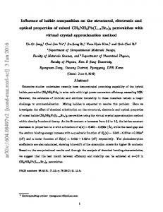


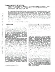


![Ba4[Mn3N6], a Quasi-One-Dimensional Mixed-Valent ... - MDPI](https://m.moam.info/img/260x300/ba4mn3n6-a-quasi-one-dimensional-mixed-valent-mdpi_5b7df8c0097c478d058b4729.jpg)


