RADIOENGINEERING, VOL. 18, NO. 4, DECEMBER 2009
631
Embedded Platform for Automatic Testing and Optimizing of FPGA Based Cryptographic True Random Number Generators Michal VARCHOLA, Miloˇs DRUTAROVSKY´ Dept. of El. and Mmedia Comm., Technical Univ. of Koˇsice, Park Komensk´eho 13, 041 20 Koˇsice, Slovakia
[email protected],
[email protected]
Abstract. This paper deals with an evaluation platform for cryptographic True Random Number Generators (TRNGs) based on the hardware implementation of statistical tests for FPGAs. It was developed in order to provide an automatic tool that helps to speed up the TRNG design process and can provide new insights on the TRNG behavior as it will be shown on a particular example in the paper. It enables to test sufficient statistical properties of various TRNG designs under various working conditions on the fly. Moreover, the tests are suitable to be embedded into cryptographic hardware products in order to recognize TRNG output of weak quality and thus increase its robustness and reliability. Tests are fully compatible with the FIPS 140 standard and are implemented by the VHDL language as an IP-Core for vendor independent FPGAs. A recent Flash based Actel Fusion FPGA was chosen for preliminary experiments. The Actel version of the tests possesses an interface to the Actel’s CoreMP7 softcore processor that is fully compatible with the industry standard ARM7TDMI. Moreover, identical tests suite was implemented to the Xilinx Virtex 2 and 5 in order to compare the performance of the proposed solution with the performance of already published one based on the same FPGAs. It was achieved 25% and 65% greater clock frequency respectively while consuming almost equal resources of the Xilinx FPGAs. On the top of it, the proposed FIPS 140 architecture is capable of processing one random bit per one clock cycle which results in 311.5 Mbps throughput for Virtex 5 FPGA.
Keywords TRNG, on-chip randomness tests, FIPS 140, FPGA
1. Introduction Tremendous growth of the communication systems was significant during last decades. Heavy research efforts in this area have been, and still are, in the development of systems that are more reliable, faster and more power effective. Si-
multaneously, substantial research has been carried out to find suitable security solutions in order to prevent cyberattacks and leakage of confidential or secret information. Modern cryptography [1] provides techniques for successful application of security services. Almost every cryptographic system contains a Random Number Generator (RNG) in order to provide random values for the underlying algorithms. Random Numbers (RNs) are required e.g. as session keys, and therefore they should meet the most strict requirements – they should be unpredictable, uniformly distributed in their range and independent [3]. RNGs can be divided into two main subgroups [4]: Pseudo RNG (PRNG) and True RNG (TRNG). Output of PRNG is mathematically defined and all entropy is given by a random seed. On the other hand, entropy of TRNG is increased by each generated bit. There are several sources of entropy: non-physical (e.g. access time of hard drive, keystrokes, computer mouse movements) and physical (thermal noise, nuclear decay). The most useful is the noise that can be found in electronic platforms such as ASICs (Application Specific Integrated Circuits), MCUs (MicroControllers) and FPGAs (Field Programmable Gate Array). FPGAs are a popular implementation platform for cryptographic systems thanks to their reconfigurability [6]. Weak or obsolete cryptographic protocols or algorithms can be updated easily even in deployed devices. Thus users and devices can resist an attempt of the security treats better. Moreover, entire system should be implemented in the same chip due to security reasons. That is why research on TRNGs especially for the FPGAs is more than a crucial challenge. Survey of the most popular designs was done in [5]. There are the most important designs: TRNG that uses jitter included in the Phase Locked Loop (PLL) output [10], Linear Feedback Shift Registers (LFSRs) where delay element was replaced by an inverter [11], metastability based design [19], and Ring Oscillator (RO) based design [15] with implementation [17], disputes on its principle [18], responses to the disputes [16] and improved implementation [20]. Reliability of [15] is heavily discussed by the world TRNG community and still remains an unanswered question. Although designers make heavy efforts on TRNG im-
´ EMBEDDED PLATFORM FOR AUTOMATIC TESTING AND OPTIMIZING OF FPGA. . . M. VARCHOLA, M. DRUTAROVSKY,
plementation in a robust way in laboratory conditions, their designs are potentially vulnerable to the tolerances of components, technology aging, variations of operating conditions, or attacks in hostile environments [2]. Each of the mentioned disorders could cause degradation of the RNs’ statistical properties and thus weaken an otherwise secure system. The most straightforward way how to detect such a breakdown is to implement a set of basic statistical tests working in real-time as a supplement to the TRNG. Requirements for online tests are listed in [4] – an online test should detect non-tolerable statistical weaknesses, should run fast and consume only little hardware resources. Online tests can be universal or tailored to a particular design. An interesting fact is that authors in proposals of their original designs usually do not consider any methods of online testing that can uncover possible malfunction. Moreover, it will be shown how various modifications during TRNG design can affect its speed or the quality of RNs on a particular example in the paper. The hardware implementation allows us to examine statistical properties of RNs on the fly prior to rigorous analysis by a personal computer using wide spectrum of tests and methodologies e.g. National Institute of Standards and Technology (NIST) 80022 tests suite [22] or Application Notes and Interpretation of the Scheme (AIS) 31 [21] which is recommended for certification of TRNG designs. Once statistical tests are implemented inside an FPGA, there is no need of the fast interface (e.g. as was used in [23]) and high level of design automation is available, hence research work is more effective. The Federal Information Processing Standard (FIPS) 140 [8], [9] randomness tests suite has been chosen among the published statistical tests, which consists of the 4 following tests – Monobit, Poker, Runs, and Long run. Tehe required length of the sequence is 20,000 bits, which implies small demand on hardware resources. Although statistical tests were removed from FIPS 140 recently, they still provide reasonable information on statistical properties of RNs. Nevertheless, relatively small-area implementation of these tests is not trivial. Such hardware implementations of statistical tests Intellectual Property Core (IP-Core) appear in literature rarely; as an example, it is possible to mention [14], where the authors used Virtex 2 FPGA, or [28] where the authors used Virtex 2 and Virtex 5 FPGAs as an implementation platform. However, solution proposed in this paper has significantly better performance while consuming almost the same resources of FPGAs. The paper is organized as follows: Section 2 compares internal and external TRNG testing methods, FIPS 140 statistical tests are introduced in Section 3. Section 4 deals with implementation platform and architecture of the entire system. Section 5 provides insight on analysis and synthesis of the particular tests. Section 6 shows implementation results. Conclusion is given in the last section.
2. Internal and External TRNG Testing Methods There are two main purposes of using randomness tests for TRNGs; the first, testing during process of research, designing and certification and the second, testing when the device is operating in the environment. Both of them have different requirements. The first one uses rigorous analysis mainly on a Personal Computer (PC) with various setups of TRNGs’ parameters and under various working conditions. This is usually a long time process and so design automation can bring time savings and better efficiency of the design progress by reducing human interaction. Design automation can be reached by putting tests inside the device so that the device will manage all the tests itself. Recent research efforts tends to running various TRNG tests or measurements inside the device in order to have instant results or in order not to affect results with external measuring circuitry: [26], [25], [24]. potential treats for TRNGs: frequency injection package temperature core voltage abnormal behavior of the source of randomness deterministic noise interference
PC TESTS
fast interface
FPGA TRNG
Interface
Fig. 1. External TRNG testing setup, where only TRNG and communication interface is implemented in the FPGA device. Tests are processed by PC.
The second purpose requires tests implemented inside the device due to security reasons - to uncover defects of TRNG in the deployed device. The main differences between both architectures are shown in Fig. 1 for external evaluation and Fig. 2 for automated internal evaluation of the RNs quality. potential treats for TRNGs: frequency injection package temperature core voltage abnormal behavior of the source of randomness deterministic noise interference
PC
slow interface
FPGA soft - MCU TRNG Tests IP Core
system bus
632
Interface
Fig. 2. Internal TRNG testing setup, where tests run inside the FPGA device. The result of tests is provided for PC.
RADIOENGINEERING, VOL. 18, NO. 4, DECEMBER 2009
633
The first version of the FIPS 140 standard [8] was introduced in 1994. A particular part of it deals with statistical randomness tests. In 2001 the second version of the document was introduced [9] with slightly changed threshold regions for the Runs test. Here is description of the tests that are included: • T1: The Monobit Test 1. Count the number of ones in the 20, 000 bit stream. Denote this quantity by X. 2. The test is passed if 9, 725 < X < 10, 275. • T2: The Poker Test 1. Divide the 20, 000 bit stream into 5, 000 contiguous 4-bit segments. Count and store the number of occurrences of each of the 16 possible 4-bit values. Denote f (i) the number of each 4-bit value i where 0 ≤ i ≤ 15. 2. Evaluate the following: 15
X = (16/5000) · ( ∑ [ f (i)]2 ) − 5000.
(1)
i=0
3. The test is passed if 2.16 < X < 46.17. • T3: The Runs Test 1. A run is defined as the maximal sequence of consecutive bits of either all ones or all zeros, which is part of the 20, 000 bit sample stream. The incidences of runs (for both consecutive zeros and consecutive ones) of all lengths (≥ 1) in the sample stream should be counted and stored. 2. The test is passed if the number of runs that occur (of lengths 1 through 6) is each within the corresponding interval specified in Tab. 1. This must hold for both the zeros and ones; that is, all 12 counts must lie in the specified interval. For the purpose of this test, runs of greater than 6 are considered to be of length 6. Length of Run 1 2 3 4 5 6+
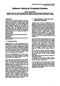
4. Implementation Platform and Architecture of the Implemented System The recent Flash based Actel Fusion FPGA M7AFS600 has been chosen thanks to benefits listed in [12]. The available soft-core ARM7TDMI compatible processor is used for interfacing the tests. Available PLLs are necessary for implementation of a PLL-based TRNG [10], used as a source of RNs under test. This type of TRNG has been chosen only for demonstration of the testing platform based on FIPS 140 tests. A drawback of the Fusion family is unavailability of dedicated multipliers which would be helpful for squaring needed by the Poker test. The proposed IP-Core is written in VHDL and special emphasis was taken on the speed-and-area effective implementation of all tests. The architecture of the entire system is shown in the Fig. 3. There are three main components: the CoreMP7 subsystem, the TRNG with Advanced Peripheral Bus (APB) interface and the FIPS 140 Tests IP-Core with the APB interface. All these components communicate by the APB. There is a direct interconnection between TRNG and FIPS 140 Tests IP-Core that provides random bits for tests. FIPS 140 tests IP-Core consists of APB interface, Control Logic and instances of particular tests. The APB interface translates the results of the tests to the status register of the peripheral, which is possible to be read by software running in the CoreMP7. The Control Logic distribute the synch clk rst
APB Bus
CoreMP7’s APB Interface
result_ready result
Control Logic Monobit Test Poker Test
Tab. 1. FIPS 140 - the Runs Test tresholds, according [9].
• T4: The Long Run Test
2. On the sample of 20, 000 bits, the test is passed if there are NO long runs.
rnd_bit_ready rnd_bit
Test_rdy
Required Interval 2,315 - 2,685 1,114 - 1,386 527 - 723 240 - 384 103 - 209 103 - 209
1. A long run is defined to be a run of length 26 or more (of either zeros or ones).
TRNG with APB Interface
CoreMP7 Subsystem
Test_Result
Runs & Long Run Test
synch
3. Description of FIPS 140 Test Suite
FIPS 140 TESTS IP-CORE
Fig. 3. Architecture of the specialized FIPS 140 IP-Core and its connection to the CoreMP7 subsystem and the TRNG.
634
´ EMBEDDED PLATFORM FOR AUTOMATIC TESTING AND OPTIMIZING OF FPGA. . . M. VARCHOLA, M. DRUTAROVSKY,
signal which indicates end of the 20,000 bits packet and is used for synchronizing and controlling all instances of tests. The Control Logic block also merges the results of all tests into one result.
5. Synthesis of the Particular Tests Each test from the suite is different from the hardware implementation point of view and a specific approach of effective synthesis is needed. This section deals with each test separately.
as Finite State Machines (FSMs). A serial multiplier was used for performing square in order to save logic resources. Its lower speed does not cause complication because there is enough time while 20,000 bits are stored in RAM. A Ripple Carry Adder was used because of the same reason for addition. Finally, the result is tested whether it fits into the interval derived in (2). synch rnd_bit_ready rnd_bit
4-bit Shift Register
A/B Switcher
5.1 Monobit Test The Monobit test is the easiest one within the entire suite. There is only one register necessary that increments its content by one when an input random bit has 0 10 value. The content of the register is compared to the reference threshold values when synch signal is active.
RAM read/ write controller & incrementer
RAM sector A sector B
5.2 Poker Test The Poker test described by equation (1) can be hardly implemented in hardware. That is why a derived compatible equation using integers was used [13] (Appendix A): 15
2
1563175 < ∑ [ f (i)] < 1576929.
Serial Multiplier
Register
Ripple Carry Adder
(2)
i=0
As it is needed to count the appearance of each group of four bits, it is necessary to find the maximum value of [ f (i)] for passing the test in order to allocate the appropriate number of bits for registering. It was shown that if the count of at least one combination of bits exceeds 428 the test would not pass [13] (Appendix B). That is why the architecture needs a 16 · 9-bit register field. The computation of the square and sum takes basically some time and so two such register fields are used; one is used for storing counts of the bit groups and the second is used for performing computations on it. Two times 16 · 9-bits would consumes quite a lot of FPGA resources and so the register field is implemented in the RAM. The data-flow architecture of the poker test is shown in Fig. 4. First of all, a group of 4 bits is collected by the shift register. This value selects the address and the active channel (the A/B switcher output) selects address in the RAM memory. RAM read/write controller and incrementer loads, increments and stores the particular value. There are two sectors in the RAM; while poker data are incremented and stored in the first sector (incoming data), the second sector provides data for the post-processing unit (outgoing data). The roles of both sectors are swapped after 20,000 input bits. Random bits can come with each clock cycle, which implies 4 clock periods for all RAM read/write operations. The control sequence is shown in the Tab. 2. RAM read/write controller & incrementer and the Processing unit are synthesized
Processing Treshold Unit Comparator Poker_ready Poker_result Fig. 4. The data-flow architecture of the implemented Poker test where the RAM read/write controller & incrementer and the Processing unit are synthesized as FSMs.
Clock Period 1 2 3 4
Incoming Data Capture Shift Register Load Poker Value Increment Poker Value Store Poker Value
Outgoing Data Load Data No Operation Clear Data No Operation
Tab. 2. A sequence of RAM read/write operation for the Poker test.
5.3 Runs and Long Run Test The Runs and Long run tests are merged to the same instance due to similar nature of both tests. The test is synthesized as single FSM. The FSM transaction diagram is shown in Fig 5. The FSM consists of the following states: idle, compare, zX, oX; where X in zX and oX states means the number of zeros or ones of particular run, respectively. The FSM
RADIOENGINEERING, VOL. 18, NO. 4, DECEMBER 2009
falls into idle state during reset. After that, random numbers are entered to the FSM in the sequence. When the value of the first random bit is 0 00 , the FSM falls to the z1 state. When the value of the second random bit is 0 00 , the FSM falls to the z2 state. When the value of the second random bit is 0 10 , the FSM falls to the o1 state and the register counting appearance of the run of single 0 00 is incremented, etc. When the state is changed from the right side of the diagram to the left (or vice versa) – that means the run of several same consecutive bits is over – the appropriate register is incremented. In case of this test, register field is stored in the logic for the possibility of incrementing it in a single clock period. The FSM falls to compare state when synch signal is active (at the end of the 20,000 bit sequence) and all registers are tested if their values fit into threshold regions listed in Tab. 1. rst = ’1’
635
of FIPS 140 tests was processed automatically without any need of human interaction, otherwise a designer would be supposed to manage the entire experiment.
6.1 FIPS 140 Implementation Results The VHDL code was synthesized by the Synplify (Actel Version) and the implementation was done by the Designer. Both of them are distributed within the Libero 8.4 which is Actel’s Integrated Design Environment (IDE). Synplify provided the best results (resources consumption and speed) when it was asked for the 110 MHz resulting frequency. Designer was configured for multiple passes (in order to find a better starting position of the placer) with a high-effort place and route algorithm in order to achieve the best results. Results are given in Tab. 3. instance
idle
o1
z1 o2
z2 o3
z3 o4
z4 o5
z5 o6
z6 z26
o26 synch = ’1’ rnd_bit = ’0’
compare
rnd_bit = ’1’
Fig. 5. The state diagram of the FSM of the implemented Runs and Long run test; registered value of particular runs is incremented when transaction from the left side to right one appears (or vice versa).
6. Experimental Results Experimental results of the FIPS 140 IP-Core implementation and results of an experiment on PLL based TRNG [10] are given in this section. This generator was chosen for automatic testing platform demonstration purposes only. Functionality provided by the FIPS 140 IP-Core and CoreMP7 processor allow us to examine the generator output under various values of a certain parameter. Although the value of such parameter is strictly defined by PLL setup and highly recommended by authors, it was changed dynamically while the results of the FIPS 140 tests were observed. A great benefit of this approach is that a big amount
whole monobit poker runs
area (tiles) 1195 91 420 560
M7AFS600 percentage 8,6% 0,7% 4,1% 4,1%
RAM blocks 2 0 2 0
speed (MHz) 116 250 125 125
Tab. 3. Implementation results showing resources consumption and maximum achieved clock frequency.
Authors in [28] have used Xilinx Virtex 2 XC2V10006 and Virtex 5 XC5VLX50T-3 FPGAs for their implementations of FIPS 140 tests. In order to compare the properties of their architectures and the proposed architecture of the tests, codes have been ported to the Xilinx platforms and implemented using Xilinx ISE 10.1 IDE. The only differences to the Actel version are: Xilinx Block RAM memory was used instead of Actel RAM memory and Xilinx DSP48 block was used instead of a serial multiplier. A comparison of the implementation results of the proposed architecture and the results of the architecture published in [28] is shown in Tab. 4. FPGA Implementation LUTs Utilization Max.F[MHz] Max.F/LUTs
XC2V1000-6 Santoro This et. al. paper 626 640 (6%) (6%) 134.7 168.7 0.215 0.264
XC5VLX50T-3 Santoro This et. al. paper 482 492 (1%) (1%) 189.4 311.5 0.393 0.633
Tab. 4. Comparison of the Santoro et. al. [28] FIPS 140 implementation and FIPS 140 implementation proposed in this paper; it was achieved significantly greater maximum clock frequency utilizing almost the same amount of the FPGA resources.
6.2 Basic Description of PLL Based TRNG The basic principle behind the TRNG shown in Fig. 6 is to extract the randomness from the jitter of the clock signals synthesized in the embedded analog PLLs [10]. The jitter is detected by sampling of a reference signal CLJ using a rationally related (clock) signal CLK synthesized in the on-chip analog PLLs with frequencies:
´ EMBEDDED PLATFORM FOR AUTOMATIC TESTING AND OPTIMIZING OF FPGA. . . M. VARCHOLA, M. DRUTAROVSKY,
636
FCLJ
7. Conclusion
MCLJ = FOSC , DCLJ
(3)
MCLK FOSC DCLK
(4)
FCLK =
where FOSC is a reference clock signal and the parameters KM = MCLJ DCLK , KD = DCLJ MCLK are related to the PLL structures. The signal CLJ is sampled into the first D flip-flop using a clock signal with frequency FCLK . There are KD rising edges of CLK signal and 2KM (rising and falling) edges of a CLJ waveform during the time period TQ =
1 = KD TCLK = KM TCLJ R
(5)
where R is the bit-rate of the output TRNG sequence. 50MHz XTAL OSC
PLL PLL
CLJ CLK
D
Q
CLK
D
Q
q(nTCLK )
Decimator (K D )
x(nTQ )
CLK
Fig. 6. Basic structure of implemented PLL based TRNG.
6.3 PLL Based TRNG Results Chosen parameters of PLL based TRNG were: FCLK = 98.750 MHz, FCLJ = 98.387 MHz, MCLJ = 61, MCLK = 79, DCLJ = 31 and DCLK = 20 which results in KD = 2449 and R = 40323 bps. Such generator obviously passed FIPS 140 tests. Although the listed parameters are highly recommended by the authors and the generator provides great robustness, it would be interesting to observe how the decreasing of KD factor can affect statistical properties of random numbers. In order to automate manual work of capturing random data, the proposed FIPS 140 IP-Core implementation for FPGA was used. PLL based TRNG and FIPS 140 tests were controlled by CoreMP7 soft-core processor. The KD constant in VHDL was changed into a register accessible by ARM7. A simple script was run which executes FIPS 140 tests 1000 times for each KD value from 20 to 250. The experiment was ready in 100 minutes’ time. It would be several times more by using traditional approach when tests are running on the PC with great demand on manual work of the designer. The region where FIPS 140 tests began to pass is show in Fig. 7.
An automatic testing and optimization platform was proposed in this paper, based on hardware implementation of the FIPS 140 statistical randomness test suite. This specialized IP-Core can be used as a component of the each cryptographic system where detection of the TRNG malfunction is critical as well. It was shown how is such a FIPS 140 IP-Core practical for research of TRNGs as well. It was performed pretty much of automated tests inside the device without any need of fast interface or human effort of managing the FIPS 140 execution on a PC. The experimental system only sent results to the PC by RS 232 interface. The automated test was controlled by CoreMP7 processor with simple program written in C language. The KD value was observed when the PLL based TRNG began to provide output of better statistical properties. Experiments based on this testing platform can save a lot of research time and provide overview of the behavior of TRNG under various working conditions and under various operating settings. The proposed design can process one random bit per single clock period. The maximum achieved clock period was 116 MHz for the entire tests implemented in Actel FPGA that means it is possible to perform testing of random data with 116 Mbps bit-rate. Whole solution consumes 1195 tiles that is less than 9 % of the popular M7AFS600 FPGA. An alarm can be reported to the CoreMP7 processor which does not need to run FIPS 140 tests anymore and save its computation time for other tasks. Authors in [14] achieved 113 MHz maximum frequency that is comparable with the implementation results in the Actel Fusion FPGA but they used high-performance Virtex 2 FPGA by Xilinx while Fusion is cost-effective Flash FPGA. Authors in [28] used Xilinx Virtex 2 and Virtex 5 FPGAs and so proposed architecture was ported into the same parts in order to compare performance of both solutions. The result was that proposed architecture achieved better performance utilizing the same amount of the FPGA resources. Next research efforts will target deep analysis and optimization of FIPS 140 IP-Core and enhancing it towards AIS 31 criteria [21] in order to be able to implement it in security products. On the other hand, this IP-Core will be used for fast results of numerous experiments on various TRNG principles when changing their parameters or operation conditions or attacking them. Research interests will be focused particularly on the Ring Oscillator based designs [15] and recent principle published in [27].
Acknowledgements This work has been done in Fig. 7. Percentage of FIPS 140 passes regarding to the KD parameter when PLL based TRNG was used.
the frame of the Slovak scientific project KEGA 3/5238/07 of Slovak Ministry of Education an Actel University Program.
RADIOENGINEERING, VOL. 18, NO. 4, DECEMBER 2009
References [1] MENEZES, J. A., OORSCHOT, P. C., VANSTONE, S. A. Handbook of Applied Cryptography. New York: CRC Press, 1997. [Online]. Available at: http://www.cacr.math.uwaterloo.ca/hac/. [2] MARKETTOS, A. T., MOORE, S. W. The frequency injection attack on ring-oscillator-based true random number generators. In Proceedings of Cryptographic Hardware and Embedded Systems. Lausanne (Switzerland), 2009, p. 317 - 331. [3] SCHINDLER, W. Random number generators for cryptographic applications. Cryptographic Engineering. Berlin: Springer, 2009. [4] SCHINDLER, W. Evaluation criteria for physical random number generators. Cryptographic Engineering. Berlin: Springer, 2009. [5] SUNAR, B. Random number generators for cryptography. Cryptographic Engineering. Berlin: Springer, 2009. [6] DAVIES, P. Flexibile security. In Thales e-Security, White Paper Cryptography & Interoperability, 2003. [7] SCHINDLER, W. Efficient online tests for true random number generators. In Proceedings of Cryptographic Hardware and Embedded Systems. Paris (France), 2001, p. 103 - 117. [8] U.S. Department of Commerce / National Institute of Standards and Technology. Federal Information Processing Standards Publication FIPS PUB 140-1, 1994. [9] U.S. Department of Commerce / National Institute of Standards and Technology. Federal Information Processing Standards Publication FIPS PUB 140-2, 2001. ´ M. True random number genera[10] FISCHER, V. DRUTAROVSKY, tor embedded in reconfigurable hardware. In Proceedings of Cryptographic Hardware and Embedded Systems. Redwood City (USA), 2002, p. 415 - 430. ´ J. New methods for digital generation and postprocessing [11] GOLIC, of random data. In IEEE Transactions on Computers, 2006, vol. 55, no. 10, p. 1217 - 1229. ´ M., VARCHOLA, M. Cryptographic system on [12] DRUTAROVSKY, a chip based on actel ARM7 soft-core with embedded true random number generator. In IEEE Workshop on Design and Diagnostics of Electronic Circuits and Systems. Bratislava (Slovakia), 2008, p. 164 - 169. [13] VANCAK, O. Implementation of the Statistical Randomness Tests for Cryptographic Applications in FPGA Devices. Master Thesis. Technical University of Koˇsice, 2009. [14] HASEGAWA, A., KIM, S. J., UMENO, K., KITAMACHI, N. IP core of statistical test suite of FIPS 140-2. Design & Reuse. [Online]. Cited 2009-10-16. Available at: http://www.designreuse.com/articles/7946/ip-core-of-statistical-test-suite-of-fips-1402.html . [15] SUNAR, B., MARTIN, W. J., STINSON, D. R. A provably secure true random number generator with built-in tolerance to active attacks. IEEE Transactions on Computers, 2007, vol. 56, no. 1, p. 109 - 119. [16] SUNAR, B. Response to Dichtl’s Criticism. 2008. [17] SCHELLENKES, D., PRENEEL, B., VERBAUWHEDE, I. FPGA Vendor agnostic true random number generator. In Proceedings of International Conference Field Programmable Logic and Applications. Madrid (Spain), 2006. [18] DICHTL, M. Scrutinizing the assumptions used in the security proof of a true random generator. IEEE Transactions on Computers, 2007. [19] VASYLTSOV, I., HAMBARDZUMYAN, E., KIM, Y. S., KARPINSKYY, B. Fast digital TRNG based on metastable ring oscillator. In Proceedings of Cryptographic Hardware and Embedded Systems. Washington DC (USA), 2008, p. 164 - 180.
637
[20] WOLD, K. TAN, C. H. Analysis and enhancement of random number generator in FPGA based on oscillator rings. In International Conference on Reconfigurable Computing and FPGAs. Cancun (Mexixo), 2008, p. 385 - 390. [21] KILLMANN, W., SCHINDLER, W. Functionality classes and evaluation methodology for true (physical) random number generators. AIS 31: Application Notes and Interpretation of the Scheme (AIS), 2001. [22] RUKHIN, A., et al. A statistical test suit for random and pseudorandom number generators for cryptographic applications. NIST Special Publication 800-22, 2001. ´ M., FOUQUET, R., FIS[23] VARCHOLA, M., DRUTAROVSKY, CHER, V. Hardware platform for testing performance of TRNGs embedded in actel fusion FPGA. In Proceedings of the 18th International Conference Radioelektronika. Prague (Czechia), 2008, p. 145 - 148. [24] ROZIC, V., VERBAUWHEDE, I. Random numbers generation: Investigation of narrow transitions suppression on FPGA. Proceedings of International Conference Field Programmable Logic and Applications. Prague (Czechia), 2009. [25] FISHER, V., BERNARD, F., BOCHARD, N., VARCHOLA, M. Enhancing security of ring oscillator-based RNG implemented in FPGA. In Proceedings of International Conference Field Programmable Logic and Applications. Heidelberg (Germany), 2008, p. 245 - 250. [26] VALTCHANOV, B., AUBERT, A., BERNARD, F., FISCHER, V. Modeling and observing the jitter in ring oscillators implemented in FPGAs. In IEEE Workshop on Design and Diagnostics of Electronic Circuits and Systems. Bratislava (Slovakia), 2008, p. 158 - 163. ´ M. New FPGA based TRNG [27] VARCHOLA, M., DRUTAROVSKY, principle using transition effect with built-in malfunction detection. In International Workshop on Cryptographic Architectures Embedded in Reconfigurable Devices - CryptArchi. Prague (Czechia), 2009, p. 150-155. [28] SANTORO, R., SENTIEYS, O., ROY, S. On-Line monitoring of random number generators for embedded security. In IEEE International Symposium on Circuits and Systems. Taipei (Taiwan), 2009, p. 3050 - 3053.
About Authors. . . Michal VARCHOLA was born in 1984 in Koˇsice. He received his M.Sc. in electronics and telecommunication technologies from Technical University of Koˇsice in 2007. Currently he is a Ph.D student at the Department of Electronics and Multimedia Communications, Technical University of Koˇsice. His research interests include true random number generators for embedded cryptographic applications. ´ was born in 1965 in Preˇsov, SloMiloˇs DRUTAROVSKY vak Republic. He received the M.Sc. degree in radioelectronics and PhD degree in electronics from Technical University of Koˇsice, Slovak Republic, in 1988 and 1995, respectively. He defended his habilitation work - Digital Signal Processors in Digital Signal Processing in 2000. He is currently working as an associated professor at the Department of Electronics and Multimedia Communications, Technical University of Koˇsice. His current research interests include applied cryptography, sensor networks, digital signal processing, and algorithms for embedded cryptographic architectures.
638
´ EMBEDDED PLATFORM FOR AUTOMATIC TESTING AND OPTIMIZING OF FPGA. . . M. VARCHOLA, M. DRUTAROVSKY,
Appendix A
Appendix B
Deriving poker test equation that is possible to implement in FPGA hardware:
Deriving the maximum bit-width for counters used in the Poker test: Let y = f (i)MAX , then the remaining f (i) values would be (5000 − y)/15 and so:
15
X = (16/5000) · ( ∑ [ f (i)]2 ) − 5000
(6)
i=0
where f (i) ∈ 0, 1, ...5000. Test would pass when X ∈ (2.16; 46.17) and so
15
∑ [ f (i)]2 = y2 + 15 · ((5000 − y)/15)2 .
(10)
i=0
Let us examine when (6) will have maximum value x = 46.17:
15
2.16 < (16/5000) · ( ∑ [ f (i)]2 ) − 5000 < 46.17,
(7)
i=0
46.17 = (16/5000) · (y2 + 15 · ((5000 − y)/15)2 ) − 5000. (11)
15
5002.16 < (16/5000) · ( ∑ [ f (i)]2 ) < 5046.17,
(8)
From (11) we can get:
i=0
16y2 + 10000y + 1346078.125 = 0.
vspace2mm 15
1563175 < ∑ [ f (i)]2 < 1576929. i=0
(9)
(12)
There are two roots of (11): y1 = 428.803 and y2 = −196.197, which results in f (i)MAX = 428 .