Energy Efficient Scheduling for Datapath Synthesis Saraju P. Mohanty and N. Ranganathan Department of Computer Science and Engineering Nanomaterial and Nanomanufacturing Research Center University of South Florida Tampa, FL 33620
[email protected] and
[email protected]
Abstract In this paper, we describe two new algorithms for datapath scheduling which aim at energy reduction while maintaining performance. The proposed algorithms, time constrained and resource constrained, utilize the concepts of multiple supply voltage and dynamic clocking for energy minimization. In dynamic clocking, the functional units can be operated at different frequencies depending on the computations occurring within the datapath during a given clock cycle. The strategy is to schedule high energy units, such as the multipliers at lower frequencies such that they can be operated at lower voltages to reduce energy consumption and the low energy units, such as adders at higher frequencies, to compensate for speed. The algorithms have been applied to various high level synthesis benchmark circuits under different time and resource constraints. The experimental results show that for the time constrained algorithm, energy savings in the range of 33−75% are obtained. Similarly, for resource constrained algorithm, under various resource constraints using two supply voltage levels (5.0V, 3.3V ), energy savings in the range of 24 − 53% can be obtained.
1
Introduction
With the increase in demand for personal computing devices and wireless communications equipment, the demand for synthesizing low power consuming circuits has increased. The need for low power synthesis is driven by several factors such as : demand of portable systems (battery life), thermal considerations (cooling and packaging costs), environmental concerns (use of natural resources) and reliability issues. While the first three factors relate to average power dissipation, the last factor is affected by peak power. The power-delay-product has to be minimized to increase battery life, whereas, to increase battery life and reduce delay, the energy-delay-product is minimized.
Let us assume that Cef f , Vdd , f and VT denote the effective switched capacitance, supply voltage, frequency and threshold voltage, respectively. For a CMOS circuit, the energy (E) and power (P ) dissipation per operation and the critical delay (td ) can be described by the fol2 2 , P = Cef f Vdd f and lowing equations : E = Cef f Vdd Vdd td = k (Vdd −VT )γ ; where, γ is a technology dependent factor and k is a constant. From the above three equations, the following can be deduced [2, 11, 10] : by reducing only Vdd , both energy and power can be saved at the cost of performance (speed / time), slowing down CPU by reducing only f will save power but not energy and by scaling frequency and voltage in a coordinated manner, both energy and power can be saved while maintaining performance. This forms the major motivations for our approach. We generate a datapath schedule that will be operated with resources operating at multiple voltages and clocked with dynamic clock. Several approaches have been investigated towards reducing power/energy consumption in both general purpose and special purpose processors. A dynamic voltage scaled microprocessor system is presented in [2], in which the frequency and the voltage levels to be supplied to the processor core, are determined by the help of operating system. A power efficient compiler in [5] determines the voltage level and clock frequency at compilation time for high level code. The authors in [11], describe a system for low-power microprocessor using dynamic voltage scaling. In [4], voltage and clock scheduling algoritms are incorporated in operating system. From the above works, it is quite evident that simultaneous voltage and frequency scaling is becoming important in low power processors. In this work, we aim at incorporating voltage and frequency scaling within the processor itself and develop a scheduling algorithm that can be incorporated into a datapath synthesis tool. Various low power datapath scheduling techniques have been reported in the literature. A profile driven synthesis system is introduced in [8] which minimizes switching capacitance. A scheduling algorithm called Multiple Operating Voltage Energy Reduction is presented in [6],
Cycle2
tm
*
Cycle1
+
*
V
tm V V
Em Em Ea
t+m
-
V
tm V V-
-
Em Em -
Ea
Datapath
Controller
(FU1, V1)
Storage Unit ( for cfic )
en
Mux−Reg
cfic
Single Frequency Dynamic Frequency
(FUi, Vi) en
Internal Bus en
tm V
Ea
(a) (b)
(c)
V
Ea
(d) (e)
(f)
ta
Dynamic Clocking Unit (DCU)
fbase
Cycle3
+
Mux−Reg
fbase
cfi c
fc
1 Clock to 2 all FUs i n−1 n
Mux−Reg (FUn, Vn)
i = 1, 2, .......n
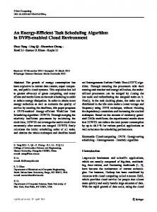
Figure 1. Example data flow graph (DFG) Figure 2. Processor Model which uses ILP formulations. A dynamic programming technique for multiple supply voltage scheduling is discussed in [3]. A time constrained multiple voltage scheduling technique is proposed in [13]. A resource constrained scheduling algorithm with multiple supply voltages is given in [7] which helps in reducing power using multiple supply voltages. In [14], a resource and a latency constrained listbased scheduling algorithms with multiple supply voltages are discussed. A resource and a time constrained scheduling algorithms are described [9] which uses the Lagrange multiplier method. The above scheduling techniques are based on a single clock frequency and consider multiple supply voltages, voltage scaling, capacitance reduction, and switching activity reduction. In this work, we consider the use of dynamic frequency clocking (DFC) alongwith multiple supply voltage in developing resource / time constrained low power datapath synthesis schedulers. We propose two new datapath scheduling algorithms, one is called RC-DFC (resource constrained) and other is called TC-DFC (time constrained), which aim at reducing energy consumption.
2
Dynamic Clocking and Energy Savings
In dynamic frequency clocking [1, 12], the clock frequency is varied on-the-fly based on the functional units active in that cycle. In this clocking scheme, all the units are clocked by a single clock line which switches at run-time. The dynamic clocking unit (DCU) generates the required clock frequency uses a clock divider strategy to generate frequency which are submultiples of the base frequency. Base frequency fbase is the maximum frequency (or multiple of maximum) of any functional unit (FU) at the maximum supply voltage. As discussed in the previous section, frequency scaling helps in reducing power, but not energy [2]. The frequency reduction creates an opportunity to operate the different functional units at different voltages, which in turn, helps in energy reduction. Let us consider the DFG shown in Fig. 1 scheduled to three control steps. Let ta and tm be the delays of the adder and the multiplier respectively at the maximum
supply voltage V . Let us consider, operation of this DFG in three possible modes as follows. (i)Single supply voltage and single frequency : Each cycle has clock width dictated by the slowest operator delay tm . The total energy consumption is given by ES = 2Em +2Ea and the total delay is TS = 3tm . − (ii)Multiple supply voltage and single frequency : Let, Em and Ea− are some energy values less than Em and Ea respectively and t+ m be the delay of multiplier at lower voltage V − . The energy consumption of the DFG is given by − + Ea− . In this case, the total delay E M = E m + Ea + Em + is, TM = 3tm . Since, EM < ES , but TM > TS , it means that the energy savings comes at the cost of time penalty. In this case, energy consumption of the level converters is to be taken into account. (iii)Multiple supply voltage and dynamic frequency : Say, we fix the clock cycle width for the 3rd cycle at ta which is smaller than tm ; this allows us to increase the clock width of some other cycles from tm to some t+ m without violating the time constraints. In this case, the total delay is TD = t+ m + tm + ta and the energy consumption is EM (same as, case (ii)). Since, TD ≤ TM , TD ≈ TS and EM < ES , energy reduction is achieved without degrading performance. In this case, energy overhead of level converters and DCU is to be considered. The processor model consists of a datapath, a controller and a DCU as shown in Fig. 2. The datapath consists of n functional units (FUs) with registers (Reg) and multiplexors (Mux). A controller decides which FUs are active in each control step and those that are not active are disabled using the Mux. The controller has a storage unit to store the parameters cf ic obtained from the scheduling. The cycle frequency fc is generated dynamically and a FU operating at one of the supply voltages (5.0V, 3.3V or2.4V ) is activated. Level converters are used when a low-voltage FU is driving a high-voltage FU. The delay of a control step is dependent on the delays of the FU, Mux and Reg pairs. The worst case delay of a control step can be written as : dc = Regdelay + M uxdelay + F U delay + levelconverterdelay, where, dc is the delay
Table 1. Delay values for 16-bit components Library Component Register Register Multiplexor add/sub Multiplier
Delay Type set-up propagation propagation propagation propagation
Delay (5V) 3.3ns 3.3ns 6.0ns 15.4ns 43.7ns
Delay (3.3V) 5.9ns 5.9ns 10.8ns 27.8ns 78.9ns
Delay (2.4V) 10.1ns 10.1ns 18.4ns 47.3ns 134.2ns
Table 3. Energy dissipation in level converters V1-V2 2.4V 3.3V 5.0V
2.4V 21.53 22.5
3.3V 53.04 61.4
5.0V 139.4 178.1 -
Table 4. Delays and operating frequencies Table 2. Energy dissipation of functional units Library Component Mux add/sub Multiplier
Energy (5V ) 9pJ 57pJ 2202pJ
Energy (3.3V ) 4pJ 25pJ 960pJ
Energy (2.4V ) 2pJ 13pJ 507pJ
of control step c, the register delays include the set-up and propagation delays, and FU delay is the delay of the slowest FU in the control step c. The estimated worst case delays of the library components are shown in Table 1. The worst case delay of a level converter is less than 1ns as seen from HSPICE simulations. Assuming a switching activity of 0.5 at the inputs, the average energy dissipation for the components such as, the adder/sub, multiplier, etc. are estimated for different voltage levels as shown in Table 2 and 3. Table 4 shows the clock frequencies corresponding to the use of each FU at different voltages. For a given base frequency (fbase ), maximum frequencies of each FU base is scaled down to operating frequencies given by ( fcf ic ), where, cf ic = 1, 2, ..., anynaturalnumber. The value of cf ic is bounded by the product of the total number of resource types and number of voltage levels. The possible frequencies are, ALUHigh (cf ic = 1), ALUM ed (cf ic = 2), ALULow (cf ic = 4), M U LTHigh (cf ic = 2), M U LTM ed (cf ic = 4) and M U LTLow (cf ic = 8).
3
TC-DFC Scheduler
The datapath is represented in the form of a DFG constructed as a sequencing graph. Fig. 3 shows such a graph for the HAL benchmark. The inputs to the algorithm are an unscheduled DFG, the scaled down operating frequencies, and the execution time constraint Tc for the whole schedule. To get more energy savings and at the same time maintain performance, the multipliers are to be operated at as low frequencies as possible and the adders at as high frequencies as possible. This objective can be achieved if adders / subtractors are not operated alongwith multipliers in the same duty cycle. In cases, when they are to be operated during the same cycle to meet the time constraint, energy savings will come from the multipliers only. Initially, TC-DFC generates a schedule such that the low frequency operators are
Library Components add/sub/comp. (ALU) Maximum Frequencies Operating Frequencies Multiplier (MULT) Maximum Frequencies Operating Frequencies
Delays and Frequencies 5.0V 3.3V 2.4V 25.7ns 45.5ns 76.8ns 38.91M Hz 21.97M Hz 13.02M Hz 36M Hz 18M Hz 9M Hz 54.0ns 96.6ns 163.7ns 18.51M Hz 10.35M Hz 6.1M Hz 18M Hz 9M Hz 4.5M Hz
scheduled at earlier steps and the high frequency operators are scheduled at later steps. Later on, the TC-DFC modifies the schedule by moving operations from one step to another with the objective of meeting the time constraint. Cycles c=0
Source
NOP v0
c=1
*
v1
c=2
v2
*
*
*
v3
v8
v7
+
1
v9 2
v10
+
1
2
−
*
1
2
c=3
v6
*
1
1