that is in the clock cone and can be propagated only to a clock port is called a clock fault. In modern design, a clock cone is often gated with other enable logic ...
Enhanced Testing of Clock Faults Teresa L. McLaurin, Richard Slobodnik ARM Inc. 1250 S. Capital of TX Hwy, Bldg 3, Ste 560 Austin, TX 78746, USAWilsonville, Abstract A test methodology for the control signals including clock logic, ripple reset and register file read/write control of the Cortex-A8TM high performance microprocessor core is presented. The target fault models include the stuck-at fault, transition fault and hold time fault models.
1. Introduction ARM’s main DFT goals, for the Cortex-A8TM core, were high test coverage of all logic and RAMs, creating an example test methodology that would not be too complex, so that it could be easily disseminated to ARM customers, and finding 3rd party tools that would work on the design. It is always important to keep the costs low and the timing impact to the functional design to a minimum. In addition, test compression and power, during test, had to be considered. There are numerous test structures on the Cortex-A8TM microprocessor core [1] which required special attention. The structures of concern were the custom latch-based small arrays, the non-scan register files, the reset logic, modular test compression, power during test and clock gating structures. The ATPG tools were already able to handle some of these structures, but for others had to be enhanced. The clock control logic is a crucial part of the logic that must be tested to ensure the correctness of the design and meet the speed requirement of the Cortex-A8 processor and other designs. To satisfy power constraints during both system mode and test mode, the modern design is often partitioned into smaller clock domains, which limits the number of active domains and this bounds the maximum power consumption [1], [2]. Test clocks and control are often derived from a PLL for at-speed structural testing [3], [4]. In a high performance design a PLL will deliver at-speed capture clocks[1], [5]. It brings several advantages to system performance and reliability, such as reduced transistor count, higher speed and testability. Another example of clock control logic is used by many small non-scan register files around the design. These design practices are implemented by sophisticated clock control logic and create a great challenge for DFT engineers to achieve high quality test goals while maintain-
Kun-Han Tsai, Ana Keim Mentor Graphics Corporation 8005 S.W. Boeckman Road OR 97070, USA ing low test cost. Ensuring that the control logic is tested properly is the focus of this paper. The transition fault model is one of most commonly used fault models for the scan-based at-speed test [6]. It is a pin-based fault model which assumes that a gross delay is located in one pin or one net, and the delay is longer than the slack of any combinational path. The advantage of the transition delay fault model is that the number of faulty sites is linear to the design size and can be created automatically by an ATPG tool. The major limitation of the model is that there is no guarantee that the fault to be tested is in a long (critical) path, thus the pattern may not detect small delay defects or a delay caused by multiple pins. The path delay fault model [7] is another at-speed test fault model, and it is designed to explicitly target user-specified paths. The path delay fault model allows user to target the paths on the performance critical area that are not covered by the transition fault model. However, the number of paths in a design is extremely large and to target just performance critical areas may not be possible and still fit into the test cost model. Recently, an enhanced transition fault model, called timing-aware ATPG, was proposed to overcome the limitation of existing at-speed test fault models [8]. The method is based on the transition fault model with pinbased fault location, and use the circuit timing to ensure the faults are observed through long paths. On the other hand, both the transition fault model and the path delay fault model target only the faults causing a setup time violation, i.e. the faulty effect causes an extra delay on a data path. When a fault happens on the clock control logic, it can cause either a setup time violation, a hold time violation or both. It is necessary to cover hold time faults as well as setup time faults to ensure the correctness of the control logic. Three hold time fault models were introduced in [9] to target short data paths and two propagation conditions are introduced, i.e. robust and nonrobust conditions. In [10], the author proposed a pathbased approach for the hold time fault and perform pathbased test pattern generation. There are two limitations for the proposed path-based method. First, it requires that targeted paths are explicitly specified like the path delay fault model. Second, the proposed pattern transformation may not work when the source and sink flops are controlled by different clock gating logic as explained in section 4.3.
Paper 31.2 INTERNATIONAL TEST CONFERENCE 1-4244-1128-9/07/$25.00 © 2007 IEEE
1
In this paper, we will explain how the clock fault can be modeled by both the hold time fault model and the transition fault model in data paths. In addition, the test generation method for the setup time faults as well as the hold time faults on the clock cone are presented. The proposed hold-time fault model is not based on paths. Instead, a pair of combinationally connected source and sink cells in the same clock domain is used to define a hold time fault. The proposed method bounds the hold time fault population and can be created automatically. The rest of this paper is organized as follows. Section 2 will describe the control logic used by ARM Cortex-A8TM microprocessor core. Section 3 discusses how the static faults on a clock cone are tested. Timing fault testing, including faults causing either setup time or hold time violations, will be explained in section 4. Section 5 shows the statistics of control faults in the core and demonstrates the effectiveness of the test strategy, followed by conclusions and future work.
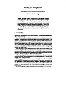
CSDFF F u n c tio n a l in p u t C lo ck G a te D Q g clk
E n a b le
E N
CLK SE
S c a n in p u t s clk
D
Q
EN
D
SI
Q
SI SO EN
SO
EN
Figure 2: CSDFF with clock gate
This section describes the control logic that is used by ARM Cortex-A8 processor.
Though the csdff required both a functional clock and a shift clock, only the functional clock and a scan enable were routed to the clock gate of the csdff. The generation of the scan clock locally eliminates the need to route the scan clock across the core. In addition, the Cortex-A8 processor has custom logic which is latch-based, controlled by clock gates and mainly non-scan. These customs usually contained RAMs or register files. Enhancements to the ATPG tool had to be made in order to get coverage on this logic (see section 3.3). The ATPG tool is able to handle the two different types of flip-flops (csdff and Muxd) with their clock gates as if the entire core were MuxD.
2.1.
2.2.
2. Sequential Cell Control Logic for ARM Core
Scan Cell Clocking and Clock Gating Scheme
The Cortex-A8 processor contains two types of scan cells; MuxD and clocked scan cells. MuxD type scan flop is shown in Figure 1 and has a single clock connected to it. During implementation, clock gating is added to reduce power during functional operation. An enable override, controlled by scan enable (SE), is required to ensure safe shift (see Figure 1). Clock gates typically control numerous sequential elements.
Ripple Reset Logic
The Cortex-A8 processor utilizes an asynchronously asserted and synchronously de-asserted reset. In addition, the core contains repeater flip-flops after the synchronizer to allow the reset de-assertion to occur at functional speed. The design of the reset logic is shown in Figure 3.
Unit To resettable FFs D
Reset Synchronizer
Q
SI D
MuxD Flipflop
D
Q
Q
Reset
Q
R
SI
SI
D
reset repeater
R
R
SI R
Q
Unit
SE
Clock Gate
To resettable FFs D
SE
D
Enable Logic
R
gclk
reset repeater
EN
Unit SE
ClK
Q
SI
Q
SE = Scan Enable gclk = gated clock
To resettable FFs D
Q
Unit
SI
To resettable FFs
R
Figure 1: MuxD Flipflop with clock gate
D
reset repeater
Q
SI R
reset repeater
The clocked scan cell (csdff), shown in Figure 2, contains three latches. It required a different type of clock gate (also shown in Figure 2) as the csdff requires a scan clock (sclk) and a functional clock (gclk) to operate properly. However, this removes the need for a multiplexer in the functional data path.
Paper 31.2
Figure 3: Reset Structure
Only the reset repeater flops required gating to ensure safe shift as shown in Figure 4a. Scan enable was employed to gate the reset signal that output from the repeater flops and connected to the asynchronously reset
INTERNATIONAL TEST CONFERENCE
2
flops. The reset output from the repeater flop was disabled during shift, but allowed to toggle during capture cycles. This allowed two things that were not available in previous designs, which utilized a multiplexer to gate the reset out of the repeater flops (shown in Figure 4b). First, the wire between the reset repeater and the SE gate is testable (see Figure 4a). Second, the path between the reset repeater flop and the asynchronously reset flop is able to be tested at speed during structural testing.
SET
CLR
To active low asynchronous reset ports of FFs
Q
b) O ld Test Structure R eset repeater From reset register 0 D synchronizer Q 1 Scan input S ET
S can enable R eset
CLR
Q
0
To active low asynchronous reset ports of FF s
1
TESTM O D E
Figure 4: Reset Test Structures
The ATPG tool now has the capability to understand this logic and to test it properly without adding any constraints. 2.3.
Register File Control Logic
The Cortex-A8 processor instantiates two register files that were not MBIST tested or scan inserted. Scan insertion was initially applied, but was removed since the register file storage is implemented as a phi-2 (clock low open) latch in a custom implementation [1]. A synthesizable register file is capable of full scan, but the custom implementation was utilized to meet higher functional frequency targets. The register file has multiple read and write ports and was modeled as a multi-port latch in the ATPG tool like the type shown in Figure 5. The tool initially could not detect the clock faults as it did not recognize the device as a register file. The ATPG tool viewed the phi-2 latches as non-scan and transparent. Although the ATPG tool was capable of testing through the register files, numerous phi2 latch clock faults were not detected, resulting in lower overall test coverage.
Paper 31.2
c lk 1
w r it e p o r t 2 c lk 2
Figure 5: Multiport Latch
a) N ew Test S tructure R eset repeater From reset register 0 D synchronizer Q 1 S can input S can enable R eset
M u lt ip o r t L a t c h w r it e p o r t 1
The ARM register file is built with latches with multiple clock ports. However, the ATPG tool did not leverage the additional clock ports to set up deterministic capture of the stuck-off clock faults. If data is written to write port 1 of this latch followed by a write of databar to write port 2, the good machine value of databar would be output. However, a bad machine value of data on the subsequent read indicates that port 2 has a write clock stuck-off fault. Although, the ATPG patterns were performing such sequences, the clock stuck-off fault was not detected. An enhancement to the ATPG tool was made to understand the multiport structure such that fault credit was attained (see Section 3.3).
3. Static Fault Test Generation for Clock Cone 3.1.
Definitions
Definition 1 a clock cone is the combinational fanin cone of a clock port or an asynchronous set/reset port. A fault that is in the clock cone and can be propagated only to a clock port is called a clock fault. In modern design, a clock cone is often gated with other enable logic for various purposes such as the power reduction. The clock cone is further classified by two parts: a clock propagation cone and a clock enable cone as defined below. Definition 2 a clock propagation cone is the intersection of a clock pin fanout and fanin of a clock port of an edgetrigger flip-flop (referred to as flop) or a level-sensitive latch (referred to as latch). A fault inside the clock propagation cone is called a clock line fault. Definition 3 a clock enable cone is the combinational fanin cone of a clock port that is outside the clock propagation cone. A fault inside the clock enable fault cone is called a clock enable fault. Figure 6 shows an example of a clock cone which contains a clock propagation cone and a clock enable cone. One major difference between a clock enable fault site and a clock line fault site is the waveform when a clock is pulsed. Only the waveform of a clock line fault site can also pulse. The waveform of a clock enable fault site is either a constant value or a rising or falling transition. Note
INTERNATIONAL TEST CONFERENCE
3
that it is important to distinguish the clock enable fault from the clock line fault for ATPG purposes. This is because the fault activation conditions are different between these two types of faults. In addition, the test strategy for a clock line fault and a clock enable fault is also different, which will be explained in Section 3.2. FF1 D Q
LA1 D Q
CK
CK
FF3 D Q CK
clock cone
CLK CK
CK
D Q FF2
D Q LA2
clock propagation cone clock enable cone
@act
x
CK
D Q LA3
Figure 6: Clock cone definition
Note that set and reset ports are optional ports on a latch or flop. If they exist, they are treated as a level-sensitive clock ports and the same definitions above are applied to set or reset ports. A latch or flop can contain multiple clock ports. Each clock port would control one data port. Definition 4 a stuck-at-active fault, denoted as @act, (a stuck-at-inactive fault, denoted as @act) is a fault in a clock propagation cone for which the faulty value will incorrectly activate or inactivate a level-sensitive clock port (a latch clock for example). Only a level-sensitive clock port contains a stuck-at-active fault. A stuck-at fault is always a stuck-at-inactive fault for an edge-triggered port, since the faulty value prevents any transition edge. Definition 5 a stuck-at-enable fault, denoted as @en, (a stuck-at-disable fault, denoted as @en) is a fault in a clock enable cone for which a faulty value will enable or disable the clock port. The control signals of a RAM include read control and write control and are treated as clocks. Both read control and write control can be either level-sensitive or edge-triggered. A RAM gate can contain multiple read and write ports. Each of them is associated with one read/write control and an optional read/write enable. Set and reset are also optional control signals to a RAM [12]. 3.2.
Clock Fault Detection Strategy
There are three reasons to separate clock faults from the rest of the fault population. First, to ensure the highest test quality, any fault in the clock cone that may cause a malfunction should be detected. Even though the percentage of clock cone faults may be small, any fault in the clock line is likely critical to the correctness of the function. Second, the common fault models are not adequate for achieving high fault coverage on clock fault models. Figure 6 shows an example of a stuck-at inactive fault (LA3/ck @act) that cannot be detected directly using the stuck-at model. This is
Paper 31.2
due to the fact that there is no way to initialize latch LA3 in the faulty machine. On the other hand, using the concept of detected-by-implication (DI) as explained later in section 3.3, the fault can be ensured covered when certain data faults are detected. In addition, the clock transition fault is not tested by directly using the transition fault model. The slow to transition on a clock fault may cause either a hold time violation, a setup time violation or both. Section 4 explains how to test the slow transition fault on the clock cone. The final reason, to separate clock faults from the rest of the fault population, is for test pattern reduction. Since many clock faults are detected by implication, they do not need to be targeted explicitly. This reduces both test volume and ATPG effort. 3.3.
Detected by Implication (DI)
One commonly used test technique in the ATPG tool is called implication detection [11]. One example of implication detection is the fault related to the scan operation. If the chain test patterns of toggling 00 and 11 are applied to ensure the correctness of the scan chain operation, then the static faults along the scan path and the clock fault causing an incorrect scan operation will be detected. Those faults are marked as detected by implication (DI) once the scan cells are identified, so the ATPG engine does not need to explicitly target them. This technique allows the ATPG engine to exclude the faults that have been covered and allows it to focus on necessary faults to improve the test quality and reduce pattern count. The implication detection concept can be applied to the clock lines for a non-scan cell. When a single-port edgetriggered flop output stuck-at-1 fault is tested by pattern p, (and stuck-at-0 is detected by p’) the stuck-at-inactive faults at the clock ports of the flop should also be detected by either p (or p’). This means that the clock fault will cause the pattern p to fail on the tester. Note that this is true only if the flop output fault is not initialized by an asynchronous set/reset port in pattern p. Similar reasoning can be applied to the stuck-at-inactive fault for the clock port on non-scan level-sensitive latches. Without using implication detection the stuck-at-inactive fault can only be a potential detect for the single port flop/latch without set and reset ports. This is because the faulty machine value is unknown and there is no way to initialize the faulty flop/ latch to a known value. The process of implication detection is very fast since it needs to check only the fault detection status of sequential element output faults without any simulation effort. For the clock @act faults on a multipleport latch or a latch with a set/reset port, the output fault cannot be used to derive a DI fault unless the simulation data is available to check which clock port is used to detect the output faults. For this type of a cell with multiple-ports or set/reset ports, the data line fault can be used. When data line stuck-at-0 and stuck-at-1 faults are both detected, the
INTERNATIONAL TEST CONFERENCE
4
corresponding clock port @act fault is detected by implication. Table I summarizes the different clock fault types and the test strategy. For @act faults on scan cell, they are detected by implication through the scan tracing, denoted as DIs, when the chain test pattern is applied. For @act faults on a non-scan cell and on a RAM read/write control, the DI faults are derived after the faults on the data or output port are detected explicitly by ATPG, which is denoted as DId. Table I: Static control fault category and test strategy clock line fault clock enable fault gate type @act @act @en @en @ATPG scan flop n/a DIs DIs @ATPG @ATPG latch DIs DIs @ATPG nonflop n/a DId DId scan @ATPG @ATPG latch DId DId @ATPG DId e-read n/a DId @ATPG R e-write n/a DId DId @ATPG @ATPG A l-read DId DId @ATPG @ATPG M l-write DId DId e-read (write): edge-trigger read (write) port l-read (write): level-sensitive read (write) port @ATPG: targeted by stuck-at ATPG engine DIs: detected-by-implication through scan DId: detected-by-implication through data and output faults
3.4.
Stuck-at ATPG (@ATPG)
Detected-by-implication does not help for a stuck-atactive fault, so it needs to be detected explicitly using ATPG. A two cycle test pattern is shown in Figure 7 to illustrate the detection of a stuck-at-active fault. The first cycle initializes the latch and the second cycle forces the data input of the latch to the opposite value while forcing the clock port LA1/EN off. This activates the faulty effect of (1/0) at LA1/Q in the second cycle. The faulty effect is propagated in the same cycle to an observation point, which is LA2 in this example. The good/faulty value of LA2/Q is 1/0 when CLK2 is pulsed in the second cycle and thus captures the faulty effect. LA1
D
LA2
D Q
@act
CLK1 x
EN
D Q
I1 CLK2
EN
CLK1 CLK2 LA1/D I1
1/0
3.5.
Ripple Reset Logic
The testing of a static fault on the reset logic described in Section 2.2 is similar to the testing of a clock cone fault. Implication detection is applied to stuck-at-active faults for the pin directly driving the reset port, if the cell is scanned. If it is a non-scan cell, the stuck-at-active reset fault can be implied whenever stuck-at-0 is detected on the Q output of the cell. The reason for this is that to detect a stuck-at-0 at Q, the good machine value detection of a stuck-at-0 fault on the Q requires that ATPG sets the Q to a “1” which in turn implies detection of the reset stuck-on fault for the non scan cell. Detection of a stuck-at-inactive fault on the reset port is detected by loading a 1 to the cell and asserting the reset signal to propagate the good/faulty effect to a downstream observation point.
4. Timing Fault Test Generation for Clock Cone Definition 6 a slow-to-active fault, denoted as s↑, (a slowto-inactive fault, denoted as s↓) is a fault in a clock cone which faulty value will cause extra delay to activate or inactivate the clock port. The timing fault on clock cones can cause either a setup time violation, a hold time violation or both. The first principle of detecting an at-speed fault is still using the detected-by-implication scheme as explained in section 4.1. Most scan path faults and clock propagation cone faults are covered by the DI scheme. On the other hand, the clock enable faults are not covered by implication detection because when testing at-speed faults on a data path, the tool prefers to justify the clock enable line to be a constant value. So, the slow transition on a clock enable line needs to be targeted explicitly to activate the transition at the clock enable line. When the fault is activated, it triggers the slow edge at the clock port, and the faulty effect is only observable when there is transition on data path. For a slow-to-active fault, the faulty clock port triggers a transition on the faulty flop/latch which causes a slow transition at the flop output. The setup time violation can be observed by a downstream flop/latch in the following cycle assuming that the delay on the clock is longer than the slack of the propagation path. This type of detection approach is explained in section 4.2 and is needed for the type of logic shown in Figure 1 and Figure 2. When there is a transition at the data port of the faulty flop/latch, the slow clock port will cause a hold time violation and capture the new value, after the transition, if the clock port delay is longer than the upstream path from where the transition is propagated. The hold time detection method is described in section 4.3. Note that the method we use does not include delay data information (e.g. Standard Delay Format). It is assumed that when the fault is observed, the delay of the fault is always larger than the slack of the fault propagation path to capture the faulty effect.
Figure 7: Detecting @act fault of a non-scan latch
Paper 31.2
INTERNATIONAL TEST CONFERENCE
5
4.1.
Detected by Implication for Transition faults
When applying implication detection through the scan tracing for an at-speed fault type, it needs to be done carefully so that at-speed faults are not skipped and just covered by the scan operation which is typically operated at a slower speed. Figure 8 indicates the region of DIs for the transition fault type which are indicated by the bold lines. Only the faults that are directly observable through scan chain paths are marked as DI because these paths are intended to function only at the scan speed. The scan_in pin and the branch of the scan_in pin driving the system logic is not considered to be in the DIs region because the scan_in pin could be shared with a functional pin and may need to be tested at a higher frequency. Similarly, the output port of the last scan cell (FFn/Q) to the scan_out pin is not in the DIs class because the path could be used in the functional mode and may need to be tested at higher frequency.
FF1 D SI
FF2
Q CK
D SI
FFn
Q CK
D SI
Q
scan_out
CK
scan_enable
DIs paths
scan_clock
Figure 8: DIs for the transition fault type
For the DId type implication, a similar reasoning as the stuck-at fault on the data input and flop/latch output can be applied to learn the clock line slow-to-active faults. On the other hand, the clock enable slow-to-active faults cannot be implied directly since there is no guarantee that a slow-toactive transition happens at the clock enable line when detecting the corresponding data line faults or cell output faults. 4.2.
At-Speed Fault Testing - Setup Time Violation
Figure 9 shows an example of detecting a slow-toactive fault on a clock enable cone, (LA1/Q, s↑). The example logic contains two clock enable gates that drive the clock ports of the scan flops FF1 and FF2, as shown by the shadowed area of Figure 9. The clock gates are controlled by the scan flops FF3 and FF4. To activate the fault, a value 0 is loaded to FF3 and a 1 is justified at FF3/D in the first cycle. This creates a rising transition at FF3/Q at the leading edge of the first clock pulse. Since the clock gate is guarded by the active low latch LA1, the rising transition at the faulty site LA1/Q is delayed after the trailing edge of the first clock pulse. Once the fault is activated at LA1/Q, the rest of ATPG job is equivalent to the detection of a transition fault at the output of FF1, either slow-to-rise or slowto-fall fault, In this example, a slow-to-rise fault is used to demonstrate the method. So, a rising transition is triggered
Paper 31.2
1
FF3 D 0 Q
1 LA1 D Q
s↑x
CK
I1
FF1 D 0 Q ck
1 FF4 D 1 Q
I2 LA2 D Q
I3
FF2 D 1/0 Q ck
CK
CLK CLK FF3/Q LA1/Q FF1/Q FF2/Q
Figure 9: Detecting clock enable slow-to-active fault (LA1/Q, s↑) by using transition fault (LA1/Q, s↑) with an extra condition FF1/Q rising transition at the 1st cycle
system logic scan_in
at FF1/Q in the second cycle and the faulty effect is propagated and captured by FF2 at the third cycle.
Similarly, a slow-to-inactive fault on the clock enable cone of a flop can be activated after the trailing edge of the first CLK pulse. Take (LA1/Q, s↓) in Figure 9 as an example. By loading FF3 with 1 and justifying FF3/D as 0, the fault (a falling transition) will be activated after the first clock pulse. When pulsing CLK at the second cycle, FF1/ck is not triggered for the good machine, thus FF1/Q remains the same value as the first cycle. For the faulty machine, since the falling transition at LA1/Q arrives late, CLK pulse will propagate to FF1/ck and cause FF1 to capture a new value. Therefore, the faulty effect can be captured at the faulty pin’s driving flop FF1 by justifying that FF1/Q and FF1/D are different values while pulsing CLK at the second cycle. The other part of the control logic, to be targeted by the transition fault model, is the reset logic shown earlier in Figure 3. Since the ripple reset logic needs to function atspeed, these faults are also targeted by the transition fault model. Figure 10 depicts how to detect slow-to-rise fault (FF2/clr, s↑) at the reset port using the transition fault model. A slow-to-active fault is detected by loading a 0 into the flop FF1 and justify 1 at FF1/D for the first capture cycle. This creates a rising transition at the reset port when the clock is pulsed. In the same cycle, FF2 is loaded with value 1, so that when the rising transition arrives at the reset fault of FF2, it creates a falling transition at FF2/Q. The falling transition is propagated and captured by the downstream flop FF3 when the second clock is pulsed.
INTERNATIONAL TEST CONFERENCE
6
SE
0
(FF2/clr, s↑) FF2 clr
x
FF1
1
0
D
Q
D
CK
Q CK 1
that this example also indicates that the hold time faulty effect should be launched and captured by the same cycle. In contrast, the setup time faulty effect is typically captured one cycle after the launch cycle.
FF3 D
Q
0/1
CK
CLK
CLK CLK
1
FF2/Q
FF2/D
FF3/D
FF2/Q
FF3/Q
Figure 10: Test for a reset port slow-to-active fault
FF2 0
D
FF2/CK
FF2/clr
4.3.
FF1
FF1/Q
D
Q CK
(FF1,↑,FF2)
Q
0/1
CK
x (FF2/CK, s↑)
CLK
Figure 11: Transition fault (FF2/CK, s↑) at clock line is modeled as a hold time fault (FF1,↑,FF2)
At-Speed Fault Testing - Hold Time Violation
A hold time fault can be caused by either a short data line (e.g. data line speed-up), or a slow clock line on the sink cell. The basic hold time fault is modeled by a pair of sequential cells and a transition function, which is either a rising or a falling transition. The fault causing a hold time violation on a scan flop can be observed by the chain test pattern, so DIs scheme is applied for the hold time faults on scan flops as an initial step to cover the hold time faults on the scan cells. Nonscan cells need to be considered explicitly by the ATPG engine. In [9], the authors proposed three hold time fault models (i.e. F1, F2 and F3). The difference between the fault models are the time and the location when the faulty effect happens. The model F2 is used here, which assumes that only a sink flop’s clock port receives the clock edge late. The rest of clock ports receive the edge on time. This model requires that the faulty effect is propagated after the capture clock pulse. Definition 7 a hold time fault is denoted as a triplet (Rs, tr, Rd), where Rs is the source cell, tr is the transition type at the source cell and Rd is the sink cell where the faulty effect is captured. tr is either a rising transition, denoted as ↑, or a falling transition, denoted as ↓. The fault (Rs, tr, Rd) will cause the Rd cell to receive the new value after the transition at the Rs output is triggered by a clock pulse. Figure 11 shows an example of a clock port slow-toactive fault, which can be modeled as a hold time fault. Assume that FF1 is a scan cell with a loaded value of 0, and FF1/D is a 1 at the beginning of the capture cycle. When the clock CLK is pulsed, FF2 should capture the old value of FF1, which is 0. When there is a transition fault (FF2/CK, s↑) causing an extra delay at FF2 clock port, it may incorrectly capture the new value 1 instead. So, by using the hold time fault (FF1, ↑, FF2) a test can be generated for the clock port transition fault (FF2/CK, s↑). Note
Paper 31.2
On the other hand, a slow-to-active fault on a clock enable cone typically cannot be modeled as a hold time fault because the clock enable signal usually is guarded by an active low latch to prevent the hold time violation. As shown in Figure 12, the clock enable signal is guarded by the active low latch LA1. So, even though the clock pulse triggers the rising transition from FF3/Q, the transition at the clock enable signal G1/en will arrive only after the trailing edge of CLK pulse. Consequently there is no edge for FF2/ck and a slow-to-active fault at G1/en would not cause a hold time violation. 1
FF1 D 0 (FF1, ↑, FF2/D) Q FF3 1 D 0 ck Q
1 LA1 D Q
s↑ G1 x en
CK
ck
FF2 D 0 Q ck
CLK FF1/Q FF3/Q LA1/Q FF2/CK
CLK
Figure 12: s↑ fault on clock enable cone does not cause the hold time violation
Since a hold time fault requires only one cycle for both launch and capture for detection, it is possible for a hold time fault to be detected by a stuck-at pattern. For example, the hold time fault in Figure 11 (FF1, ↑, FF2/D), is detected by the same pattern that detects the stuck-at fault at FF1/Q if the following three conditions are also satisfied: i) FF1/D is set to the stuck-at value. ii) FF1/ck is pulsed at the capture cycle. iii) the faulty effect is captured by FF2 through a data port after the capture clock pulse. This analysis implies that one-cycle test patterns generated by the stuck-at fault ATPG engine, could possibly detect the hold time faults, if the specific three additional conditions on the faulty site are satisfied. The experimental result shown in section 5 indicates the stuck-at and transi-
INTERNATIONAL TEST CONFERENCE
7
tion pattern set provide fairly good test coverage of the hold time faults. In addition, top up patterns for the remaining hold time faults are necessary to get the same level of the test coverage as the transition fault model. The test generation algorithm based on the transformation of the path delay patterns as proposed in [10] is not appropriate to detect the hold time fault when the sink flop contains a different clock enable signal from the source flop. This is because the sink flop captures the faulty effect one cycle after a transition is launched from the source cell for the path delay fault. However, the hold time fault requires that the clock port of both the source cell and the sink cell are enable in the same cycle. For example the path delay fault in Figure 11 from FF1/Q to FF2/D is detected by pulsing FF2/CK in the second cycle, which may not detect the fault. To detect the hold time fault in this case, FF2/CK must pulse in the first cycle, so the clock enable flop FF3 needs to load a 1 during the first cycle.
Table III demonstrates the benefit of using the detectby-implication technique. The second row shows that the best test coverage is 89.16% and required 598 patterns to target the control faults when not applying the detect-byimplication method. When using the detect-by-implication technique, only 237 patterns are required to get 98.51% test coverage on these faults.
5. Experimental Results
5.2.
5.1.
Effectiveness of Implication Detection
Table II summarizes the fault population of the control faults in ARM Cortex-A8 processor and the detection types, either through implication-detection (DI) or explicit ATPG process (DS). The second row shows the asynchronous cone, which includes all of the observable only faults through set and reset ports. This type of fault only occupies 0.89% of the total fault population. The majority of the faults in the asynchronous cone are detected by implication for both fault models. However, there is a higher percentage of transition faults in the asynchronous cone (47.4%) that need to be detected explicitly, than the percentage of the stuck-at fault model (33.7%). This is because the transition faults require explicit targeting, even for a scan cell. In contrast, @act faults on set and reset cones for scan cells can be detected by DIs. For non-scan cell they can be detected by DId. The third row records the percentage of faults in the synchronous clock cones, including RAM controls and regular clock cones. 5.78% of the faults are included in this type. More than 80% of these control faults are detected by implication for both the stuck-at and the transition fault model. Table II: Control logic fault population and detection types ctl fault type
%Fault Population
%DS
%DI
%DS
%DI
stuck-at faults
transition fault
asyn. cone
0.89%
33.7%
66.3%
47.4%
52.6%
clock + RAM control cone
5.78%
15.1%
84.9%
18.6%
81.4%
total
6.67%
17.8%
82.2%
21.4%
78.6%
Paper 31.2
Table III: Pattern count and test coverage for control faults with and without applying DI technique fault type
stuck-at fault pat. count
Test cov. (%)
w/o DI
598
89.16%
with DI
237
98.51%
Hold Time Fault Detection
As mentioned in Section 4, the transition fault model is adequate only to detect the faults causing setup time violations. Three steps are used to cover the faults causing hold time violations. First, the implication detection scheme is used for the clock slow-to-active faults controlling the scan cells. These faults would simply cause the scan operation to fail, so are marked as DI when the chain test is applied. Second, the hold time fault simulator using the conditional stuck-at fault model is developed to fault grade the existing stuck-at fault patterns and transition fault patterns to obtain the hold time fault coverage. Finally, ATPG with a conditional stuck-at fault model is used to explicitly target the remaining undetected hold time faults. Table IV: Hold time fault test coverage and pattern count Cumulated Test cov.(%)
effective pattern count
DIs
40.60%
1
existing test sets
66.57%
3059
Top-up
95.89%
553
The second row of Table IV indicates that 40.6% of the hold time faults are covered by implication detection from the scan operation (DIs). The only pattern required for DIs is one chain test pattern, which can be the repeating binary sequence of 0011. The third row of table IV shows the additional hold time fault test coverage and effective pattern count when applying the stuck-at and transition pattern sets. The existing pattern sets are able to bring the hold time test coverage to 66.57%. Note that since these are existing patterns generated for other fault models, it does not add extra test overhead. The fourth row of the table
INTERNATIONAL TEST CONFERENCE
8
depicts the result of top-up step to cover the remaining hold time faults. 553 additional test patterns are generated explicitly to achieve 95.89% hold time fault test coverage.
6. Conclusions and Future Work A test methodology for the control signals of the Cortex-A8 high performance microprocessor core is presented. The stuck-at fault model is used as the primary model for the static faults. The transition fault model is used to cover the at-speed faults causing the setup time violation. In addition, the hold time fault model is used to target the control faults causing the hold time violation. For the static and atspeed clock control faults that can not be detected explicitly using the fault model, an implication detection approach is used to improve the fault coverage and reduce the test cost. The test methodology on the control signals further improves the test quality of the high performance microprocessor core. Most of the existing ATPG algorithm publications focus on the testing of faults captured by a data port or primary output. To the best of the authors’ knowledge, this is the first paper addressing the test methodology for the faults on the clock cone and the asynchronous port cone. The method described in the paper for at-speed faults does not consider the circuit timing information, e.g. from a Standard Delay Format (SDF) file. To achieve the best test quality and cover small delay defects, it is desirable to propagate a fault along a long path for the case causing the setup time violation, as suggested by the timing-aware ATPG approach [8]. On the other hand, the pattern count is increased as much as 10 times when the transition faults are ensured to be detected along the long paths. Similarly, with the usage of the delay data, the ATPG engine can be guided to detect the hold time faults through a short path to further improve the at-speed test quality. This should detect additional faults with smaller delay on a clock cone. The test overhead of using the timing information and the improvement on the test quality will be explored in future work.
Paper 31.2
REFERENCES [1] T. L. McLaurin, “The Challenge of Testing the ARM CORTEX-A8TM Microprocessor Core”; International Test Conference, 2006. pp. 1-10 [2] T. Kitahara, F. Minami, T. Ueda, K. Usami, S. Nishio, M. Murakata, T. Mitsuhashi, “A clock-gating method for low-power LSI design”; ASP-DAC '98. pp. 307312 [3] T. L. McLaurin, F. Frederick, R. Slobodnik, “The testability features of the ARM1026EJ microprocessor core” International Test Conference, 2003, pp. 773782 [4] X. Lin, R. Press, J. Rajski, P. Reuter, T. Rinderknecht, B. Swanson, N. Tamarapalli, “High-frequency, atspeed scan testing”, Design & Test of Computers, 2003 pp. 17-25 [5] Bearden, D.R.; Caffo, D.G.; Anderson, P.; Rossbach, P.; Iyengar, N.; Petersen, T.A.; Jen-Tien Yen, “A 780 MHz PowerPCTM microprocessor with integrated L2 cache” International Solid-State Circuits Conference, 2000. pp. 90-91 [6] J. Savir, S. Patil, “Scan-based transition test”, IEEE Transactions on Computer-Aided Design of Integrated Circuits and Systems, pp. 1232 - 1241 [7] G. L. Smith, “Model for delay faults based upon paths,” in Proc. International Test Conference, 1985, pp. 342-349 [8] X. Lin, K.-H. Tsai, C. Wang, M. Kassab, J. Rajski, T. Kobayashi, R. Klingenberg, Y. Sato, S. Hamada, T. Aikyo; “Timing-Aware ATPG for High Quality Atspeed Testing of Small Delay Defects”; Asian Test Symposium, 2006. pp. 139-146 [9] S.M. Reddy, I. Pomeranz, S. Kajihara, A. Murakami, S. Takeoka, M. Ohta; “On validating data hold times for flip-flops in sequential circuits”; International Test Conference, 2000. pp. 317-325 [10] A. Majumdarf, W.-Y. Chen, Jun Guo, “Hold time validation on silicon and the relevance of hazards in timing analysis”, Design Automation Conference, 2006, pp. 326-331 [11] Scan and ATPG Process Guide, chapter 8, v8.2006_4, Mentor Graphics, 2006, pp. 64 [12] Design-for-Test Common Resources Manual, chapter 4, v8.2006_4, Mentor Graphics, 2006, pp. 343
INTERNATIONAL TEST CONFERENCE
9