Oct 30, 1995 - With an advertised bandwidth of 500 Mbyte/s, Rambus is another interesting new memory technology [IEE92]. These bus-based systems are ...
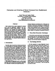
Evaluation of Dynamic Access Ordering Hardware S.A. McKee, C.W. Oliver, Wm.A. Wulf, K.L. Wright, J.H. Aylor Computer Science Report No. CS-95-46 October 30, 1995
This work was supported in part by a grant from Intel Supercomputer Division and by NSF grants MIP-9114110 and MIP-9307626.
Evaluation of Dynamic Access Ordering Hardware Sally A. McKee, Christopher W. Oliver, Wm.A. Wulf, Kenneth L. Wright, James H. Aylor Department of Computer Science Department of Electrical Engineering University of Virginia Charlottesville, VA 22903 {mckee | cwoliver | wulf | wright | jha}@virginia.edu
Abstract Memory bandwidth is rapidly becoming the limiting performance factor for many applications, particularly for streaming computations — such as scientific vector processing or multimedia (de)compression — that lack the locality of reference that makes caching effective. We describe and evaluate a system that addresses the memory bandwidth problem for this class of computations by dynamically reordering stream accesses to exploit memory system architecture and device features. The technique is practical to implement, using existing compiler technology and requiring only a modest amount of special-purpose hardware. With our prototype system, we have observed performance improvements by over 200% over normal caching.
Evaluation of Dynamic Access Ordering Hardware
Evaluation of Dynamic Access Ordering Hardware Sally A. McKee, Christopher W. Oliver, Wm.A. Wulf, Kenneth L. Wright, James H. Aylor 1. Introduction As has become painfully obvious, processor speeds are increasing much faster than memory speeds. To illustrate the current problem, consider the multiprocessor Cray T3D [Cra95]. The peak Dynamic Random Access Memory (DRAM) read bandwidth for each 150MHz DEC Alpha processor [DEC92] of this machine is 320 Mbytes/sec, or about one 64-bit word per four clock cycles. Unfortunately, the actual bandwidth may be as low as 28 Mbytes/sec — in other words, the processors can perform up to 42 instructions in the time it takes to read a single DRAM location. As Jeff Brooks explains, “the rates you see in [a T3D] application depend highly on how the memory is referenced” [Bro95]. This variance in performance occurs because the T3D’s DRAMs can perform some access sequences faster than others. Even though the term “DRAM” was coined to indicate that accesses to any “random” location require about the same amount of time, most modern DRAMs provide special capabilities that result in non-uniform access times. For instance, nearly all current DRAMs (including the T3D’s) implement a form of fast-page mode operation [Qui91,IEE92]. The sense amplifiers in fast-page mode devices behave much like a single line, or page, of cache on chip. A memory access falling outside the current page causes a new one to be loaded, making such page misses take three to five times as long as page hits. On a Cray T3D system with 16Mbit DRAMs, for instance, each page is 2048 Kbytes, page hits take about 4 cycles (26 ns), and the additional overhead for page misses takes about 15 cycles more (for about 125 ns in all) [Pal95,Bro95]. Although the terminology is similar, DRAM pages should not be confused with virtual memory pages.
1
Evaluation of Dynamic Access Ordering Hardware
With an advertised bandwidth of 500 Mbyte/s, Rambus is another interesting new memory technology [IEE92]. These bus-based systems are capable of delivering a byte of data every 2 ns for a block of information up to 256 bytes long. Like page-mode DRAMs, Rambus devices use banks of sense amplifier latches to “cache” data on chip. Unfortunately, these devices offer no performance benefit for random access patterns: the latency for accesses that miss the cache lines is 150-200 ns. The order of requests strongly affects the performance of other common devices that offer speed-optimizing features (nibble-mode, static column mode, or a small amount of SRAM cache on chip) or exhibit novel organizations (Ramlink and the new synchronous DRAM designs) [IEE92]. For interleaved memory systems, the order of requests is important on another level, as well: accesses to different banks can be performed in parallel, and thus happen faster than successive accesses to the same bank. In general, memory system performance falls significantly short of the maximum whenever accesses are not issued in an appropriate order. What is needed is a method to reorder the accesses from the natural order (that in which the processor requests them) to the optimal order for the memory system. Caches can help bridge the processor-memory performance gap for parts of programs that exhibit high locality of reference, but many computations do not reuse data soon enough to derive much benefit from caching. Codes that linearly traverse long streams of vector-like data are particularly bandwidth-limited. Unfortunately, this comprises a large and important class of computations, including scientific vector processing, digital signal processing, multi-media (de)compression, text searching, and some graphics applications, to name a few. We describe a system that addresses the memory bandwidth problem for such streaming computations by dynamically reordering stream accesses to exploit memory system architecture and device features. The technique is practical to implement,
2
Evaluation of Dynamic Access Ordering Hardware
using existing compiler technology and requiring only a modest amount of special-purpose hardware. We built a “proof of concept” dynamic access ordering system composed of a 40MHz i860 host processor and a daughterboard containing a 132-pin ASIC (of about 71,000 transistors) and associated DRAM memory. In this paper, we describe and evaluate our implementation of this hardware. Even though this is a reduced-functionality prototype system, we have observed performance improvements by over 200% over normal caching. 2. The Stream Memory Controller We describe our approach based on the simplified architecture of Figure 1. In this system, the compiler must detect the presence of streams (as in [Ben91]) and arrange to transmit information about them (i.e., base address, stride, length, data size, and whether the stream is being read or written) to the hardware at run-time. The dynamic access ordering hardware then prefetches the read operands, buffers the write operands, and reorders the accesses to get better memory system performance.
Stream Buffer Unit CPU
aesses issued in the “natural” order
CACHE
Memory Scheduling Unit
SMC
main memory
accesses issued in the “optimal” order
Figure 1 SMC Organization
Our dynamic access ordering hardware, called a Stream Memory Controller (SMC), is logically divided into two components: a Stream Buffer Unit (SBU), and a Memory
3
Evaluation of Dynamic Access Ordering Hardware
Scheduling Unit (MSU). The MSU is a controller through which memory is interfaced to the CPU. It includes logic to issue memory requests and to determine the order of requests during streaming computations. For non-stream accesses, the MSU provides the same functionality and performance as a traditional memory controller. As with the streamspecific parts of the MSU, the SBU is not on the critical path to memory, and the speed of non-stream accesses is not adversely affected by its presence. The MSU has full knowledge of all streams currently needed by the CPU: using the base address, stride, and vector length, it can generate the addresses of all elements in a stream. It also knows the details of the memory architecture, such as interleaving and device characteristics. The access-ordering circuitry uses this information to issue requests for individual stream elements in an order that attempts to maximize memory system performance.
/* tridiagonal elimination: */ for (i = 1; i < n; i++) x[i] = z[i] * (y[i] - x[i-1]);
/* SMC version: */ streamin(y+1, size, stride, n-1, FIFO0); streamin(z+1, size, stride, n-1, FIFO1); streamout(x+1,size, stride, n-1, FIFO2); reg = x[0]; for (i = 1; i < n; i++) { reg = *FIFO1 * (*FIFO0 - reg); *FIFO2 = reg; }
/* xmit stream params */
/* load x[0] */
Figure 2 SMC Programming Model
The Stream Buffer Unit contains high-speed buffers for stream operands and provides memory-mapped control registers that the processor uses to specify stream parameters. From the processor’s perspective, the stream buffers are logically implemented as a set of FIFOs within the SBU, with each stream assigned to one FIFO. The MSU accesses these
4
Evaluation of Dynamic Access Ordering Hardware
buffers as if they were random-access register files, asynchronously filling them from or draining them to memory. The processor references the next element of a stream via the memory-mapped register representing the corresponding FIFO head. By memory mapping the control registers and FIFO heads, we avoid having to modify the processor’s instruction set. Figure 2 illustrates the SMC programming model for tridiagonal elimination, one of the Livermore Loops [McM86]. 3. Experimental Implementation In order to demonstrate the viability of dynamic access ordering, we have developed an experimental Stream Memory Controller system. This proof-of-concept version is implemented as a single, semi-custom VLSI integrated circuit interfaced to an Intel i860 host processor [Int91]. The SMC ASIC was designed using VHDL for state machine specification, Mentor Graphics Corporation’s Design Architect for schematic capture, and Cascade Design Automation’s Epoch tool for hardware synthesis [Cas93,Men93]. The i860 was selected because it is both readily available and it provides the non-caching loads required for processor accesses to the SBU. Figure 3 depicts the architecture of our prototype dynamic access ordering system, which consists of the i860 node and an SMC daughtercard that connects to the motherboard via an expansion connector. The motherboard contains an i860XP processor, a system boot EPROM, a memory controller that is optimized for cache-line fills, and 16 MBytes of page mode DRAM. The daughtercard contains the SMC and its memory subsystem, along with a pipeline stage needed to meet timing and line-length constraints.
5
Evaluation of Dynamic Access Ordering Hardware
i860 Motherboard
CacheOptimized Memory Controller
40MHz i860 CPU
64 MBytes DRAM 64 MBytes DRAM
64
SMC Daughtercard
1st Pipeline Stage Discrete Components
Control 16
SMC slice 1
16
SMC slice 2
16
SMC slice 3
16
SMC slice 4
64 MBytes DRAM 64 MBytes DRAM
Figure 3 SMC System Architecture
3.1 Test Board Each bank of DRAM memory on the daughtercard is composed of two 32 MByte 60 ns page-mode components with 1 Kbyte pages. The minimum cycle time for fast page-mode accesses is 35 ns, and random accesses require 110 ns. Wait states make the SMC’s observed access time for sustained accesses 50 ns (2 CPU cycles) for page hits and 175 ns for page misses (7 CPU cycles — this includes the time to precharge and set up the new DRAM page). Since there are two interleaved banks of memory, the SMC can deliver one data item every 25 ns processor cycle for streams with relatively prime strides. The processor takes approximately 14 ns to assert its address and cycle definition pins, and the signals take another 5 ns to propagate to the expansion connector. This leaves less than 6 ns in the current cycle to latch data into or present data from the SMC. In addition, the
6
Evaluation of Dynamic Access Ordering Hardware
electrical specifications for expansion card connections call for signal line lengths of less than 1 inch before the first level of logic on the daughtercard. In light of these two constraints, we added a single-stage, bidirectional pipeline to the daughter board; this component latches the address, data, and cycle definition signals from the i860 and presents them to the SMC on the next clock cycle, or latches data from the SMC for use by the processor on the next cycle. Our off-chip implementation thus incurs pipeline delays in addition to bus turnaround delays when switching between reading and writing — delays that would not be present in an on-chip SMC. Nonetheless, the performance of our prototype SMC represents a significant improvement over the performance of a non-SMC system for stream accesses. 3.2 VLSI Chip Our prototype Stream Memory Controller is a 132-pin ASIC implemented in a 0.75 µm, three-level metal HP26B process fabricated through MOSIS. The 40MHz i860 host processor can initiate a new bus transaction every other clock cycle, and quadword instructions allow the i860 to read 128 bits of data in two consecutive clock cycles. The SMC can thus deliver a 64-bit doubleword of data every cycle. As illustrated in Figure 3, the SMC is implemented as a 4-way bit-sliced system. We chose this organization over a full 64-bit wide version because the latter would have been severely pad-limited in size. Figure 4 illustrates the decomposition of each 16-bit SMC ASIC into four logical components: the Processor Bus Interface (PBI), the Command Status and Control (CSC) registers, the FIFO Buffers, and the Bank Controller (BC).
7
Evaluation of Dynamic Access Ordering Hardware
CSC REGISTERS CSC Register Control Machine CSC DP SRAM 2-way Interleaved to i860
Memory Scheduling Unit
Processor Bus Interface (PBI)
Memory Controller FIFO Control Machine
to mem
Stream Machine
FIFO DP SRAM FIFO BUFFERS
BANK CONTROLLER
Figure 4 SMC ASIC Architecture
The PBI state machine shown at the left of Figure 4 provides the logic necessary to interface the SMC with the i860 processor bus. The PBI manages accesses to the CSC registers, stream accesses to the memory mapped FIFO heads, and non-stream (scalar) accesses to the memory subsystem. The CPU transmits the base, length, and stride parameters for each stream by writing the CSC registers. These registers are implemented with dual-ported SRAM, allowing both the CPU and the BC to access them simultaneously. The FIFO component buffers data between the processor bus and the memory system bus, and can be accessed by both simultaneously. This component is broken down into two sections: the dual-ported SRAM buffers used to implement virtual FIFOs, and the FIFO controller state machine (labeled “Stream Machine” in Figure 4), which generates the addresses for all accesses to the FIFO buffers. The FIFO controller logic provides signals conveying “fullness” information for each FIFO to both the BC and the PBI. The PBI uses these signals to determine when a given access can be completed, and the BC uses them in
8
Evaluation of Dynamic Access Ordering Hardware
its decision of which FIFO to service next. The BC logic handles the interface to the interleaved memory system and fills or drains the FIFOs as required. The BC also provides support for scalar accesses to the SMC memory space.
Figure 5 SMC ASIC Layout
The current version of the SMC, pictured in Figure 5, is 36 square millimeters and about 71,000 transistors. It includes four FIFOs that are 16 doublewords deep and can each be set to read or write. Future versions will implement adjustable-depth FIFOs that are softwareprogrammable. The prototype SMC’s Memory Scheduling Unit implements a very simple ordering policy: the BC considers each FIFO in round-robin order, performing as many accesses as it can for the current FIFO before moving on to the next. The decision of which FIFO to service next is made concurrently with the memory accesses for the current FIFO.
9
Evaluation of Dynamic Access Ordering Hardware
Despite its simplicity, this ordering strategy works well in practice; for uniprocessor systems, its performance is competitive with that of more sophisticated policies. More intelligent schemes are required to achieve good performance on computations involving streams with strides that do not hit all memory banks, and on multiprocessor systems in general [McK95b]. Further details of the design, implementation, and testing of the SMC ASIC and daughter board can be found elsewhere [McG94,Lan95]. 4. Performance Figure 6 lists the benchmark kernels used to generate the results presented here. Daxpy, copy, and scale are from the BLAS (Basic Linear Algebra Subroutines) [Don90], and tridiag is tridiagonal gaussian elimination, the fifth Livermore Loop [McM86]. Vaxpy denotes a “vector axpy” operation that occurs in matrix-vector multiplication by diagonals: a vector a times a vector x plus a vector y. For our purposes, the actual computation in these loops is unimportant. We focus instead on the access pattern, and these benchmarks are representative of the access patterns found in real codes. For instance, copy and scale are the memory access patterns of JPEG and MPEG operations in multimedia applications.
kernel
operation
types of streams
copy
for (i = 0; i < N; i++) y[i] = x[i];
1 read 1 write
daxpy
for (i = 0; i < N; i++) y[i] = a * x[i] + y[i];
1 read 1 read-modify-write
scale
for (i = 0; i < N; i++) x[i] = a * x[i];
1 read-modify-write
tridiag
for (i = 1; i < N; i++) x[i] = z[i] * (y[i] - x[i-1]);
2 read 1 write
vaxpy
for (i = 0; i < N; i++) y[i] = a[i] * x[i] + y[i];
2 read 1 read-modify-write
Figure 6 Benchmark Algorithms
10
Evaluation of Dynamic Access Ordering Hardware
We present our results both as a percentage of peak bandwidth — i.e., that which would be achieved if the CPU could perform one memory access each processor cycle — and as the average number of cycles per access. The vectors we consider here are of equal length, unit stride, share no DRAM pages in common, and are aligned to begin in the same bank. In order to put as much stress as possible on the memory system, arithmetic computation is assumed to be infinitely fast, and is abstracted out of each kernel. We execute each loop prior to beginning our measurements so that the experiment can run entirely out of the instruction cache. All stream references use non-caching loads and stores. Figure 7 illustrates the measured performance of our prototype system on each of the benchmark kernels on vectors of 16 to 8192 elements. The graphs on the left show the percentage of the peak system bandwidth exploited for each benchmark. Those on the right present the same information in a complementary format that helps put the bandwidth percentages into perspective for this particular machine: the average number of processor cycles per stream access. The dashed lines labeled “attainable bandwidth” indicate performance limits due to SMC startup costs, unavoidable page misses, or the cost of moving data between the SMC and CPU chips (see [McK95b] for derivations of performance bounds), and the solid lines indicate the performance of our access ordering hardware. The dotted lines indicate the performance measured when using “normal” caching load instructions to access the stream data in the i860’s own cache-optimized memory; and the dot-dash lines indicate the performance measured when using the i860’s non-caching pipelined floating point load (pfld) instruction.
11
Evaluation of Dynamic Access Ordering Hardware
Percent of Peak Bandwidth
Average Cycles/Access
performance limit hardware SMC performance hardware cache performance hardware pfld performance
60 40 20
cycles / access
5
80
bandwidth
copy
100
3 2 1
(a)
vector length
16 32 64 128 256 512 1K 2K 4K 8K
0 16 32 64 128 256 512 1K 2K 4K 8K
0
4
(b) cycles / access
5
80
bandwidth
daxpy
100
60 40 20
4 3 2 1
vector length
16 32 64 128 256 512 1K 2K 4K 8K
0 16 32 64 128 256 512 1K 2K 4K 8K
0
(c)
(d) cycles / access
60 40 20
4 3 2 1
vector length
16 32 64 128 256 512 1K 2K 4K 8K
0 16 32 64 128 256 512 1K 2K 4K 8K
0
(f)
vector length
cycles / access
5
80
bandwidth
scale
100
60 40 20
4 3 2 1
vector length
16 32 64 128 256 512 1K 2K 4K 8K
0 16 32 64 128 256 512 1K 2K 4K 8K
0
(g)
(h)
vector length
5
cycles / access
bandwidth
80 60 40 20
4 3 2 1 0
vector length
16 32 64 128 256 512 1K 2K 4K 8K
0 16 32 64 128 256 512 1K 2K 4K 8K
vaxpy
100
(i)
vector length
5
80
bandwidth
tridiag
100
(e)
vector length
(j)
vector length
Figure 7 Comparative Performance
12
Evaluation of Dynamic Access Ordering Hardware
Performing the computation in the natural order with caching accesses yields less than 32% of the system’s peak bandwidth for all access patterns. The effective bandwidth delivered by the SMC for these kernels is between 202% and 305% of that delivered by normal caching. Looking at it from a different perspective, the SMC brings the average cycles per memory access very close to the minimum one cycle for long-vector computations. In contrast, the average number of cycles per access when using the cache is more than three. The disparity between SMC and cache performance would be even more dramatic for nonunit stride computations, since in this case each cache-line fill would fetch unneeded data. For instance, at a stride of five, the SMC could deliver 12 times the effective bandwidth of the cache (for an average of one cycle for each element accessed via the SMC, versus over 12 cycles for each one accessed through the cache). When non-caching instructions are used (e.g., if the programmer does not want stream data to entirely fill the cache), performance is generally even worse than when using caching loads. The exception to this is the scale benchmark, results for which are shown in Figure 7(g) and (e). This kernel operates on a single vector, thus it accesses every element in a single DRAM page before switching to a different page. In contrast, each cache-line fill incurs a DRAM page miss for the first word in the line, regardless of whether or not it is on the same DRAM page as the previously loaded cache line. Performance of the benchmarks using the pfld instruction could take more advantage of fast-page mode — and thus improve performance — by unrolling the loops and grouping accesses to each stream, so that several accesses that hit the current page are issued after every DRAM page miss (see Section 5 for more details). The patterns of the performance curves in graphs for different benchmarks are almost boringly similar. Our results indicate that variations in the processor’s reference sequence have little effect on the SMC’s ability to improve bandwidth. The slight dips in the SMC performance curves at 32-element vectors for the tridiag and vaxpy kernels occur because
13
Evaluation of Dynamic Access Ordering Hardware
of an interaction between the number of streams, the vector length, and the FIFO depth. Exactly when the DRAM page misses happen depends on all these parameters, and the shorter the vectors are, the greater the impact each page miss has on overall performance: amortizing the last page miss over just a few more accesses can make a noticeable difference. The result is that when we plot points for vectors of every length, we see a sawtooth shape, the “teeth” of which get smaller as vector length grows, i.e., as DRAM page misses are amortized over more total accesses. Figure 8 shows this detail in the bus-level simulation performance for the copy benchmark.
100
% peak bandwidth
80
60 functional simulation hardware performance 40
20
1K
512
256
128
64
32
16
0
vector length
Figure 8 copy Detail of SMC Performance as Vector Length Grows
Even an SMC with only a small amount of buffer space can consistently deliver over 80% of the peak system bandwidth. When we take each kernel’s inherent bandwidth limits into account, these SMC performances represent between 89% and 98% of the attainable bandwidth for vectors over 128 elements. Our simulation studies indicate that SMCs with deeper FIFOs can exploit nearly the full system bandwidth for long-vector computations [McK95b].
14
Evaluation of Dynamic Access Ordering Hardware
5. Related Work The notion that performance of memory-intensive applications can be improved by reordering memory requests has been demonstrated before. Unique to our work is the premise that, for stream-like reference patterns, access ordering: -
should be performed to exploit both memory system architecture and device component capabilities, and
-
should be done at run-time, when more information is available on which to base scheduling decisions.
Our confidence that the SMC could be implemented efficiently was based on the fact that similar designs have been built. For instance, the organization of the SBU is almost identical to the stream units of the WM architecture [Wul92], and the SMC may be thought of as a special case of a decoupled access-execute architecture [Goo85,Smi87]. More complex stream buffers have been evaluated in other contexts. Jouppi performed simulation studies of stream buffers used to prefetch successive cache lines on a cache miss [Jou90], and Palacharla and Kessler investigate the use of a set of stream buffers as a replacement for secondary cache [Pal94]. Although the latter scheme generally increased the cache hit rates of the benchmarks they simulated, these improvements were achieved at the expense of increased main memory bandwidth requirements. In contrast, our approach attempts to exploit the existing memory bandwidth as much as possible, without increasing bandwidth requirements. It is often possible to take advantage of memory component features by reordering memory accesses at compile time. For instance, the compiler optimizations of Alexander, et al., for wide-bus machines [Ale93] have the side-effect of exploiting DRAM features like fastpage mode. Moyer unrolls loops and groups accesses to each stream, so that the cost of each DRAM page-miss can be amortized over several references to the same page [Moy93]. Lee’s subroutines to mimic Cray instructions on the Intel i860XR include another purely
15
Evaluation of Dynamic Access Ordering Hardware
compile-time approach: he treats the cache as a pseudo “vector register” by reading vector elements in blocks (using non-caching load instructions) and then writing them to a preallocated portion of cache [Lee93]. Meadows describes a similar scheme for the PGI i860 compiler [Mea92], and Loshin and Budge give a general description of the technique [Los92]. A subset of these authors measured the time to load a single vector via Moyer’s and Lee’s schemes on a node of an iPSC/860, observing performance improvements between about 40% to 450% over normal caching, depending on the stride of the vector [McK95a]. Another option is to augment the purely compile-time approach with a hardware assist. Palacharla and Kessler [Pal95] investigate code restructuring techniques to exploit fastpage mode DRAMs via a hardware read-ahead mechanism on the Cray T3D. On a cache miss, the memory controller first performs the cache-line fill, then the read-ahead hardware automatically prefetches the next consecutive cache line and stores it in a stream buffer inside the memory controller. If the next cache miss hits in the stream buffer, the entire line is transferred to cache, and the next cache line of data is prefetched. If the next cache miss misses in the stream buffer, the buffer’s contents are discarded, the desired line is fetched for the cache, and the subsequent line is prefetched. Palacharla and Kessler measure a performance improvement of up to 75% in two, three, and four-stream examples on a Cray T3D [Pal95], and Brooks demonstrates a factor of 13 improvement (from 3.5 Mflops to 51.6 Mflops) in T3D performance after applying access ordering to a 3x3 matrix multiplication routine used in Quantum Chromo Dynamics (QCD) codes [Bro94]. The benefits of compile-time ordering schemes can be substantial, but their performance cannot rival that of a hardware scheme such as the one discussed here. The compiler cannot generate the optimal access sequence without the address alignment information that is usually only available at run time. For this reason, Palacharla and Kessler generate code to decide at run-time the extent to which their optimizations should be applied. And for
16
Evaluation of Dynamic Access Ordering Hardware
systems with fast-page mode DRAMs, the compiler cannot determine where stream data crosses DRAM page boundaries. Even bigger limitations are that any scheme using the cache to load stream data suffers from cache conflicts, and any scheme loading the data directly to registers suffers from register pressure. 6. Lessons Learned Some of the results of our studies verified our expectations, while others initially surprised us. For instance, we proved (as expected) that the SMC can be fabricated with synthesis to meet its timing requirements and that it performs as expected: the SMC delivers over 90% of the attainable bandwidth for long-vector computations, even though it resides on a separate chip from the CPU. We verified that the SMC yields two to three times the effective bandwidth delivered by the i860’s own (cache-optimized) memory system. In addition, we reaped the benefits of a multifaceted approach to modeling and simulating our design before committing it to silicon. We employed five different models (two analytic models, one functional simulator, one gate-level hardware simulator, and one petri-net based system model) designed for different purposes by three different teams of people in two different academic departments [McK95c]. The common starting point was a description of the hardware interface and high-level (functional) behavior. These models helped us to refine and validate each stage of our design, but several of their results were unexpected. First, FIFO depth must be tailored to the parameters of a particular computation. Long-vector computations benefit from very deep FIFOs, whereas computations on shorter streams require shallower FIFOs. We have derived algorithms that compilers can use to calculate an appropriate FIFO depth for a particular computation on a given system [McK95b]. The need for adjustable FIFO depth comes from the start-up cost associated with using the SMC. At the beginning of a computation reading s streams, the processor will stall waiting
17
Evaluation of Dynamic Access Ordering Hardware
for the first element of stream s while the MSU fills the FIFOs for the first s – 1 streams. By the time the MSU has provided all the operands for the first loop iteration, it will also have prefetched enough data for many future iterations, and the computation can proceed without stalling the processor again soon. This means that deeper FIFOs cause the processor to wait longer at startup. On the other hand, deep FIFOs allow the SMC to amortize page-miss costs more effectively. Figure 9 shows the net effect of these competing performance factors for vaxpy on vectors of length 100 and 10,000. If the vectors in the computation are sufficiently long, as in Figure 9(b), the initial delay becomes insignificant. Short vectors afford fewer accesses over which to amortize startup and page-miss costs, and thus for the vectors of Figure 9(a), initial delays
100 80 attainable bandwidth functional simulation hardware simulation
60 40 20
% peak bandwidth
100
60 40 20
(a)
FIFO depth
(b)
512
256
64
128
32
8
512
256
64
128
32
8
0 16
0
80
16
% peak bandwidth
represent a significant portion of the computation time.
FIFO depth
Figure 9 vaxpy SMC Performance as FIFO Depth Grows
We were also surprised to discover that, in many cases (particularly for uniprocessor SMC systems), a relatively naive access-ordering policy performs competitively with a more sophisticated heuristic. Furthermore, the programmer or compiler can often arrange to avoid the situations in which a simple policy would perform poorly. Finally, we did not expect the need to pipeline the hardware so much in order to meet timing requirements.
18
Evaluation of Dynamic Access Ordering Hardware
7. Conclusions By combining compile-time detection of streams with execution-time selection of the access order and issue, we achieve near-optimal bandwidth for vector-like accesses relatively inexpensively. This technique complements more traditional cache-based schemes, so that overall effective memory performance need not be a bottleneck. The dynamic access ordering hardware described here is both feasible and efficient to implement. The SMC neither increases the processor’s cycle time nor lengthens the path to memory for non-stream accesses. The hardware complexity is a function of the number and size of the stream buffers (implemented as FIFOs) and SMC placement (whether or not it is integrated into the processor chip). Using commercially available memory parts and only a few hundred words of buffer storage, our proof-of-concept system demonstrates that an SMC system can deliver nearly the full memory system bandwidth. Moreover, it does so without heroic compiler technology. The current version uses about 71,000 transistors and features four moderate-size FIFOs; this is a relatively modest number of transistors when compared to the 3-10 million used in current microprocessors. SMC complexity is expected to scale linearly with increasing FIFO depth. This prototype version places the SMC on a separate board from the processor, but for best performance, we believe the dynamic access ordering hardware should be integrated onto the processor chip, at the same level as an L1 cache. The next stage of the project targets building an SMC system in which the stream buffers reside on-chip with a high-speed microprocessor. We have implemented dynamic access ordering within the context of memory systems composed of fast page-mode DRAMs, but the technique may be applied to other memory systems, as well. In addition to taking advantage of memory component features (for those devices that have non-uniform access times), prefetching read operands, and buffering
19
Evaluation of Dynamic Access Ordering Hardware
writes, the SMC provides the same functionality as the conflict-avoidance hardware used in many vector computers (in fact, the SMC is more general, delivering good performance under a wider variety of circumstances). Furthermore, the SMC can achieve vector-like memory performance for streamed computations whose data recurrences prevent vectorization. Preliminary investigations indicate that the SMC concept can be effectively applied to shared-memory multiprocessor systems, but that a sophisticated ordering strategy is required for such systems to achieve uniformly high performance. Long-range plans involve building an experimental multiprocessor SMC system to validate these findings.
20
Evaluation of Dynamic Access Ordering Hardware
References [Ale93]
M.J. Alexander, M.W. Bailey, B.R. Childers, J.W. Davidson, and S. Jinturkar, “Memory Bandwidth Optimizations for Wide-Bus Machines”, Proc. 26th Hawaii International Conference on Systems Sciences (HICSS-26), January 1993, pages 466-475. (incorrectly published under M.A. Alexander, et al.)
[Ben91]
M.E. Benitez and J. W. Davidson, “Code Generation for Streaming: An Access/ Execute Mechanism”, Proc. Fourth International Conference on Architectural Support for Programming Languages and Operating Systems (ASPLOS-IV), April 1991, pages 132-141.
[Bro95]
J. Brooks, “Single PE Optimization Techniques for the Cray T3D System”, Proc. 1st European T3D Workshop, September, 1995.
[Cas93]
Epoch User’s Manual 3.1, Cascade Design Automation, 1993.
[Cra95]
“Cray T3D Massively Parallel Processing System”, Cray Research, Inc., http:// www.cray.com/PUBLIC/product-info/mpp/CRAY_T3D.html, 1995.
[Dec92]
Digital Technical Journal, Digital Equipment Corporation, 4(4), Special Issue, 1992, http://www.digital.com/info/DTJ/axp-toc.html.
[Don90]
J. Dongarra, J. DuCroz, I. Duff, and S. Hammerling, “A set of Level 3 Basic Linear Algebra Subprograms”, ACM Transactions on Mathematical Software, 16(1):1-17, March 1990.
[Goo85]
J.R. Goodman, J. Hsieh, K. Liou, A.R. Pleszkun, P.B. Schechter, and H.C. Young, “PIPE: A VLSI Decoupled Architecture”, Proc. 12th International Symposium n Computer Architecture (ISCA), June 1985, pages 20-27.
[IEE92]
“Memory Catches Up”, Special Report, IEEE Spectrum, 29(10):34-53 October 1992.
[Int91]
i860 XP Microprocessor Data Book, Intel Corporation, 1991.
[Jou90]
N.P. Jouppi, “Improving Direct-Mapped Cache Performance by the Addition of a Small Fully-Associative Cache and Prefetch Buffers. Proc. 17th International Symposium on Computer Architecture (ISCA), May 1990, pages 364-373. Also Digital Equipment Corporation, Western Research Lab, Technical Note TN-14, March 1990.
[Lan95]
T.C. Landon, R.H. Klenke, J.H. Aylor, M.H. Salinas, and S.A. McKee, “An Approach for Optimizing Synthesized High-Speed ASICs”, Proc. of the IEEE International ASIC Conference (ASIC’95), Austin, TX, September 1995, pages 245-248.
21
Evaluation of Dynamic Access Ordering Hardware
[Lee93]
K. Lee, “The NAS860 Library User’s Manual”, NAS Technical Report RND93-003, NASA Ames Research Center, Moffett Field, CA, March 1993.
[Los92]
D. Loshin, and D. Budge, “Breaking the Memory Bottleneck, Parts 1 & 2”, Supercomputing Review, Jan./Feb. 1992.
[McG94] S.W. McGee, R.H. Klenke, J.H. Aylor, and A.J. Schwab, “Design of a Processor Bus Interface ASIC for the Stream Memory Controller”, Proc. of the IEEE International ASIC Conference (ASIC’94), Rochester, NY, September 1994, pages 462-465. [McK95a] S.A. McKee, Wm.A. Wulf, “Access Ordering and Memory-Conscious Cache Utilization,” Proc. First International Symposium on High Performance Computer Architecture, Raleigh, NC, January 1995, pages 253-262. [McK95b] S.A. McKee, “Maximizing Memory Bandwidth for Streamed Computations”, Ph.D. Dissertation, University of Virginia, Department of Computer Science, May 1995. [McK95c] S.A. McKee, D.A.B. Weikle, K.L. Wright, C.W. Oliver, T.C. Landon, A.P. Voss, Wm.A. Wulf, J.H. Aylor, “Avoiding Irreproducible Results: Modeling the Stream Memory Controller”, University of Virginia, Department of Computer Science, Technical Report CS-95-46, Oct. 1995. [McM86] F.H. McMahon, “The Livermore Fortran Kernels: A Computer Test of the Numerical Performance Range”, Lawrence Livermore National Laboratory, UCRL-53745, December 1986. [Mea92]
L. Meadows, S. Nakamoto, and V. Schuster, “A Vectorizing Software Pipelining Compiler for LIW and Superscalar Architectures”, Proc. RISC’92, pages 331-343.
[Men93]
System-1076, Quicksim II User’s Manual, Mentor Graphics Corporation, 1993.
[Moy93] S.A. Moyer, “Access Ordering and Effective Memory Bandwidth”, Ph.D. Dissertation, University of Virginia, Department of Computer Science Technical Report CS-93-18, April 1993. [Pal94]
S. Palacharla and R.E. Kessler, “Evaluating Stream Buffers as a Secondary Cache Replacement”, Proc. 21st International Symposium on Computer Architecture (ISCA), May 1994, pages 24-33.
[Pal95]
S. Palacharla and R.E. Kessler, “Code Restructuring to Exploit Page Mode and Read-Ahead Features of the Cray T3D”, Cray Research Internal Report, February 1995.
[Qui91]
R. Quinnell, “High-speed DRAMs”, EDN, May 23, 1991.
22
Evaluation of Dynamic Access Ordering Hardware
[Smi87]
J.E. Smith, G.E. Dermer, B.D. Vanderwarn, S.D. Klinger, C.M. Roszewski, D.L. Fowler, and D.R. Scidmore, “The ZS-1 Central Processor”, Proc. 2nd International Conference on Architectural Support for Programming Languages and Systems (ASPLOS-II), Oct. 1987, pages 199-204.
[Wul92]
Wm.A. Wulf, “Evaluation of the WM Architecture”, Proc. 19th International Symposium on Computer Architecture (ISCA), May 1992, pages 382-390.
23
Evaluation of Dynamic Access Ordering Hardware
24