AN OPEN SYSTEM-ON-CHIP PLATFORM FOR EDUCATION
DONALD W. BOULDIN and RISHI R. SRIVASTAVA Electrical & Computer Engineering University of Tennessee Knoxville, TN 37996-2100
[email protected] 1. Introduction Million-gate integrated circuits are increasingly being designed as system-onchip (SoC) platforms since platform design mitigates the risks involved with integrating a CPU core and other virtual components by a fixed deadline. Using this approach, designers can overcome uncertainties about the quality of the components and their interaction and can produce derivative designs rapidly. The development of a SoC platform is described in this paper. In the process of conducting this team project, students learned not only to reuse existing cores but also the requirements to create high quality cores for reuse. The SoC platform, which uses only open cores that can be obtained by anyone at no charge, can also serve as an “industrial strength” design for students to learn about optimizations at the logic and physical levels. Thus, students can exercise synthesis and place/route tools to explore the power-delay-area solution space of a million-gate design. Having internal visibility of the components at both the source code level and at the physical layout level greatly facilitates their understanding of SoC issues. The SoC platform is being placed in the public domain so that others may contribute to its enhancement. 2. Project Goals and Core Selection Today designers of application-integrated circuits are faced with the challenge of creating and verifying the content of million-transistor chips as quickly as possible in order to reduce the time-to-market [1]. It has been estimated that a one-month delay in bringing a product to market can result in a loss of ten percent of the potential revenue [2]. Hence, not all of the transistors on these chips can be customized but instead must be ported from previous designs. These reusable cores or intellectual property (IP) blocks include CPUs (like ARM, PowerPC and LEON), MPEG decompression engines, PCI bus controllers, specialized DSPs, etc. Combining several complex cores using standard cells is much more manageable and quicker than designing millions of transistors one at a time. The myth that characterizes today’s IP is that these components are blocks that have well-defined contents and interfaces. However, they are often fuzzy and hence appear more like patches in a quilt, which must be stitched together. The components cannot be
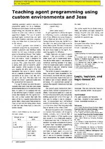
assembled blindly and rapidly, but rather must be carefully pieced together to form a working system. Therefore, design for reuse does not come free. Thus, universities and individuals can and are developing open SoCs to serve as education and research platforms [3]. In our graduate program at the University of Tennessee [4], ECE 652 involves advanced physical level design. Thus, students exercise synthesis and place/route tools to explore the powerdelay-area solution space of a million-gate design. Having internal visibility of the components at both the source code level and at the physical layout level greatly facilitates their understanding of SoC issues. In support of the goals of ECE 652, we designed and implemented a baseline SoC platform targeting the TSMC-0.18 CMOS process. To enhance the students’ understanding of SoC issues, we selected only open soft cores that could be obtained for free [5-6] or generated internally. For the CPU, we selected the LEON-2 processor [5], which is Sparc-V8 compatible. As shown in Figure 1, it provides direct memory interfaced PROM, memory mapped I/O, SRAM, SDRAM with variable memory width of 8, 16 or 32 bits. The LEON-2 processor can also include various other features such as two UARTs, interrupt controller, memory controller, and an interface for a coprocessor or floating point unit. A flexible configuration scheme makes it straightforward to add new cores as masters or slaves depending upon their functionality. The LEON-2 processor also has separate data and instruction cache RAMs which can be generated in 1-4 sets each of 1-64Kb depending on the functionality desired. The compiler for the LEON-2 is LECCS (Leon/Erc32 GNU Cross-Compiler System) which is compatible with Sun Solaris / Linux / Windows operating systems. LECCS supports ordinary sequential C/C++ programming or multitasking using RTEMS (Real Time Embedded Micro-controller Systems) kernel. 3. Platform SoC Design and Verification Flow The entire ECE 652 class of sixteen graduate students was divided into small groups working independently on cores so it was essential to define some specifications and standards to enable the integration of these into a complete SoC at a later stage. Each core was verified individually via pre-layout simulation, synthesis, place/route and post-layout simulation prior to attempting integration with the LEON-2 or other cores. Thus, we could be assured that adding a new core to our SoC design would not introduce any errors within that core and we need only test for its interaction with the rest of the SoC platform. The task of integrating these cores into a SoC platform is greatly facilitated by using a common bus protocol to interconnect them. For this purpose, an AMBA–wrapper was created for each core such that it would enable the cores to act as AHB bus masters and APB bus slaves. Although each core had a different data width and operating procedures, it was decided that the data width would be 32 bits and each core would start its work when given a proper control signal. The size of the RAMs added to individual cores was also fixed. At this point our strategy of predefining the style of communication among cores proved most advantageous, as the same wrapper could be used for other
cores with minor modifications. Different cores can access on-chip peripherals using AMBA busses and simultaneous bus requests can be handled by defining priorities for each core. A core acting as a bus master can access the bus only when granted permission by the AHB controller. However, it can perform its function once the data has been loaded into its RAM and given the go-ahead signal without the need to continue having bus control. Various design constraints and incremental synthesis techniques were used to achieve a correct simulation of the LEON-2 processor with other cores. Artisan RAMs were added to the design and, with proper power planning techniques, place and route of the design was completed. 4. Conclusions and Plans An open SoC platform, which uses only open cores that can be obtained by anyone at no charge, has been developed, implemented and verified as an “industrial strength” design for students to learn about optimizations at the logic and physical levels. The SoC platform is being placed in the public domain so that others may contribute to its enhancement. ACKNOWLEDGMENTS We gratefully acknowledge Synopsys, Mentor Graphics and Cadence Design Systems for support of the laboratory with their integrated circuit design tools. REFERENCES [1] International Technology Roadmap for Semiconductors, http://public.itrs.net/ [2] Smith, M. J. S., Application-Specific Integrated Circuits, Addison-Wesley, Boston, MA, 1997. [3] Bolado, M., Castillo, J., Posadas, H., Sanchez, P., Villar, E., Sanchez, C., Blasco, P. and H. Fouren, “Platform Based on Open-Source Cores for Industrial Applications”, Proceedings of the 2004 Design Automation and Test in Europe, Paris, France, (to appear), 16-20 Feb. 2004. [4] Bouldin, D.W, Microelectronic Systems Courses, University of Tennessee, http://vlsi1.engr.utk.edu/ece/bouldin_courses/ [5] Gaisler Research, http://www.gaisler.com/
[6] Open Cores, http://www.opencores.org/
Fig. 1. Block Diagram of the Open SoC Platform.
Fig. 2. Platform SoC Design and Verification Flow.