Microelectronic Engineering 187–188 (2018) 27–32
Contents lists available at ScienceDirect
Microelectronic Engineering journal homepage: www.elsevier.com/locate/mee
Research paper
Fabrication of microfluidic devices with 3D embedded flow-invasive microelements Bobby Mathew a, Anas Alazzam b,c,d,⁎, Saud Khashan e, Ion Stiharu c, Sawsan Dagher a, Edward P. Furlani f a
Department of Mechanical Engineering, UAE University, Abu Dhabi, Al-Ain, United Arab Emirates Department of Mechanical Engineering, Khalifa University, Abu Dhabi, United Arab Emirates Department of Mechanical and Industrial Engineering, Concordia University, Montreal, Canada d Electrical Engineering Department, École de Technologie Supérieure, Montreal, Canada e Department of Mechanical Engineering, Jordan University of Science and Technology, Irbid, Jordan f Departments of Chemical and Biological Engineering and Electrical Engineering, University at Buffalo SUNY, NY, USA b c
a r t i c l e
i n f o
Article history: Received 27 September 2017 Received in revised form 14 November 2017 Accepted 21 November 2017 Available online 23 November 2017 Keywords: Dielectrophoresis Microfabrication Magnetophoresis 3D microelements Flow invasive microelements
a b s t r a c t A process is demonstrated for fabricating microfluidic devices with pre-fabricated microelements embedded within a microchannel orthogonal to the flow. The microelements constitute a functional three-dimensional (3D) structure that can be used for a broad range of applications. The process is demonstrated using PDMS and glass and conventional microfabrication processes. The use of this process for applications of dielectrophoresis and magnetophoresis is discussed. © 2017 Elsevier B.V. All rights reserved.
1. Introduction Microfluidic devices based on dielectrophoresis and magnetophoresis are increasingly used for the detection, sorting, and analysis of microscale biomaterials including cells, bacteria, viruses, and beads/particles [1–3]. Many of these devices are fabricated using conventional top-down clean room based techniques that have been adapted from the microelectronics industry [4]. However, these methods are not well-suited for producing 3D microstructures within a microchannel to provide, for example, a desired electric field/force distribution that spans the entire height of the channel. One way to achieve this is to arrange elements within a microchannel in a stair-step fashion as shown in Fig. 1. This figure shows electric and magnetic field distributions within a microchannel due to 3D configurations of conductive and magnetic microelements, respectively. The electric and magnetic fields for a conventional planar arrangement of conductive and magnetic microelements on the base of a microchannel are shown in Fig. 1a and c. Note that the effective range of the fields is limited to a close proximity to the elements. However, the field distributions can be significantly extended if the elements are arranged in a stair-step fashion and embedded lengthwise along the width of the channel orthogonal to the flow ⁎ Corresponding author at: Department of Mechanical Engineering, Khalifa University, Abu Dhabi, United Arab Emirates. E-mail address:
[email protected] (A. Alazzam).
https://doi.org/10.1016/j.mee.2017.11.013 0167-9317/© 2017 Elsevier B.V. All rights reserved.
as shown in Fig. 1b and d. Voltages can be applied to embedded electrodes to create the desired electric field distribution throughout the height of the microchannel as shown in Fig. 1b. This 3D stair-step structure will provide enhanced dielectrophoresis over conventional electrode configurations. Similarly, Fig. 1d, shows a 3D stair-step arrangement of rectangular soft-magnetic microelements within a microchannel. When an external bias field is applied, the elements become magnetized and produce a magnetic field throughout the height of the microchannel that provides enhanced magnetophoreis [5]. The ability to fabricate such 3D structures can enable the use of deep microchannels for dielectrophoresis and magnetophoresis, which in turn enables enhanced throughput and enhanced performance. To date, researchers have integrated 3D electrodes in microfluidic devices for applications involving dielectrophoresis and magnetophoresis. Several researchers have realized 2D arrays of 3D vertical electrodes arranged inside a microchannel by electroplating gold or electroforming copper using a SU-8 mold as well as coating SU-8 pinfins with carbon [6,7]. 3D vertical metallic electrodes have also been created on the sidewalls of a microchannel by electroplating, directly on the wafer, as well as manually aligning metallic structures, including spheres and cubes, during assembly of the final microdevice [8–10]. Horizontal electrodes are usually created by curing a slurry of liquid PDMS and electrically conductive powder that is filled in perpendicular slots that open towards the fluidic channel. Silver powder and carbon nanotubes have been used as the conductive powder [11,12]. In
28
B. Mathew et al. / Microelectronic Engineering 187–188 (2018) 27–32
Fig. 1. Cross-section view of field gradients inside a microchannel due to different arrangements of microelements: a and b show the electric potential due to electrodes; c and d show the magnetic field due to soft-magnetic elements subjected to a bias field. A conventional arrangement of elements on the base of the channel shown in a and c, and stair-step arrangement of elements shown in b and d.
addition, it is also common to use planar electrodes on both the top and bottom substrates of a microfluidic device for maintaining a desired field distribution over the entire height of the microchannel [13,14]. However, while planar electrodes can be considered to form a 3D configuration, they do not create the same effect as the fully 3D electrode structure described above. With regards to magnetophoretic chips, there has been several successful attempts at realizing vertically as well as horizontally aligned magnetic elements within a microfluidic device. One such method involves electroplating a single nickel microstructure that is horizontally aligned along the direction of flow and located centrally inside the microchannel [15]. Magnetophoretic chips have been fabricated by embedding magnetic elements on both sidewalls of the microchannel in order to generate a magnetic field gradient across the width of the microchannel [16]. In another scenario, horizontally aligned magnetic elements that span the entire width of a microchannel are integrated on the bottom surface via electroplating or sputtering [17,18]. Recently, a magnetophoretic chip has been developed with vertically aligned multiple magnetic elements (composite of carbonyl-iron microparticle and PDMS) arranged in an in-line fashion and located centrally inside the microchannel [19]. Magnetophoretic chips have also been developed with sub-millimeter strips of magnetic elements placed externally on top of the microdevice such that the tip aligns with the side wall of the microchannel [20]. Below we detail a novel microfabrication process for embedding horizontal prefabricated microelements within a microfluidic device so that they span the width of a microchannel lengthwise, in a stairstep fashion as shown in Fig. 2. This process can be used to create novel functional 3D microstructures that are useful for a broad range of microfluidic applications, e.g. dielectrophoresis and magnetophoresis as described above. To our best knowledge, no microfabrication process has been reported for creating such structures.
the pre-fabricated microelements are positioned inside each slot as shown in Fig. 2b, following which the PDMS substrate is sealed with the glass plate, Fig. 2c. Next, liquid PDMS is introduced into these slots from the outside to fill the slots via capillary action. Once the slots are filled, the microdevice is baked to cure the PDMS in the slots, which yield the final device structure of Fig. 2d. Standard microfabrication processes such as multi-layer photolithography, casting, and bonding are used for building the microdevice. The casting PDMS mold is created by carrying out multi-layer photolithography on a silicon wafer which functions as the substrate. The microfabrication process layout for realizing the mold is depicted in schematic form in Fig. 3. SU-8, specifically SU-8 2075, is used as the photoresist. With this particular photoresist it is possible to build layers with thickness close to the diameter of the microelements, which in this case is 127 μm. Multi-layer photolithography is used to build this microdevice since the microelements are to be positioned at different heights. The process starts with spin coating (WS650HZB-23NPP/UD3/ UD3B/OND from Laurell Technologies Corporation) the first SU-8 layer on the silicon wafer, as illustrated in Fig. 3a and b. This is followed by further processing of the first layer including a pre-exposure bake (Cimarec Digital Hotplate from Thermo Scientific), UV exposure (Dilase 650 from KLOE, Montpellier, France) and post-exposure bake. The front view of the process layout is shown on the left side of Fig. 3 while that on the right side is the top view. The recipe used for each step associated
2. Methods The envisioned microfluidic device, with embedded 3D prefabricated microelements, is shown in Fig. 2. The structure is made up of two layers, PDMS and glass. The microchannel including the microelements and manifolds are contained in the PDMS layer while the glass substrate functions as the lid. The microdevice contains three metallic microelements that are horizontally embedded lengthwise in a stair-step fashion, orthogonal to the flow in the microchannel. The proposed approach to fabricating this device is depicted in Fig. 2. In the first step of the process shown in Fig. 2a, a PDMS substrate is created with slots of varying depths but with the same planar dimensions. The width of each slot is the same as the width of the microelement. Next,
Fig. 2. Schematic of the proposed microdevice and microfabrication process.
B. Mathew et al. / Microelectronic Engineering 187–188 (2018) 27–32
29
Fig. 3. Schematic of process layout of microfabrication of SU-8 mold.
with photolithography is the same as that provided in the datasheet of SU-8 [21]. It can be noticed from Fig. 3c that during the first UV exposure step, only the regions of the SU-8 layer corresponding to the first slot in
the PDMS are exposed. After the post-exposure bake, and prior to development, the second layer of SU-8 is spin coated on top of the first layer of SU-8, Fig. 3d, using the same spin-speed as that used for the first layer.
30
B. Mathew et al. / Microelectronic Engineering 187–188 (2018) 27–32
Afterwards the entire SU-8 layer is subjected to pre-exposure bake, UV exposure, and post-exposure bake, Fig. 3e. The bake time used at this stage is same as that corresponding to the thickness of the second layer rather than the thickness of the entire SU8 layer. During UV exposure, the regions of the SU-8 layer corresponding to second slot in the PDMS layer are exposed as illustrated in Fig. 3e. The dose for this UV exposure step corresponds to that of the entire thickness of the SU-8. Following the second post-exposure bake, a third layer of SU-8 is spun onto the SU-8 layer on top of the silicon wafer, Fig. 3f. Subsequently, the entire SU-8 layer is subjected to a preexposure bake, UV exposure, removal and post-exposure bake. The duration of pre- and post-exposure bakes are maintained the same as that corresponding to the thickness of the third layer; however, the UV exposure dose corresponding to the thickness of the entire SU-8 layer is used. During the exposure step, the SU-8 layers that corresponds to the third slot and microchannel in the PDMS are exposed, Fig. 3g and h. As this is the last layer, development is carried out after completion of the post-exposure bake. Upon completion of the development step,
all the unexposed SU-8 regions are removed leaving behind the pattern shown in Fig. 3i. From this figure it can be noticed that there are additional rectangular microstructures at the end of the SU-8 corresponding to slots in PDMS. The height of these additional SU-8 microstructures is same as the height of the SU-8 microstructure corresponding to the microchannel in PDMS. The purpose of these SU-8 microstructures is to realize small vertical holes in the PDMS layer through which the liquid PDMS would be introduced into the slots after placing the microelements for sealing of the microchannel. Fig. 4a and b are two photographs of the front view of the microstructures, corresponding to slots in PDMS, as obtained using Scanning electron microscope and an optical microscope, respectively. It can be noticed from these two figures that layers are seamless. Also, the images provide an indication of the height of each of the SU-8 structures. The width of the microstructures that corresponds to the slots in PDMS is 150 μm while that of the microstructure corresponding to the microchannel in PDMS is 300 μm. Fig. 4c shows the 3D profile of the SU8 microstructure as obtained using a profilometer. The height of microstructures that corresponds to the
Fig. 4. Images of SU-8 microstructures on silicon; (a) SEM image, (b) front view as observed through an optical microscope and (c) perspective view, of a section, obtained from profilometer indicating height.
B. Mathew et al. / Microelectronic Engineering 187–188 (2018) 27–32
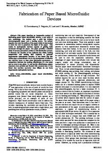
Fig. 5. Photograph of the microdevice after bonding and prior to sealing.
shortest and highest slots in PDMS are ca. 170 and ca. 510 μm respectively, while that of the intermediate slot is ca. 340 μm. Portions of the SU-8 structures, corresponding to vertical holes in PDMS, at the end of two of the SU-8 structures, corresponding to slots in PDMS, are visible in Fig. 4c. The next step in the process layout is the casting of PDMS. The prepolymer is mixed with a curing agent (10:1 W/W) following which the mixture is degasified and poured on top of the wafer until the patterns are submerged. Following this, the mold along with the holder is heated for a period of 2 h, on a hot plate at 125 °C, to cure the PDMS. Afterwards, the solidified PDMS is peeled off from the mold and diced into desired shape. The PDMS substrate has a microchannel as well as three slots, for holding the microelements, and vias. The height of the microchannel is ca. 510 μm while its width is 300 μm. The microchannel and the slots can be accessed from the face that forms the interface between the PDMS and SU-8 mold. The manifolds of the microchannel are punched using a blunt needle to create vias through the PDMS substrate for linking the microchannel to the external fluidic components. In addition, vias are also created in the PDMS substrate above the vertical holes, mentioned earlier, at the ends of each slot. In the next step of the process layout, the microelements are placed inside each of the slots. The microelements are pushed into the slot until they rest against the bottom wall. Following this, the PDMS and glass substrates of similar planar are placed inside the plasma cleaner with bonding sides up. At about 65 mbar, the plasma is turned on. Thus, both parts of the microdevice are treated with oxygen plasma for two minutes. Oxygen plasma contains high energy species including
31
electrons, ions, and radicals that strongly oxidize, activate and clean the PDMS and glass surfaces. This treatment improves surface wettability, renders the surface hydrophilic and facilitates the PDMS and glass bonding. The PDMS substrate is then bonded to the glass substrate by bringing the two plasma treated surfaces into contact. A slight pressure is applied to ensure a good seal. At this stage the microelements are completely embedded inside the microdevice. Fig. 5 is a photograph of the microdevice immediately after the completion of bonding. The vertical holes and the corresponding vias are clearly visible in the photograph; the vias above the vertical holes are open to the external environment. Though the elements are inserted into the slots, the technique is repeatable for the following reasons. As the length of the microelements is much greater than the width of the microchannel, and since only a small section of an element appears inside the microchannel, the desired horizontal alignment of the section inside the microchannel is easily achievable. Moreover, as the bottom surface of each slot acts as the seat of a microelement, it is possible to achieve accurate placement of each element at the desired depth within the microchannel. The next step in fabrication involves sealing of the sections of the slots on either sides of the microchannel in order to avoid any sample from entering them during operation. Each slot is sealed individually as it allows for more control over the process. Aged (ca. 6 h @ room temperature) liquid PDMS is introduced at the opening of the vertical hole on the top surface of the PDMS substrate corresponding to each slot from where it progresses by capillary action into the vertical hole and subsequently the corresponding slot. Fig. 6 shows a photograph of liquid PDMS seeping through the slot. When the moving meniscus of the liquid PDMS reaches the interface, between each slot and the microchannel, the capillary action is immediately terminated by manually covering the opening of the vertical hole with a small glass piece. The high viscosity of aged liquid PDMS is leveraged to control the progression of its meniscus. Afterwards, the microdevice is heated to cure the PDMS to permanently seal the slot. The glass piece that was used for covering the opening of the vertical hole is removed at this stage. By incorporating vias above the vertical holes in the PDMS substrate it is possible to fill each slot individually. 3. Conclusion We have introduced a novel and versatile method for fabricating PDMS-based microfluidic devices with integrated functional 3D microstructures for a broad range of applications. The method has been demonstrated via the fabrication of a device with multiple horizontally aligned prefabricated metallic microelements integrated lengthwise
Fig. 6. Photographs of the progression of meniscus of liquid PDMS through a slot; (a)–(c) progression of liquid PDMS, over the magnetic element, in the slot and (d) slot permanently sealed with cured PDMS. (1 is the PDMS structure, 2 is the microelement, 3 is the aged PDMS, and 4 is the main microchannel).
32
B. Mathew et al. / Microelectronic Engineering 187–188 (2018) 27–32
across the width of a microchannel and orthogonal to the flow. The 3D microelement structure is especially relevant for applications involving dielectrophoresis and magnetophoreis. It can be used to produce electric and magnetic field distributions across the entire height of the microchannel that provide particle manipulation and capture across the channel, with higher throughput than conventional microdevices. The process-layout includes standard microfabrication processes such as photolithography, casting, and bonding and therefore the fabrication process is easily reproducible with the same repeatability as that of these standard microfabrication processes. While the process layout is demonstrated for three metallic microelements, it can be extended to either include as many microelements of other materials as desired or create arrays of three-dimensionally arranged elements. Competing financial interests The authors declare no competing financial interests. Acknowledgement The authors gratefully acknowledge the funding from Al Jalila Foundation, Dubai, UAE for this work through their seed funding program, grant # AJF201618. References [1] D.R. Gossett, W.M. Weaver, A.J. Mach, S.C. Hur, H.T.K. Tse, W. Lee, H. Amini, D. Di Carlo, Label-free cell separation and sorting in microfluidic systems, Anal. Bioanal. Chem. 397 (8) (2010) 3249–3267. [2] I. Stiharu, A. Alazzam, V. Nerguizian, D. Roman, Single living cell manipulation and identification using microsystems technologies, Microsyst. Nanoeng. 1 (2015). [3] B. Mathew, A. Alazzam, S. Khashan, M. Abutayeh, Lab-on-chip for liquid biopsy (LoC-LB) based on dielectrophoresis, Talanta 164 (1) (2016) 608–611. [4] A. Alazzam, B. Mathew, F. Alhammadi, Novel microfluidic device for the continuous separation of cancer cells using dielectrophoresis, J. Sep. Sci. 40 (5) (2016) 1193–1200.
[5] S. Khashan, A. Alazzam, E. Furlani, Computational analysis of enhanced magnetic bioseparation in microfluidic systems with flow-invasive magnetic elements, Sci. Rep. 4 (2014). [6] B.Y. Park, M. Madou, 3-D electrode designs for flow-through dielectrophoretic systems, Electrophoresis 26 (19) (2005) 3745–3757. [7] J. Voldman, M.L. Gray, M. Toner, M.A. Schmidt, A microfabrication-based dynamic array cytometer, Anal. Chem. 74 (16) (2002) 3984–3990. [8] L. Wang, L. Flanagan, A.P. Lee, Side-wall vertical electrodes for lateral field microfluidic applications, J. Microelectromech. Syst. 16 (2) (2007) 454–461. [9] S. Li, M. Li, Y.S. Hui, W. Cao, W. Li, W. Wen, A novel method to construct 3D electrodes at the sidewall of microfluidic channel, Microfluid. Nanofluid. 14 (3–4) (2013) 499–508. [10] Y. Kang, B. Cetin, Z. Wu, D. Li, Continuous particle separation with localized ACdielectrophoresis using embedded electrodes and an insulating hurdle, Electrochim. Acta 54 (6) (2009) 1715–1720. [11] A. Pavesi, F. Piraino, G.B. Fiore, K.M. Farino, M. Moretti, M. Rasponi, How to embed three-dimensional flexible electrodes in microfluidic devices for cell culture applications, Lab Chip 11 (9) (2011) 1593–1595. [12] S.V. Puttaswamy, P. Xue, Y. Kang, Y. Ai, Simple and low cost integration of highly conductive three-dimensional electrodes in microfluidic devices, Biomed. Microdevices 17 (1) (2015) 1–5. [13] T. Müller, G. Gradl, S. Howitz, S. Shirley, T. Schnelle, G. Fuhr, A 3-D microelectrode system for handling and caging single cells and particles, Biosens. Bioelectron. 14 (3) (1999) 247–256. [14] M. Li, S. Li, J. Wu, W. Wen, W. Li, G. Alici, A simple and cost-effective method for fabrication of integrated electronic-microfluidic devices using a laser-patterned PDMS layer, Microfluid. Nanofluid. 12 (5) (2012) 751–760. [15] K.-H. Han, A.B. Frazier, Continuous magnetophoretic separation of blood cells in microdevice format, J. Appl. Phys. 96 (10) (2004) 5797–5802. [16] T. Lund-Olesen, M. Dufva, M.F. Hansen, Capture of DNA in microfluidic channel using magnetic beads: increasing capture efficiency with integrated microfluidic mixer, J. Magn. Magn. Mater. 311 (1) (2007) 396–400. [17] J. Jung, K.-H. Han, Lateral-driven continuous magnetophoretic separation of blood cells, Appl. Phys. Lett. 93 (22) (2008) 223902. [18] D.W. Inglis, R. Riehn, R. Austin, J. Sturm, Continuous microfluidic immunomagnetic cell separation, Appl. Phys. Lett. 85 (21) (2004) 5093–5095. [19] M. Faivre, R. Gelszinnis, J. Degouttes, N. Terrier, C. Riviere, R. Ferrigno, A.-L. Deman, Magnetophoretic manipulation in microsystem using carbonyl iron-polydimethylsiloxane microstructures, Biomicrofluidics 8 (5) (2014), 054103. [20] R. Afshar, Y. Moser, T. Lehnert, M.A. Gijs, Magnetic particle dosing and size separation in a microfluidic channel, Sensors Actuators B Chem. 154 (1) (2011) 73–80. [21] Microchem, SU-8 2000 Datasheet, www.microchem.com 2016.