M3E.2.pdf
OFC 2014 © OSA 2014
Fast Dynamic Wavelength and Path Scheduling in a Monolithic 8×8 Switch Q. Cheng1, R. Stabile2, A. Rohit2, A. Wonfor1, R. V. Penty1, I. H. White1 and K.A. Williams2
1
Centre for Photonic Systems, Electrical Division, Department of Engineering, University of Cambridge, United Kingdom 2 COBRA Research Institute, Eindhoven University of Technology, Eindhoven, The Netherlands Author e-mail address:
[email protected]
Abstract: The control plane is implemented for the first time to allow scheduling and power leveling in a monolithic 8×8 space and wavelength selective cross-connect. 16 dynamic data connections are established within 16µs. OCIS codes: 130.6622 Subsystem integration and techniques, 130.4815 Optical switching devices
1. Introduction The relentless scaling in required network bandwidth combined with the highly bursty nature of traffic in computer networks and data centers is leading to renewed interest into high-bandwidth, packet-compliant, optically-switched interconnects. So far the connectivity required for optical switches in such applications has far outstripped the capability of demonstrated packet-compliant photonic systems. However, the combination of wavelength domain wavelength selective switching and space domain photonic switching offers a powerful route to much higher connectivity [1]. The OSMOSIS architecture demonstrated 64 way connectivity using eight WDM input connections, and a multi-stage implementation is projected to scale to a thousand ports [2]. The use of discrete photonic components in such demonstrators has however been prohibitive in the numbers of fiber connections, component numbers and overhead in terms of assembly, calibration, synchronization, management and energy use. The recent integration of an eight port wavelength and space selective switch allows for much of this complexity to be contained within one single 14mm × 6mm chip [3, 4]. Extensive photonic integration means that all switch states may be synchronized, allowing considerable reductions in control complexity, calibration, and an improved control of optical losses. In this work, we now implement a control plane for the first time to demonstrate simultaneous dynamic routing in both wavelength and space domain on a monolithically integrated photonic chip. Sixteen unique data connections are implemented within a time period of 16 µs by uploading the Round Robin schedule to the FPGA switch controller. Automated routing is demonstrated for four wavelengths from each of four inputs to one output and automated measurements are performed verify connectivity.
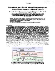
Fig. 1 Photograph of the 8×8 wavelength and space switch.
2. Device details A photograph of the 8×8 cross-connect is shown in Fig. 1. The switching circuit is a synchronous broadcast-andselect photonic space switch with wavelength granularity routing. This is implemented with semiconductor optical amplifier gates. Up to eight independent wavelengths may be carried on each of eight fibers to achieve sixty-fourway distribution. The shuffle network is fully integrated to minimize the numbers of optical fiber connections and radically reduce time-of-flight delays. Wavelength domain switching is implemented with a second stage of wavelength selective switches based on a cyclic router, SOA gates and a broadband fan-in. The architecture and routing map is detailed for the case of an earlier and smaller 4×4 prototype [1]. Any input wavelength from any
M3E.2.pdf
OFC 2014 © OSA 2014
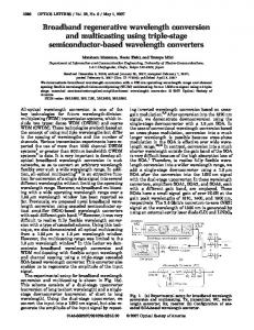
input connection can be routed to any output through the appropriate biasing of two SOA gates. A FPGA is then programmed to sequence the on/off states on selected SOA gates for optical path routing. 3. Control plane The switch fabric includes a PC-interfaced control plane which comprises an Altera Stratix III FPGA for timing control with transition times of 4ns and a microcontroller-based level controller for setting the on-state bias currents. A 50MHz signal generator is used to synchronize the pulse pattern generator with the FPGA. The FPGA is primarily used for controlling the optical switch, and additional digital pins are used for test equipment control. A Stanford delay generator is used to condition one such test control signal from the FPGA to the gate input of the error detector for path-dependent BER measurement. Custom current driver boards interface the level and timing control signals to generate the nanosecond transient current signals to the optical switch. A schematic of the control plane is shown by Fig. 2. The control signals from eight of the FPGA digital output pins are shown schematically at the bottom of the image for space selection and wavelength selection. Four Santec tunable laser modules are operated at the wavelengths 1555.94, 1552.76, 1549.56 and 1545.69 nm respectively, named from λ0 to λ3, which are multiplexed using an arrayed-waveguide-grating (AWG). A one-tofour way electrical delay generator is used between the pattern generator and the four optical modulators to decorrelate the wavelengths carrying the 10Gb/s pseudorandom bit sequences (PRBS) signals. The multiplexed data is amplified by the same Erbium doped fibre amplifier (EDFA) and split four ways. Different lengths of fiber are also introduced between the 1×4 fiber splitter and the input ports of the switch fabric for decorrelating signals. A polarization controller is set for each of the four ports. 10Gb/s PPG
50MHz clock
AWG
Coupler
PCs
MZMs
FPGA
control
λ0, λ1, λ2, λ3 λ0, λ1, λ2, λ3 λ0, λ1, λ2, λ3 8 x 8 wavelength & λ0, λ1, λ2, λ3
EDFA
Delay gen
Computer
Manual current Control for pre-amp
Electrical Amplifier
Lasers
Current
Slash denotes multiple lines
GPIB
EDFA 90:10 coupler
Space Switch
PCs
10Gb/s error detector
AWG
1:4 Delay gen
Guard band
Output 3
Receiver
Power meter
Payload
Space select stage
I0
I1
I2
I3
I0
I1
I2
I3
I0
I1
I2
I3
I0
I1
I2
I3
I0 I4
…
Wavelength select stage
λ0
λ0
λ0
λ0
λ1
λ1
λ1
λ1
λ2
λ2
λ2
λ2
λ3
λ3
λ3
λ3
λ4 λ0
…
Gate signal
Time trace
Sweep
Fig. 2 Schematic of control plane for the dynamic space- and wavelength- routing. The time trace for FPGA control and gate signals are presented at the bottom.
The routed packet has a payload of 940 ns followed by a 60 ns guard band, defining an overall time-slot of 1 s. The input data sequence is 213-1 pseudo-random bit sequence which is repeated to fill the time slot. The switch scheduler sequences sixteen paths periodically within a time period of 16 µs, as illustrated at the bottom of Fig. 2. Four wavelengths from four ports are directed sequentially to one output. The routed packets from output O3 are amplified by an EDFA and filtered by an AWG. A dc-coupled lightwave converter (HP11982A) is connected to the 10-Gb/s error detector. While this is not a burst mode receiver, and does lead to compromised detection, it allows for preliminary assessment of the switching fabric. The BER measurement is automatically performed by repeatedly polling the error detector and recording values on the computer, for a range of DC decision threshold values and path configurations. The optimized timing for each measurement can be adjusted via the 1:4 electrical delay generator at the optical transmitters in Fig. 2. The error-rate is measured for one time slot at a time by using a control signal generated by the FPGA to mask out one channel. This selected time slot is scanned at a time scale of minutes to allow the polling of error rate for each dynamic path. Within each gating period, the BER is measured every 16 µs and updated every 3 seconds. 4. Dynamic wavelength- and space-routing A constant current of 40 mA is injected to the pre-amplifiers, while an on-state current of 45 mA is set for both the wavelength and space selecting SOA gates in the microcontroller. The off-state current is measured to be below
M3E.2.pdf
OFC 2014 © OSA 2014
5mA. The gate signal is swept from the first packet to the 16th in one 16µs time-cycle, allowing path studies for all 16 dynamic connections. BER measurement reveals that five connections already operate error free without an optimized burst mode receiver. Detailed BER measurements will be presented at the conference. Dynamic eye diagrams for the 16 channels are captured and shown in Fig. 3. The voltage levels for the different eye diagrams show an 8dB path dependence loss. It can be seen from Fig. 3 that some paths are over-biased, resulting in high power but with a broadening in the high level, while some paths are under-biased, causing low power level. Nonetheless, a clear opening is observed for the range of routed paths. λ0
λ1
λ2
λ3
Path 0-3 50mV/div
50mV/div
50mV/div
50mV/div
50mV/div
25mV/div
25mV/div
50mV/div
50mV/div
50mV/div
50mV/div
25mV/div
50mV/div
50mV/div
50mV/div
50mV/div
DC level
Path 1-3 Path 2-3
Path 3-3 Fig. 3 Dynamic eye diagrams of 10Gb/s data for 16 connections, 4 wavelengths from 4 input ports to one output port.
The time trace for all sixteen connections, are shown in Fig. 4 to highlight the varying output power levels for the different paths when 45mA is applied to each on-state SOA gate. The differing levels of path dependent gain and loss can however be compensated directly. Power equalization is subsequently performed by individually optimizing the current levels at each of the SOA gates. In this experiment, the levels are set by a slower microcontroller: onstate levels are optimized for the different electrodes, but these cannot be changed between time intervals for the implemented control hardware. As each SOA gate is responsible for multiple connections, the power is not perfectly leveled but it can be reduced to 2dB which should allow good operation with a burst mode receiver. Dynamic power leveling may be implemented to further optimize the power equalization. Input
3 0 1 2 3 0 1 2 3 0 1 2 3 0 1 2
Input
3 0 1 2 3 0 1 2 3 0 1 2 3 0 1 2
Power Equalization
λ3
λ0
λ1
λ2
λ3
λ3
λ0
λ1
λ2
λ3
Fig. 4 Power trace for the 16 connections with and without static power equalization
4. Conclusion We have implemented Round Robin scheduling to dynamically connect sixteen unique paths within sixteen microseconds across a highly integrated monolithic 8×8 cross-connect. The first quantitative analysis is performed under dynamic multi-connection routing on a data packet time-scale. 5. References [1] A. Rohit, J. Bolk, X.J.M. Leijtens, K.A. Williams, "Monolithic nanosecond-reconfigurable 4x4 space and wavelength selective crossconnect", Journal of Lightwave Technology, 30 , 17, 2913-2921, (2012) [2] R. Hemenway, R.R. Grzybowski, C. Minkenberg and R. Luijten, "An optical packet-switched interconnect for supercomputer applications", Invited paper, Journal of Optical Networking, Special Issue on Supercomputer Interconnects, 3, 11, 900–913, 2004 [3] A. Rohit, R. Stabile, K.A. Williams, "8×8 space and wavelength selective cross-connect for simultaneous dynamic multi-wavelength routing", Invited Paper, Proceedings OFC, OW1C.4 (2013) [4] R. Stabile, A. Rohit, K.A. Williams, "Dynamic multi-path WDM routing in a monolithically integrated 8x8 cross-connect", Proceedings ECOC, We4B2 (2013)