102
IEEE TRANSACTIONS ON COMPUTER-AIDED DESIGN OF INTEGRATED CIRCUITS AND SYSTEMS, VOL. 23, NO. 1, JANUARY 2004
Fast Postplacement Optimization Using Functional Symmetries Chih-Wei (Jim) Chang, Ming-Fu Hsiao, Bo Hu, Kai Wang, Malgorzata Marek-Sadowska, Fellow, IEEE, Chung-Kuan Cheng, Fellow, IEEE, and Sao-Jie Chen
Abstract—The timing-convergence problem arises because estimations made during logic synthesis may not be met during physical design. In this paper, an efficient rewiring engine is proposed to explore maximal freedom after placement. The most important feature of this approach is that the existing placement solution is left intact throughout the optimization. A linear-time algorithm is proposed to detect functional symmetries in the Boolean network which are then used as the basis for rewiring. Integration with an existing gate-sizing algorithm further proves the effectiveness of our technique. Three applications are demonstrated: delay, power, and reliability optimization. Index Terms—Functional symmetry, logic restructuring, logic synthesis, physical synthesis, postlayout optimization, timing closure.
I. INTRODUCTION
I
N THIS PAPER, we present a technique focusing on the identification of symmetries when the target Boolean function is represented as a mapped Boolean network. In general, when two wires are functionally symmetric, they can be swapped without changing the overall circuit functionality. We have established a relationship between implication supergate [24] and functional symmetry. Based on our analysis of supergates, we propose a linear-time algorithm for symmetry identification in a multilevel netlist. We have developed efficient postplacement performance-improvement algorithms which apply symmetry-based rewiring and gate sizing. Power consumption and speed are two primary cost functions in today’s integrated circuit design. As mobile computation devices prevail in the market, the ability to design fast, low-power devices is of paramount importance. However, these two objectives often conflict: a faster circuit consumes more power, but a low-power circuit runs slower. Hence, designers often need to tradeoff power for speed and vice versa to meet the desired specifications. To get the best performance, power and speed
Manuscript received August 24, 2001; revised February 25, 2002, July 9, 2002, and March 7, 2003. This paper was recommended by Associate Editor M. Sarrafzadeh. C.-W. Chang is with Cadence Design Systems, San Jose, CA 95134 USA (e-mail:
[email protected]). M.-F. Hsiao is with the Faraday Technology Corporation, Sunnyvale, CA 94085 USA. B. Hu, K. Wang, and M. Marek-Sadowska are with the Department of Electrical and Computer Engineering, University of California, Santa Barbara, CA 93106 USA. C.-K. Cheng is with the Department of Computer Science and Engineering, University of California, San Deigo, La Jolla, CA 92093 USA. S.-J. Chen is with the Department of Electrical Engineering, National Taiwan University, Taipei 106, Taiwan. Digital Object Identifier 10.1109/TCAD.2003.819904
are considered at various stages of the design cycle, including architecture, register-transfer level, gate, and layout levels. Circuit reliability is another emerging design consideration. Design trends, such as device miniaturization, system-on-a-chip integration, and higher operating frequencies, increase concerns about circuit reliability. Hot-carrier effect (HCE) is one of the major failure mechanisms affecting long-term reliability. As the device dimensions shrink to the deep submicron ranges, the electric field in a transistor’s channel increases significantly. Electrons and holes traveling in the channel may gain high enough kinetic energy to be injected into the gate oxide and cause permanent changes in the oxide-interface charge distribution. In an NMOS transistor, HCE leads to transconductance degradation, shift in the threshold voltage, and decrease in the drain-current driving capability. The performance degradation of particular devices leads to degradation in the overall circuit performance. The transistor degradation behavior is a function of time, the number of transitions, its fanins’ driving capability, and geometric dimensions. The effects accumulate while the device is in operation. As a result, circuits age. Our proposed rewiring technique will be used to target delay, power, and reliability optimization specifically at the postplacement level when the gate level netlist is already placed on a twodimensional plane. The rationale behind this methodology is that delay, power, and reliability cannot be determined without physical information. The optimization effort could be misled by inaccurate estimation of the objective function. However, since the placement is already done, optimization techniques used at this level must not perturb the existing placement solution too much, in order to guarantee timing closure. Buffer insertion and gate sizing are traditionally the only two techniques that are suitable for this purpose. However, these two techniques are limited to the existing netlist, not enabling us to explore a larger solution space by restructuring the logic. In recent years, rewiring techniques, such as redundancy-addition-and-removal [11] have been successfully applied at postlayout stages to restructure the logic. This technique has the property that only wires are reconnected without disturbing the existing placement solution. This important property allows logic changes to be guided by accurate delay information. Our proposed functional symmetry-based rewiring technique explores another degree of freedom compared with the existing techniques. II. PRELIMINARIES A Boolean network [1] is a directed acyclic graph (DAG) , where is the set of vertices and is the set
0278-0070/04$20.00 © 2004 IEEE
Authorized licensed use limited to: National Taiwan University. Downloaded on February 3, 2009 at 22:42 from IEEE Xplore. Restrictions apply.
CHANG et al.: FAST POSTPLACEMENT OPTIMIZATION USING FUNCTIONAL SYMMETRIES
of edges connecting vertices. Let be a vertex in . The (immediate) fanout of is a set of nodes such that there is an edge from to . Similarly, the (immediate) fanin of is a set of nodes , such that there is an edge from to . A node is called an internal node if it is neither a primary input (PI) nor a primary output (PO). The fanout cone of , or transitive fanout of , is a set of nodes , such that there exists a directed path from to . Similarly, the fanin cone of , or transitive fanin of , is a set of nodes such that there exists a directed path from to . The terms “vertex” and “node” are used interchangeably. Each vertex has a function associated with it. Function maps the Boolean space spanned by its fanins to the space spanned by its fanouts. In practice, we are interested only in the case when is a single-output function. All fanouts of are fed by the same . Even though is a single-output function, the number of fanouts of can be more than one. be a library of logic gates. A Boolean network is Let mapped when the function associated with each vertex is implemented by a gate from . Otherwise, it is unmapped. Let be a gate in . An in-pin of is the connector of to which outputs of other gates can connect. An out-pin of is the connector that can drive other gates’ in-pins. The logic type of is denoted type . We do not distinguish between the name of a gate and its out-pin. Let be a fanout-free network rooted at . By fanout-free, we mean that each node inside has only a single fanout. A path is an alternating sequence of pins and gates such that for any two consecutive gates the former is driving the latter. For starts from the example, a path of gate .A in-pin of gate and ends at the in-pin path is fanout-free if all gates along the path are fanout-free. An input to a gate on the path is a side input if the gate driving is not on the path. Definition 1: An input-controlling value of an in-pin of a gate , denoted , is the logic value which, when set at , uniquely determines the output of regardless of the logic values on other inputs. An output-controlled value of a gate , , is ’s output value when one of its input pins denoted is set to its input controlling value. NAND, the input-controlling For example, when type value of an in-pin of is 0, and output-controlled value of is 1. For buffers and inverters, both 0 and 1 are input-controlling values, since they uniquely determine the output. The input-controlling value of the in-pins of an exclusive-or (XOR) gate is undefined since no logic value at any single input can uniquely determine the output. In this case, the output controlled value is also undefined. Definition 2: An output noncontrolled value of the gate , , is the logic value which, when set at the output denoted of , uniquely implies the logic values at the inputs of . An input noncontrolling value of an in-pin of , denoted , is the logic value inferred when the output of is set to its output noncontrolled value. For example, when type NAND, the output noncontrolled value of is 0, since a 0 at ’s output uniquely implies that all inputs to have to be set to 1, the input noncontrolling value. For buffers and inverters, both 0 and 1 are output noncontrolled values since they also imply the only input’s logic value. The
103
output noncontrolled value and input noncontrolling values are undefined for exclusive-or gate. Logic implication is a process of inferring consistent logic values based on known logic values. Given a logic value assigned at the out-pin of gate , the direction of implication can be forward or backward, until no more logic values can be in, all in-pins of can be inferred with ferred. If logic value . This process is called direct backward imAND and . All in-pins plication. For example, let type of are inferred with logic value 1. Direct backward implication stops at a gate when the value assigned at the out-pin of is not equal to and hence no logic value at the is the value in-pins of can be further inferred. set at a pin during direct backward implication. Let be an ordered list of nodes from a Boolean network. If is not in the transitive fanout cone for any preceding in of , then is in a topological order. is in reverse topological order if for any , in , is not in the transitive fanin cone of . We will use the following two types of symmetries. and are nonequivalence symmetric Definition 3: if and only if . That is, (NES) [8] in . By plugging in all four possible value combinations to and in the above equation, we can derive the following four relationships:
The first and fourth relationships are clearly tautological. Hence, for and to be NES, the cofactors and have to be equivalent. The name “nonequivalence symmetric” was derived from the fact that in the second and third relationare of opposite logic values. ships, and and are equivalence symmetric Definition 4: if and only if . That is, (ES) [8] in . Again, we could plug in all four possible value combinations to and in the above equation and derive the following four relationships:
This time, the second and third relationships are tautological. Hence, for and to be ES, the cofactors and have to be equivalent. The name “equivalence symmetric” was derived from the fact that in the first and fourth relationships, and are of the same logic values. Definition 5: and are symmetric in if they are . That is, when the distinction between either NES or ES in NES and ES is not of importance in the context, we use the term “symmetric” to mean the relationship is either NES or ES.
Authorized licensed use limited to: National Taiwan University. Downloaded on February 3, 2009 at 22:42 from IEEE Xplore. Restrictions apply.
104
IEEE TRANSACTIONS ON COMPUTER-AIDED DESIGN OF INTEGRATED CIRCUITS AND SYSTEMS, VOL. 23, NO. 1, JANUARY 2004
Detecting symmetry has long been an active area of research in switching theory. In [16], necessary conditions for the existence of symmetry in a completely specified Boolean function are identified using the structural properties of ROBDD [1]. Chang et al. [4] present an extension to handle incompletely specified functions. In [19], symmetry detection is transformed into a test generation problem and solved using automatic test pattern generation (ATPG) techniques. We briefly review some terminology used in test generation. After a chip has been designed and fabricated, it must be tested to determine whether it is working correctly. This is done by applying input vectors and then capturing and analyzing the output vectors may be response. For a sequential circuit, up to tested, where is the number of primary inputs and is the number of flip-flops. Applying all of the possible input vectors may take too much time. The single stuck-at-fault model assumes that the physical defects manifest themselves as wires, which are permanently connected to either V or GND, and that only one such stuck-at wire exists in a given circuit. from a node For the single stuck-at-fault model, a wire to a node could be stuck at either 1 or 0. Let be a multiple-input multiple-output Boolean function implemented and by a combinational circuit C. The functions are implemented by the faulty and good circuits, respectively. We use the D-notation [21] to represent the fault effect. D (1/0) means that in the good circuit, the value of a particular wire is 1 whereas in the faulty circuit the value of the same wire is 0. denotes the opposite case. The fault on is testable if there . exists a primary input vector such that That is, the difference between the good and faulty circuits can be observed at primary outputs when the primary input vector is applied. When no vector exists, which can distinguish the faulty circuit from the good one, the fault on is redundant and can be removed by assigning the constant stuck-at-value on . The process of finding such a vector through algorithmic means is called automatic test pattern generation (ATPG). The processes of test generation and redundancy identification are known to be NP-hard. In test generation, each node in the network could assume one of five different logic values which are 0, 1, , , or unassigned. Logic operations work in a bit-wise fashion. For example, the logic-OR operation (+) between 1 and D can be determined from the individual operations in the good and faulty circuits, that is, 1 1 in the good circuit, and 1 0 in the faulty circuit. The result is 1 in the good circuit, and 1 in the faulty . Other operations can be similarly circuit. In short, deduced. We now reiterate the main results of [19] in the following lemma. Lemma 1: Two inputs and are of NES if and only if no test exists that sets to D, sets to , and propagates D or to the output of . Furthermore, and are of ES if and only if no test exists that sets to D, sets to D, and propagates D or to the output of . Here we assume is represented as a mapped Boolean network. Lemma 1 simply conveys Definitions 3 and 4 from the viewpoint of test generation. For example, when no D or can propand , it means the agate to the output of when
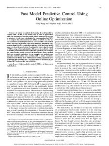
0
h
f
0
k 1
0
(a)
0
h
f
0
k 1
0
(b) Fig. 1.
h and k are swappable.
function is indistinguishable from the function , which is exactly Definition 3. Lemma 1 establishes the link between the theory of test generation and the traditional definition of functional symmetry. All previous attempts at symmetry detection have focused on finding symmetries in the primary inputs of a given function. be a multiple-input, multiple-output Let repreBoolean function defined on sented by a mapped Boolean network . Also, let be a and let be the corresponding single-output subnetwork of , where Boolean function defined on is a set of internal signals of . Instead of finding symmetries with respect to , we focus on the identification for , with respect to . The number of symmetries for , of detected symmetries increases dramatically since is only a subfunction of . This analysis forms the basis of our rewiring technique. Symmetries detected inside a Boolean network immediately provide ways to restructure the network for better performance. In Fig. 1(a), if we know and are symmetric, they can be swapped without changing the overall circuit functionality. Depending on the optimization goal, one of the two circuits might be better than the other. We now present our approach to detect functional symmetries inside a Boolean network. III. DETECTION OF SYMMETRIES IN A NETWORK In this section, we use the theory of ATPG as a tool for the proofs. Our algorithm does not use ATPG. A. Symmetry Detection Let be a fanout-free network rooted at . Let and be two in-pins in as illustrated in Fig. 2. Since is fanout-free, there exists a unique path from to , where p is an in-pin of . Similarly, there exists a unique path from to , where is and for an in-pin of . We use the notation these two paths, respectively. All of the following lemmas and
Authorized licensed use limited to: National Taiwan University. Downloaded on February 3, 2009 at 22:42 from IEEE Xplore. Restrictions apply.
CHANG et al.: FAST POSTPLACEMENT OPTIMIZATION USING FUNCTIONAL SYMMETRIES
a
TABLE I VALUE ASSIGNMENT WHEN type(f ) =AND
p f
value(p) value(q)
q
b Fig. 2. Two unique paths in a fanout-free network.
pi pj
gj
pi
(a) Fig. 3.
105
gj pj
implied value(f)
satisfies
D
D
D
Condition 1
D
D
D
Condition 1
1
D
D
Condition 2
1
D
D
Condition 2
D
1
D
Condition 2
D
1
D
Condition 2
(b)
(a) AND-OR reachability. (b) XOR reachability.
theorems in this section are considered under the assumption that the underlying structure is fanout-free. We also assume that and do not properly contain each other. be an in-pin of a gate and be a Definition 6: Let gate in the fanout cone of . is a path to . is AND-OR-reachable from , if has an from inferred logic value via direct backward implication when is . is XOR-reachable from if all gates along P set to (including ) are of type either XOR, INV, or BUF, with at least one gate of type XOR. Since an XOR gate has no controlling value, it is clear that is these two definitions are mutually exclusive. That is, if AND-OR-reachable from , it cannot be XOR-reachable from . Also, if is XOR-reachable from , it cannot be AND-OR-reachable from . Fig. 3 illustrates the definition of AND-OR and XOR reachability. In Fig. 3(a), when the output of is set to 1, it implies to 1, which further infers a 0 through the inverter. The backward implication ends at with a 1 implied. By definition, we say is AND-OR reachable from . In Fig. 3(b), the path from to consists of an XOR gate followed by two XNOR gates. An XNOR gate can be viewed as an XOR gate followed by an inverter. Since all gates on the path are of either XOR or INV, is XOR-reachable from by definition. In order to detect symmetries of two pins ( , ) with respect to , consider the case when is assigned D and is assigned . We use to denote the logic value assigned at pin and value . Lemma 2: Let be AND-OR-reachable from the gate with is set to D, it is logically inconsistent input pin . When value is set to . That is, when value is set to D, if value cannot be set to . value Proof: Assume value is assigned . Since is AND-OR-reachable from , assigning at results in either 0 or 1 being implied at , depending on the number of inversions along the path. This is in conflict with being assigned D initially. By contradiction, value cannot be set to . . Take Fig. 3(a) as an example. is AND-OR reachable from . Let a logic value D be set at . At , if we set a logic value 1, which is the input noncontrolling value of the in-pin , it immediately implies a 1 at . This would contradict the fact
that a D has already been set at . As a result, when we set a D at the input pin . at , we cannot set an be XOR-reachable from gate and Lemma 3: Let value , value can only be either D or . and , it is clear that Proof: Since the propagation of D (or ) from can only be inverted along is either D or , depending on the the path. That is, value number of inversions and value assignments on the side inputs cannot be assigned to 0 or 1. . along the path; value is D or depends on the In Lemma 3, whether value number of inversions and side input assignments along the path. Note that this condition differs from that of Lemma 2, where is D or depending only on the number of inversions value along the underlying path. Lemma 4: Consider a fanout-free network rooted at . Let be neither AND-OR-reachable nor XOR-reachable from gate and value ; can always be assigned 0 or 1. Proof: We first assume there exists no XOR gate along the . Since is not AND-OR-reachable, direct path backward implication from stops before reaching the pin . Under the assumption that the underlying structure is fanoutfree, the propagation of D from can always be stopped at the gate where direct backward implication from stops. Hence of either 0 or 1 is always justifiable. In the case when is not there exists an XOR gate along the path, since XOR-reachable, there exists at least one AND/OR gate along the path. The propagation of D from can always be stopped by assigning the side input pin of with . This assignment is also justifiable because is fanout-free. Hence, being 0 or 1 is also justifiable. . We now discuss the conditions on pin and pin such that a fault effect D or can appear at the output of the gate . {AND, OR}, we have the following two First, when type conditions. Condition 1: Both value and value are D or both are . and value is assigned their Condition 2: One of value corresponding input noncontrolling value and the other is D or . Table I lists value assignments on pin and such that either a D or is implied at the output of , when type AND. Other and value , or value assignments, such as value and value , imply constant logic value 0 value at the output of . Second, when type {XOR}, the condition on pin and pin becomes the following.
Authorized licensed use limited to: National Taiwan University. Downloaded on February 3, 2009 at 22:42 from IEEE Xplore. Restrictions apply.
106
IEEE TRANSACTIONS ON COMPUTER-AIDED DESIGN OF INTEGRATED CIRCUITS AND SYSTEMS, VOL. 23, NO. 1, JANUARY 2004
Condition 3: Only one of value and value is D or ; the other can be either 0 or 1. and value , the For example, when value output at gate is . On the other hand, when Condition 3 is and value not satisfied, such as the case when both value are D, the output is a constant logic value. If Conditions 1 and 2 fail when the type of is either AND or OR, or Condition 3 fails when is XOR type, there exists no consistent value assignment that can propagate either a D or , to the output of . This situation, by Lemma 1, implies ( , ) are symmetric with respect to . A direct consequence of Lemma 4 is the following. be neither AND-OR-reachable nor Lemma 5: Let XOR-reachable from a gate ; then ( , ) is not symmetric with respect to . is set to D, it is always possible Proof: When value to propagate this value to such that value is either D or , since the underlying structure T is fanout-free. Whether the value at is D or depends on the number of inversions along the path from to . From Lemma 4, we know that value can be assigned either 0 or 1 when is neither AND-OR-reachAND, we able nor XOR-reachable from gate . When type to 1, which is the of . Similarly, we can assign value can assign value to 0, when type OR and to either 0 or 1, XOR. In any case, either Condition 2 or Condiwhen type tion 3 is satisfied and hence ( , ) is not symmetric with respect . to . An important result is stated in the following theorem. realized as a Theorem 1: ( , ) are symmetric in fanout-free network if and only if and are AND-OR-reachable from the root of or and are XOR-reachable from the root of . Proof: The proof of the if part is trivial and, hence, omitted. We prove that if ( , ) are symmetric in , then and are AND-OR-reachable or XOR-reachable from the root of . From Lemma 5, we know that if and are not both AND-OR-reachable nor XOR-reachable, ( , ) cannot be symmetric. By the law of contraposition, we conclude that and are both AND-OR. reachable or XOR-reachable if ( , ) are symmetric. The importance of Theorem 1 is twofold. First, it expresses functional symmetry in terms of AND-OR, XOR reachability in a fanout-free network. Second, it provides the theoretical foundation for an efficient linear time algorithm for symmetry detection. Generally speaking, the condition of AND-OR and XOR reachability leads to the identification of NES and ES among the input pins. Knowing NES and ES directly allows us to swap pins with or without adding inverters. Details of the algorithm will be presented in the next section. B. Generalized Implication Supergate (GISG) To improve the efficiency of the test generation process, implication supergate extraction has been proposed by Tsai et al. in [24]. The extraction starts by assigning output noncontrolled value to each of the primary outputs, and direct backward implications are performed as far as possible. Gates at which implications stop are called implication supergate roots and are as-
1 g
f 0
Fig. 4.
Implication conflicts at the fanout stem.
signed their corresponding output noncontrolling value to start another round of direct backward implication. The gates that are reached by the same round of direct backward implication form an implication supergate rooted at the output of the gate from which the process has begun. The concept of implication supergate is extended in the following definition: Definition 7: Let T be a fanout-free subnetwork of N rooted at gate . A GISG of is the set of gates in T that are either AND-OR-reachable or XOR-reachable from . A gate is covered . An in-pin is covered by the GISG rooted at if by a GISG if the gate to which it is attached is covered by the GISG. The boundary-in-pins of a GISG are the in-pins covered by whose fanins are neither AND-OR-reachable nor the XOR-reachable from the supergate’s root . Here, the original definition of an implication supergate [24] has been extended to include XOR gates. Even though the property of AND-OR and XOR reachability can cross multiple fanout points, we restrict GISG to fanout-free regions for the purpose of keeping symmetry detection easy. To extract the maximal GISG from a given netlist, we start from the primary outputs and process each gate in a reverse topological order. At each primary output, depending on its gate type, we attempt either direct backward implication or XOR propagation. Multiple-fanout nodes, or nodes where backward propagation stops, are treated as new GISG roots, and the propagation process continues. This procedure stops when all primary inputs are reached. After the extraction, the network is uniquely partitioned into AND, OR, and XOR supergates with inverters and buffers at their pins. Definition 8: In a GISG network, each gate represents a root in the extracted network which contains all nodes that are covered by the same round of backward propagation originating from this root. A GISG is trivial if it covers only one gate. The type of a GISG is the same as the type of its root. During GISG extraction, redundancy can often be easily found. We show two cases in the following. • Case 1: backward implication conflicts at a fanout stem (see Fig. 4) In this case, we can write the following propositions:
so, and . That is, the value of f is independent of the value of . This means the s-a-fault at g is untestable, and hence is redundant. • Case 2: backward implication does not conflict at a fanout . That is, . So, stem one of the fanout stems of is s-a-1 untestable and hence redundant (see Fig. 5).
Authorized licensed use limited to: National Taiwan University. Downloaded on February 3, 2009 at 22:42 from IEEE Xplore. Restrictions apply.
CHANG et al.: FAST POSTPLACEMENT OPTIMIZATION USING FUNCTIONAL SYMMETRIES
and Without loss of generality, assume . Equation (2) can be written as case when
1 g
107
f 1
Fig. 5.
in the
(3)
Implication agrees at the fanout stem.
. This in turn implies , which is the definition of ES. That is, when , then ( , ) are inverted swappable. Other value combinations of and can . be similarly proved. both be XOR-reachable Lemma 8: Let the in-pins and from the gate ; then and are both inverting and noninverting swappable. , , or , , Proof: By applying the inputs to will always have value combinations such as D and D, and , or D and , because XOR gates along the path can never stop the fault effect. In either case, no fault effect can be seen at the output of the . That is, inputs to XOR-reachable . gates are always both ES and NES. Fig. 1(a) shows an GISG rooted at . There, and . By Lemma 7, we know and are noninverting swappable. That is, they can be swapped without introducing inverters. This is shown in Fig. 1(b). In other words,
IV. SWAPPABLE PINS Definition 9: Let be an in-pin of and be an in-pin of in a mapped Boolean network . Assume that the out-pin of connects to and the out-pin of connects to . If conto does not change the functionality necting to and of , then and are noninverting swappable. If connecting through an inverter to and through an inverter to does not change the functionality of , then and are inverting swappable. The notion of noninverting and inverting swappable pins corresponds to NES and ES. When there is no ambiguity, we use “swappable” to denote both noninverting swappable and inverting-swappable. A. Identification of Swappable Pins The main purpose of the GISG extraction is to explore the functional symmetry inside a network. Equipped with the information of functional symmetry, we can find wires that can be exchanged without changing the functionality of the network. Lemma 6: If two in-pins and are covered by the same GISG rooted at and and do not properly contain each other, they are swappable. The reason for the nonproper containment constraint is as follows. Since the underlying structure is fanout-free, if one path properly contains the other, it implies that swapping of these two pins will create loops and hence cause malfunction. Take Fig. 3(a) as an example. Pins and are covered by the same GISG rooted at . However, the path from to is properly contained by the path from to . Swapping of these two pins will create a cycle in the circuit. In the following, we implicitly assume that target pins fulfill the nonproper containment constraint. Let the in-pin of a gate is AND-OR-reachable from the is the value set at during direct backgate . ward implication from . both be AND-OR-reachable Lemma 7: Let in-pins and from gate . If , then ( , ) , are inverting swappable. If then ( , ) are noninverting swappable. Proof: Assume the output noncontrolling value at is , , and . By definition of direct backward implication, we have
B. Cross-Supergate Swapping Previous theorems show that pins that are covered by the same GISG are symmetric and, hence, swappable. Further analysis shows that groups of pins belonging to different implication supergates may also be swappable. Definition 10: (DeMorgan transformation on an implication supergate) Let SG1 be an implication supergate and {AND, OR}. We define operator DeMorgan (SG1) as the addition of inverters to all inputs and the output of SG1. Theorem 2: Let SG1 and SG2 be two implication supergates. and are the sets of fanins to SG1 and SG2 and . If the outputs of SG1 and SG2 are sym{AND, OR}, metric and type(SG1) and type and are swappable under DeMorgan transformation of SG1 and SG2. Proof: Without loss of generality, assume type AND and type OR. Since output(SG1) and output(SG2) are symmetric, these two pins are swappable. However, instead of swapping these two pins, we can connect fanins(SG1) to DeMorgan(SG2) and connect fanins(SG2) to DeMorgan(SG1). That is, we make type(DeMorgan(SG2)) equal to type(SG1) and type(DeMorgan(SG1)) equal to type(SG2). If both SG1 and SG2 are of the same type, no DeMorgan transform is necessary. This swapping and transformation procedure clearly preserves . the functionality of the network. The example in Fig. 6 shows the process of cross-supergate swapping.
(1) By the law of contraposition, the above propositions can be rewritten as
(2)
V. DELAY OPTIMIZATION Two types of postplacement performance optimizations are made possible by exploiting GISGs. • Wire length reduction: Fig. 7(a) shows a set of placed gates and two signals and coming from geometrically fixed
Authorized licensed use limited to: National Taiwan University. Downloaded on February 3, 2009 at 22:42 from IEEE Xplore. Restrictions apply.
108
IEEE TRANSACTIONS ON COMPUTER-AIDED DESIGN OF INTEGRATED CIRCUITS AND SYSTEMS, VOL. 23, NO. 1, JANUARY 2004
De Morgan transform
We use a load-dependent model for gate delay. The delay from an input pin to an output pin is
d e g SG1
a b c
a
Here, is the load capacitance at the output of a gate , and is the intrinsic delay from in-pin to the out-pin of , and is the load-dependent coefficient. Each and has two values corresponding to the rise and fall transitions, respectively.
b c
d e g
De Morgan transform d
equivalent circuit de
equivalent circuit
B. Problem Formulation and the Algorithm
e g
g SG2
Fig. 6.
Cross-supergate swapping.
g1
g1
g2
g3
a
g2
b
(a) Fig. 7.
g3
a
b
(b)
Application of swapping.
Fig. 8. Logic-level reduction.
locations. Replacement of gates , , and cannot lead to better solutions because of the connectivities from other fixed instances. However, swapping and can clearly reduce the wire length. If either net or is critical, reducing wire length directly contributes to loading reduction. Congestion may also be relieved. • Logic level reduction: In Fig. 8, let be the late-arriving signal. Swapping with reduces the number of logic levels the late signal has to travel and, hence, reduces the overall delay. A. Timing Model We assume that final routing has not been done yet, that only placement has been completed. Therefore, a net model is necessary to estimate the delay along the interconnect. We adopt the analytical model proposed in [20]. Assume all pins have known coordinates after placement. Each net is modeled as a star: the center of the star is the center of gravity of all its terminals. A net is divided into several segments: from the source to the star center and from the star center to each sink. Each segment is modeled by a lumped RC. We use the Elmore model [9] for delay calculation. Since the distance from the star center to each sink may vary, each sink may have a different delay from the source.
Timing optimization at postplacement stage is crucial in today’s very large scale integration design flow. At this stage, all gates have already been assigned fixed locations. It is possible to use some logic restructuring techniques to further speedup the critical path. For example, a certain part of the logic close to the critical path could be collapsed and technology mapping could be redone for better performance [1]. These logic structures are first removed from the existing placement and then placed back to available slots after resynthesis. However, there could potentially be many cell overlapping in the placement that would need to be resolved with an engineering-change-order (ECO) placer. This would inevitably introduce undesirable perturbation to the existing placement because the resynthesis is based on the timing constraints from that placement. We consider GISG-based logic restructuring to be best suited for a postplacement scenario since the restructuring involves only wire swapping and some inverter insertion. Our goal is to minimize the maximum arrival time among all primary outputs while limiting any perturbation of the existing placement solution. We have observed that GISG-based rewiring for performance optimization is similar to the gate-sizing problem. To use gatesizing for performance optimization, each gate in the netlist can be sized either up or down to its logically equivalent gates from the technology library. In our case, we first perform generalized supergate extraction to get a netlist of GISGs. For each GISG, a set of swappable pins is identified. Each swap can be viewed as a different library implementation of the GISG. Thus, the problem of performance-driven GISG-based rewiring is transformed into a gate sizing problem on the GISG netlist. Cross-supergate swapping is not considered in the current formulation since the occurrences of such supergates is relatively less in the test suite we used. Our algorithm is based on the gate-sizing heuristics proposed by Coudert [6]. The idea is to maximize the minimum slack through iterative neighborhood search and relaxation. Our overall algorithm is shown in Fig. 9. The function to the left is called by the function to the right labeled labeled as an internal routine. We first discuss the function . Each gate-resizing and wire-swapping choice is viewed as a possible move for the optimization and is annotated with a value called fitness, which is the potential gain in terms of the cost function in the local neighborhood when the move is executed. The type of the cost function is specified by an external variable , which can be either “S” or “TS.” When , the cost of a neighborhood is defined as the minimum slack among all nodes in the neighborhood. When ,
Authorized licensed use limited to: National Taiwan University. Downloaded on February 3, 2009 at 22:42 from IEEE Xplore. Restrictions apply.
CHANG et al.: FAST POSTPLACEMENT OPTIMIZATION USING FUNCTIONAL SYMMETRIES
109
Fig. 9. Algorithm for implication supergate-based optimization.
the cost of a neighborhood is defined as the summation of slacks of all nodes in the neighborhood. While is the direct target for delay optimization, it has been observed in offers a good measure for relaxation. For [6] that in the netlist, we find the best move based each GISG on the fitness value calculated over the local neighborhood. that is trivial, we consider resizing as the set of the For , the candidate moves. After finding best moves for each s into a sequence with respect to algorithm sorts all of the their fitness values. A series of best moves is determined by traversing the sequence of moves. We do not stop at the first maximum found when traversing the sequence. Instead, we traverse the whole sequence and determine the best sequence in order to escape from local optima. This is implemented in the BestMultipleMoves(N) function. After applying the moves, the set of gates that are in the neighborhood of the perturbed gates is put into the update list as candidates for the next iteration. The function stops when convergence conditions are met—either the iteration limit has been exceeded or the improvement is lower than a given threshold. calls in an iterative The second function fashion by switching the optimization goal between S and TS. In phase, we seek the best move which maximizes the the , the best minimum slack in its neighborhood. In the move is taken to maximize the summation of all slacks in its neighborhood. The goal of this phase is to speed up the network globally and escape from a local minimum. These two phases iterate until no further improvement is possible [6]. C. Experimental Results Our prototype tool Rewiring After Placement usIng easily Detectable Symmetries (RAPIDS) has been implemented on top of SIS 1.3 [23] and tested on both Microelectronics Center of North Carolina’91 and International Symposium on Circuits and Systems’89 benchmark suites. Sequential circuits are
treated as combinational ones with all sequential elements removed. All benchmarks are optimized by SIS script.rugged and mapped by command “map -n 1 -AFG.” We use a commercial 0.35- m standard cell library consisting of INV, BUF, NAND, NOR, XOR, and XNOR with number of inputs ranging from 2 to 4. Each type has four different implementations. The mapped netlist is fed to a commercial timing-driven placer. We set the required time at primary outputs by taking 80% of the preplacement arrival time. This figure is used as the timing constraint to the placer. Cell locations are extracted after placement. To model interconnect, we use 2 pf/cm for unit capacitance and cm for unit resistance. All experiments are performed 2.4 on a Sun Ultra10 with 128 MB of memory. We do not perform cross-supergate swapping in our experiment. Also, we do not utilize the redundancies found during supergate extraction. To evaluate the effect of using GISG-based rewiring for delay optimization, three algorithms have been implemented: : Use only GISG-based rewiring; • : Use only gate sizing [6]; • : For gates covered by nontrivial GISGs, use • GISG-based rewiring. Otherwise, consider gate sizing for that gate. To couple these two choices tightly, our algorithm works on a netlist of extracted GISGs. Each possible swap in a GISG can be viewed as an electrically different instance of a functionally equivalent implementation from a virtual library for this GISG. Table II shows the results of our experiments. Column 3 shows the initial critical path delay after placement. Columns , , and , 4–6 show the delay improvement by respectively. Columns 7–9 show the runtime (in seconds) for these three algorithms. Columns 10 and 11 show the percentage of increase/decrease in the area. We consider only the area taken by gates in the netlist. Column 12 shows the percentage of gates covered by nontrivial GISGs. On average, 27.6% gates are covered. Column 13 shows the largest number of inputs among all GISGs in the netlist. In benchmark , a GISG with
Authorized licensed use limited to: National Taiwan University. Downloaded on February 3, 2009 at 22:42 from IEEE Xplore. Restrictions apply.
110
IEEE TRANSACTIONS ON COMPUTER-AIDED DESIGN OF INTEGRATED CIRCUITS AND SYSTEMS, VOL. 23, NO. 1, JANUARY 2004
TABLE II TIMING OPTIMIZATION RESULTS initial worst slack benchmark # of gates (ns )
gsg GS gsg+ GS worst worst worst gsg GS gsg + GS slack slack slack cpu cpu cpu (%) (%) (%) (second) (second) (second)
GS area (%)
gsg + GS gsg area co ve rage (%) (%)
L
# of # of red. symmetries
alu2
516
7.6
6.9
2.7
9.7
3.5
1.6
6.8
-2.7
-2.1
23.4
9
7
760
alu4
1004
10.2
6.8
8.0
11.1
14.2
4.5
22.5
-3.1
-3.0
27.5
12
14
1827
c432 c499
291 625
8.6 6.1
4.5 2.8
1.4 4.9
6.8 10.6
2.0 1.7
0.3 2.0
2.9 5.1
-1.1 -0.9
-3.1 +1.2
49.5 20.8
9 3
6 2
674 538
c1355
625
6.0
2.3
7.3
10.3
1.4
1.8
6.8
-0.3
+0.9
20.8
3
2
538
c1908
730
9.7
1.5
7.1
7.4
2.9
2.2
11.4
-3.2
-3.4
32.6
8
5
999
c2670
911
7.0
2.6
2.8
8.8
2.6
1.9
4.5
-4.5
-4.5
21.5
20
23
1483
c3540 c5315
1809 2379
11.7 9.8
2.9 2.8
4.2 5.1
7.2 6.5
13.5 5.6
11.2 13.5
29.8 16.3
-2.4 -2.6
-2.4 -3.4
25.4 25.7
10 9
33 103
3064 2977
c6288
5000
34.4
1.4
5.9
7.6
16.5
71.0
103.2
-5.3
-5.8
28.7
3
52
4262
c7552 i10
2565 3397
9.3 15.3
1.8 0.1
5.1 7.4
7.5 11.0
5.5 11.3
8.5 17.2
13.9 44.4
-2.8 -0.7
-2.7 -1.3
18.3 24.6
7 11
26 40
2147 4472
x3 i8 k2
1010 1229 1484
4.8 4.8 6.7
5.8 3.9 8.0
9.5 4.5 3.0
14.2 8.0 10.1
2.4 10.2 91.2
3.2 5.6 3.2
8.6 14.6 59.9
-2.2 -2.4 -0.6
-3.4 -2.8 -0.7
27.1 30.5 43.6
10 7 43
46 229 16
1227 2510 11306
s5378 s13207
1811 2900
5.9 9.7
2.0 2.3
4.8 6.2
7.6 10.2
5.1 35.8
3.7 8.0
13.6 76.2
-2.9 -2.1
-2.7 -1.9
24.4 27.7
9 24
112 90
2194 8032
s15850
4640
12.4
0.1
7.2
8.2
54.1
18.4
135.2
-2.4
-1.8
25.8
20
366
10822
s38417 ave.
10090
14.7
0.7 3.1
4.8 5.4
7.7 9.0
81.6
35.4
140.6
0 -2.2
-0.4 -2.3
25.8 27.6
21
1474
18579
43 inputs exists. Column 14 shows the number of redundancies found during GISG extraction. The last column shows the number of symmetries found in each benchmark circuit—a considerable number of them. The ability to explore such flexibility suggests a huge potential for optimization. The results show that GISG-based rewiring and gate-sizing , the total improvecomplement each other. Applying ment is often larger than the sum of the individual improveor may easily get stuck ments. Our explanation is that in local optima because critical paths often conflict with each and can help extricate each other. On the other hand, from local optima by exploring a much larger solution space. The results also show that the area is often reduced after either or . For most benchmarks, achieves alone while reducing the better delay improvement than area more. This further confirms our approach of sizing only gates covered by trivial GISGs. We assume that such minimal area perturbation can be easily resolved by an ECO placer. Also, all benchmark runs finish within three minutes of CPU time. Although in our experiment we resized only gates covered by trivial supergates, we can also resize gates covered by nontrivial supergates. This resizing can potentially enlarge the solution space for better performance, a potential that is shaping the direction of our future study.
VI. DELAY-CONSTRAINED POWER OPTIMIZATION In this section, we present a delay-constrained power optimization algorithm using functional symmetries. Some power estimation techniques are reviewed first.
A. Power Model The average power dissipation in a CMOS gate consists of three major factors
The first term is the power consumed when charging and discharging the output load of the gate. It depends on the output loading capacitance and the toggle rate (number of tranindicates the short sitions per time unit). The second term circuit current during the CMOS gate’s switching. It depends on the input transition time, internal load, and the toggle rate. The is the power consumed due to the device leakage last term current. Since and are more device-related, we need , which is the dominating only consider the optimization of factor of [17]. The toggle rate depends on the relative delays of signals propagating through the circuit. A gate can undergo a series of transitions before settling into a steady state. However, it is computationally very expensive to determine this effect, as it involves an event-driven simulator with all timing information taken into consideration [17]. In order to use the estimation as a subroutine inside our algorithm, we choose to neglect the effect of glitching and use a zero-delay model instead. Najm has introduced the notion of equilibrium probability and transition density for power estimation [18]. The equilib, is the fraction rium probability of a signal , denoted by of time when is evaluated to logic 1. The transition density of , denoted by , is the average number of transitions per unit time. Under spatial and temporal independency assumptions, an efficient algorithm was introduced to propagate the
Authorized licensed use limited to: National Taiwan University. Downloaded on February 3, 2009 at 22:42 from IEEE Xplore. Restrictions apply.
CHANG et al.: FAST POSTPLACEMENT OPTIMIZATION USING FUNCTIONAL SYMMETRIES
111
density values from the primary inputs throughout the circuit. To see how the propagation algorithm works, recall the concept of Boolean difference: if is a Boolean function that depends on , then the Boolean difference of with respect to is defined as Fig. 10.
Here, represents the Boolean exclusive-or function. The Boolean difference is the XOR of the positive and negative cois the condition factors with respect to . Essentially, that if there is a transition at , there is a corresponding transition at . For example, let be a two-input AND gate (i.e., ). The Boolean difference of with respect to is . So, when , any transition at will cause a corresponding transition at . It has been shown in [18] that under the spatial independency assumption, the transition density at the output of an -input function can be calculated by the following:
Swap effect on transition density (a) before swap and (b) after swap.
For simplicity, we denote That is The new transition density of
as the last two terms of after the swap is
We denote the last two terms of . Intuitively, is the summation of each of the inputs’ transition densities multiplied by the probability of setting other side inputs for the propagation of the transition. The overall power consumption estimation under this measure is then
.
is now associated with if and only if and proceed by expanding
as Observe, that . It is clear that . Now, we
Shannon Expansion) (5)
where is the supply voltage, is the load capacitance seen from node , and is the total number of nodes in the circuit.
Shannon Expansion)
B. Property of Functional Symmetry We now analyze the effect of wire swapping on transition density. Theorem 3: Let be a function defined over support set and be of NES (ES) with respect to . That is, and can be swapped without variables , be the transition density (with) adding inverters. Let at after swapping and . Then, the transition density after the swap will equal the transition density before the swap. That . is, Proof: Without loss of generality, we assume is of NES with respect to variables , . That is, (4) The case for ES can be proved similarly. The swap is illustrated in Fig. 10. By definition, the transition density of before swap is
(6) By assumption, and are of NES, so (4) holds. Plugging . This (4) into (5) and (6), we obtain and result once more proves the equivalence between . Finally, we conclude that the new transition density after the swap is the same as the one before the swap. . The importance of Theorem 3 is twofold. First, it provides the theoretical foundation for the effect of symmetric swapping on transition density. Changes in transition density are guaranteed to be bounded inside the associated implication supergate. Second, at each of the GISG roots, transition densities serve as a set of fixed points throughout the optimization. As a result, our algorithm can take a global view of the whole optimization process. The detailed algorithm will be discussed in the next section. C. Algorithm The algorithm for delay-constrained power optimization is an extension of the algorithm developed for delay optimization. Wire swapping contributions to delay-constrained power optimization are as follows. 1) The transition density of gates covered by the same GISG can potentially be changed. Thus, it is beneficial to lower
Authorized licensed use limited to: National Taiwan University. Downloaded on February 3, 2009 at 22:42 from IEEE Xplore. Restrictions apply.
112
IEEE TRANSACTIONS ON COMPUTER-AIDED DESIGN OF INTEGRATED CIRCUITS AND SYSTEMS, VOL. 23, NO. 1, JANUARY 2004
TABLE III EXPERIMENTAL RESULTS fixed delay constraint benchmark
alu2 alu4 C432 C499 C1355 C1908 C2670 C3540 C5315 C6288 C7552 k2 i8 i10 s13207 s15850 s38417 average
initial circuit # gates 516 1004 291 625 625 730 911 1809 2379 5000 2565 1484 1229 3397 2900 4640 10090
Delay (D) 9.1 12.6 9.8 5.8 5.7 9.4 6.9 12.7 9.5 39.1 9.8 6.7 6.4 17.4 10.7 12.8 15.1
Power (P) 2104 3844 1194 4740 4855 3536 5257 11559 16158 167898 15577 3087 6802 23341 13291 28248 82094
Area (A) 56526 5111253 31573 69992 70495 79411 101777 204197 267644 584906 286032 164329 139671 384827 329798 536498 1139460
fixed power constraint
area change
GS
gsg+ GS
GS
gsg+GS
GS
gsg+ GS
%P -8.1 -10.7 -7.5 -10.3 -4.6 -8.2 -11.1 -6.3 -7.2 -7.1 -6.8 -6.6 -6.6 -13.1 -11.4 -10.3 -5.3 -8.3
%P -12.1 -12.5 -9.3 -15.6 -5.0 -11.3 -13.8 -13.5 -15.9 -25.5 -12.5 -11.9 -10.0 -14.5 -12.7 -11.9 -6.0 -12.6
%D 7.7 2.3 2.9 3.8 10.5 8.1 4.5 13.2 6.7 7.0 7.5 12.5 NA† 0.7 2.1 1.8 0.1 5.7
%D -1.3 0.2 -0.9 2.4 7.5 5.5 1.9 3.1 2.1 1.2 3.3 0.3 5.9 -7.9 0.1 0.9 0.0 1.4
%A 1.1 0.6 -0.7 -3.6 -4.2 0.5 -1.2 0.1 -4.1 -10.9 -2.3 -0.2 0.8 -2.7 -4.3 -4.7 -2.0 -2.2
%A 0.6 1.1 -0.8 -4.0 -1.7 1.0 0.4 0.5 -3.6 -10.1 -1.9 0.5 0.0 -2.6 -3.7 -4.4 -1.6 -1.8
CPU (second) GS
gsg+ GS
14 27 4 12 14 18 23 53 45 158 48 30 101 701 44 124 732
26 55 7 28 19 21 35 93 79 143 71 74 163 125 106 288 420
† gs-only is unable to reach 10% power reduction.
the transition density at gates with high loading by wire swapping. 2) Gate resizing lowers the power consumption at the risk of delay penalty. When the allowable delay penalty is reached, no further power reduction is possible. The solution space for tradeoff can be enlarged by covering the delay losses with wire swapping, which has been shown to be good for delay optimization. For GISGs that are nontrivial, we consider each swap as a possible move. For a trivial GISG, implementations of this gate from the technology library form the set of possible moves. Hence, a move in our algorithm can be either gate resizing or wire swapping. Now, we analyze the effect for each type of move. Basically, and power of the the resizing will affect the slack circuit under optimization. In [6], Coudert observed that the effect on slack tends to be confined within the local neighborhood of the move. Here, we concentrate on the effect of a swap. The change in slack can be calculated by updating the arrival/required time in the local neighborhood. The change in power consumption comes from two sources: 1) the loading capacitances of the swapped pins are changed and 2) the transition densities of the fanouts of the swapped pins are changed up to the root of the supergate. This effect can be efficiently calculated by an event-driven procedure. We adopted an approach based on a benefit/penalty function for the delay-constrained power optimization problem by defining the fitness function of each move as follows: Fitness
otherwise
is the change in minimum slack in the local neighwhere is the change of power consumption of the whole borhood, circuit, and and are predefined constants. A move is assigned zero fitness value (gain) if the move causes both the slack and power to become worse. Moves with zero fitness are immediately discarded. Otherwise, the gain is defined as a and . In general, we want to function depending on both to achieve as much as choose a move that trades as little possible. A move can be either a gate resizing or a wire swapping. They are distinguished only by their fitness values. The overall algorithm is similar to the one used for delay optimization shown in Fig. 9. The cost of the network is redefined as the primary optimization goal—power consumption. The fitness function defined above is used for delay-constrained power optimization. D. Experimental Results The experimental setting is the same as the one used for delay optimization. Table III shows the results. The first column lists the name of each benchmark. Column 2 shows the number of gates in the mapped netlist. To have a fair comparison with the gate-sizing-only technique, we preprocess the circuit by minimizing the critical path delay, using only gate sizing. Columns 3–5 show the corresponding delay, power, and area after timing optimization. Columns 6 and 7 show the corresponding power reduction for the gate-sizing-only approach and for our hybrid approach when the delay constraint is set at 5% worse than that of the preprocessed circuit. To demonstrate the result from another angle, we set the power constraint to be 10% less than
Authorized licensed use limited to: National Taiwan University. Downloaded on February 3, 2009 at 22:42 from IEEE Xplore. Restrictions apply.
CHANG et al.: FAST POSTPLACEMENT OPTIMIZATION USING FUNCTIONAL SYMMETRIES
Fig. 11.
113
Power-delay tradeoff curves (a) C3540, (b) C5315, (c) C6288, and (d) alu2.
that of the preprocessed circuit and show the delay tradeoff. The results for both approaches are shown in Columns 8 and 9, respectively. We also show the percentage of area perturbation and CPU time (in seconds) when deriving the power-delay tradeoff curve from Columns 10 to 13. That is, we show the runtime from the preprocessed circuit with the best possible slack compared with the circuit with the best possible power reduction. The area perturbation is reported for the fixed delay experiment. The results clearly show the benefits of using functional symmetry together with gate sizing for postplacement power-delay tradeoff. In all benchmark runs, the hybrid approach has achieved better power reduction with less delay penalty. For example, in benchmark C6288, the gate-sizing-only approach reduces power by 7.1% at 5% of delay penalty. At the same delay penalty, the hybrid approach reaches as much as 25.5% reduction in power consumption. On the other hand, delay penalties reach 7.0% and 1.2%, respectively, for the gate-sizing-only and the hybrid approach when the same benchmark is reduced to 90% of its original power consumption. This shows the great potential for applying our approach to trade lower delay penalty for better power reduction. On average, at 5% delay penalty, our hybrid approach achieves 12.6% power reduction, as compared with 8.3% of the gate-sizing-only approach. At 10% power reduction, we tradeoff only 1.4% of delay, whereas using the gate-sizing-only approach we incur 5.7% delay penalty. In our experiment, we considered only
trivial supergates for resizing. Further improvements are still possible by relaxing this constraint. Our approach can potentially explore a much larger solution space than can be obtained by the gate-sizing-only approach. This can be seen in the power-delay tradeoff curves in Fig. 11. It is easily seen from the curves that our hybrid approach can quickly reach a significant power reduction while incurring only a very small delay penalty. In Fig. 11(d), the processed benchmark alu2 has power level at 2104 and delay at 9.07. Our hybrid approach immediately finds a solution with a delay of 8.95, while consuming the same amount of power. This shows that because we have a much larger solution space, we can have much more freedom to trade less delay for more power reduction. VII. DELAY-CONSTRAINED RELIABILITY OPTIMIZATION HCEs have been studied extensively in the past few decades [10], [13], [27]. Efficient techniques for accurate transistor-level reliability simulations have been implemented in both academic [25] and commercial tools [3]. However, transistor-level simulations of large industrial circuits are computationally too expensive to be feasible. A probabilistic approach was proposed in [14] to estimate the degradation effects on timing. Recently, a ratio-based gate-level degradation model was proposed in [28] as a higher level abstraction. Each cell from the technology library is precharacterized for its degradation behavior under various stress conditions. For an excellent review, refer to [13].
Authorized licensed use limited to: National Taiwan University. Downloaded on February 3, 2009 at 22:42 from IEEE Xplore. Restrictions apply.
114
IEEE TRANSACTIONS ON COMPUTER-AIDED DESIGN OF INTEGRATED CIRCUITS AND SYSTEMS, VOL. 23, NO. 1, JANUARY 2004
Design-for-reliability (DfR) techniques considering HCEs fall into two categories. One category includes such techniques as transistor reordering and resizing [7], technology mapping [5], and technology-independent factorization [22] to minimize the maximum hot-carrier degradation effects among all transistors in the circuit. That is, each transistor in the circuit is labeled with a relative degradation factor and the optimization goal is to minimize the maximum of these factors. This goal targets improvement of the mean-time-to-failure (MTTF) under the assumption that if any device in the circuit fails, the whole circuit fails. The other category of techniques includes the method proposed by Li et al., which performs input pin reordering and gate resizing [15] to minimize the impact of performance degradation on the entire circuit. The idea is that not all devices in the circuit are of equal importance as far as overall performance is concerned. Devices not on the critical paths can potentially tolerate more degradation without affecting the overall performance. However, all of these techniques operate at the gate/transistor level without knowledge of the physical layout information, which has a tremendous impact on device degradation. For example, input slew rate to a transistor and effective output switching are identified as the most important factors [12], [15] determining device degradation. Due to the resistive behavior of deep submicron interconnects, estimation of slew rates at the gate level is very inaccurate when the placement and routing information is unknown. Also, because of the underlying Boolean functionality, some gates experience more switching than others. Switching activity cannot be controlled for optimization purposes without changing the logic structure of the circuit. A. Reliability Model In this section, we first review the ratio-based degradation model from [26] and [28]. Let and be the fresh and aged pin-to-pin signal delays. is the aged-to-fresh signal delay ratio which characterizes the overall pin-to-pin delay degradation of a gate due to the HCE. These variables are defined for each transition type (rise or fall) in each signal path of the logic gates. The relationship , , and is shown in between (7) is a value larger than one and can be characterized by the following equation: (8) where is the number of transistors in series and is the aged-to-fresh delay ratio when only pin is under stress. It is defined as follows: (9) In this equation, is the slew rate of the input pin. is the load capacitance of the gate output. is the number of effective switchings of the input pin. By “effective,” we mean that the input-pin switching leads to an output-pin switching. We as a degradation factor of the th transistor in secan view
Fig. 12.
Ratio derivation.
ries in the conducting path. Conceptually, slower slew rates can put transistors in undesirable bias conditions for longer periods of time, larger load capacitances can stress the transistor longer during charging and discharging, and more effective switching can stress the transistors more often. These stresses cause transistors to wear out more frequently. Function is determined in the process of transistor level simulation. The results are used to build a three-dimensional table for later reference. Equation (8) deserves further explanation. Essentially, it decouples/simplifies the effect of degradation on the conducting path into individual contributions from transistors along the path. For example, consider the high-to-low delay of a two-input NAND gate in Fig. 12(a). As a first-order simplification, transistors in series are regarded as resistors in series in Fig. 12(b). When only M1 switches in the whole lifetime, R1 with and the delay degradation ratio degrades to can be written as follows:
Fig. 12(c) shows the effect. Similarly, if only transistor M2 can be switches over the whole lifetime as in Fig. 12(d), written as follows:
Now, after characterizing degradation of each of the individual transistors, the effect of both degraded transistors M1 and M2 along the conducting path can be added [see Fig. 12(e)] and the resulting is as follows:
This equation is for the case when equals two. When the number of transistors in a series is , this equation can be generalized yielding (8). Based on this extended pin-to-pin delay model, full chip timing/reliability simulation is demonstrated to be 2 to 4 orders of magnitude faster [28], while accuracy is within 1% of the transistor-level counterpart. B. Problem Formulation Even though large-scale, fast-yet-accurate reliability simulation is feasible, there are no systematic ways to correct the timing degradation found. In [12], design-for-reliability considerations at circuit level are given as a set of guidelines. Here, we move one step further by considering the design for reliability issues at the logic level guided by accurate layout information. Our main argument is that circuit level consideration by itself is not adequate. From (9), it is clear that degradation is affected
Authorized licensed use limited to: National Taiwan University. Downloaded on February 3, 2009 at 22:42 from IEEE Xplore. Restrictions apply.
CHANG et al.: FAST POSTPLACEMENT OPTIMIZATION USING FUNCTIONAL SYMMETRIES
115
which can be swapped without changing the overall functionality of the design . can be resized by a Configuration: Each gate functionally equivalent though electrically different cell from . Each functionally symmetric pin pair can be swapped to change the logic structure of . We consider pin reordering to be a special case of functional symmetry. be the new design after gate resizing Optimization: Let and pin swapping from the original design . The goal is to find that satisfies the following requirements: a Fig. 13.
minimize
Pin position affects delay and reliability.
by three variables: namely, , , and . In a digital circuit, these three parameters could potentially vary dramatically among different gates. In other words, the stress is uneven. Some transistors wear out faster than others. For example, because of the underlying Boolean logic, some gates in the circuit switch much more frequently than others, and some gates bear larger loads than others. Circuit-level techniques simply cannot address all of these phenomena. We now discuss the effect of gate sizing, pin reordering, and of rewiring on HCE and circuit performance. To improve an input pin, the driver of the pin can be sized up for better driving capability to improve the slew rate. However, a larger on the preceding stage, which driver causes larger loading needs to be taken into account in the tradeoff. Rewiring can be used either to reduce the loading of the driver by minimizing the interconnect loading, or simply to replace the driver by another which has better driving capability or which is physically closer to the sink pin, to reduce the interconnect length. The effective can be changed only by rewiring the netlist. switching Another HCE effect concerning the ordering of transistors has been observed in [12] and [15]. For example, in Fig. 13(a), the top nMOS transistors that are directly connected to the output node have the potential of experiencing the most damage if they switch last. This is because the stress on nMOS transistor is di(drain-to-source voltage difference). Suprectly related to pose there is an effective transition on pin (other inputs have connects to the output node, is already arrived). When in the case when is closer to the ground. This larger than effect is due to the charge redistribution on internal nodes. In is connected close to the ground and the Fig. 13(b), when other two transistors are conducting, the charge stored at the output is redistributed to the two internal parasitics. This ef-induced HCE damage on . However, fectively lowers the conventional timing optimization techniques tend to put the last arriving signal closer to the output node to minimize the overall arrival time. This tradeoff also needs to be considered during optimization. and be the nondegraded and deLet graded critical path delays of a design . We formulate the following problem: Fresh Delay Constrained Aged Delay Optimization Problem (FDCADOP): Instance: We assume that we are given a placed and routed standard-cell design and a hot-carrier degradation, precharacterized, standard cell library . Let be the family of the sets of pins that are identified as functionally symmetric and
Essentially, we want to minimize the performance degradation of the aged design by redistributing the stress to logic elements that are not on the timing-critical path. However, we are not willing to sacrifice any performance loss in the fresh design. (traditional delay We observe that simply optimizing optimization goal) does not necessarily lead to an optimized so. This is because the optimized lution of might place to unfavorable stress conditions on the transistors along the critical path. As discussed in the previous section, various tradeoffs have to be considered simultaneously, and we need a unified algorithm that takes into account both the performance requirement and the aging effect to resolve this situation. Our algorithm will be detailed in the next section. C. Algorithm To solve the FDCADO problem, we adopt a probabilistic approach based on [18] to estimate the effective switching of each pin of the gate. Under the spatial and temporal indepenfor a pin of gate under zero-delay dency assumptions, model can be expressed as
where is the per-unit time transitions number of the input is the probability of propagating a transition pin , from pin to the output of gate , and is the total time period. are low-to-high and We assume that half of the transitions half are high-to-low. The algorithm is very similar to what we have used for delayconstrained power optimization. We change the fitness function to: Fitness
otherwise
and are the changes of minimum slack where caused by the move in the local neighborhood, defined as gates within a user-specified level limit from the source of the move. The upper part of the fitness function defines the situation when the move degrades both the fresh and aged circuits. This undesirable kind of move is assigned zero fitness value, which means it will never be executed. On the other hand, the expogives priority to nential dependency on
Authorized licensed use limited to: National Taiwan University. Downloaded on February 3, 2009 at 22:42 from IEEE Xplore. Restrictions apply.
116
IEEE TRANSACTIONS ON COMPUTER-AIDED DESIGN OF INTEGRATED CIRCUITS AND SYSTEMS, VOL. 23, NO. 1, JANUARY 2004
TABLE IV EXPERIMENTAL RESULT
initial
PR
GS
Ours
Circuit
Tfresh (D)
Taged (D)
%
Taged (Dí)
%
Taged (Dí)
%
Taged (Dí)
C432
11.0
12.1
-10.4
12.1
-10.2
11.3
-2.6
C499
6.4
7.2
-11.8
7.2
-11.5
6.8
-5.4
C880
10.7
11.3
-6.1
11.1
-4.6
11.0
C1355
6.3
7.1
-12.0
7.1
-11.4
C1908
10.4
10.9
-5.1
10.9
C3540
14.2
16.0
-12.2
C5315
10.2
11.2
-9.8
C6288
40.4
44.7
C7552
10.7
11.5
average
CPU (second)
%
PR
GS
11.00
0.0
1.0
1.4
6.3
6.6
-2.1
3.2
6.4
17.1
-2.7
10.7
-0.2
1.5
4.5
6.0
6.7
-5.5
6.5
-2.4
3.2
6.8
16.9
-5.1
10.8
-4.4
10.4
0.0
2.6
3.8
15.4
15.8
-11.3
15.0
-5.4
14.5
-2.1
13.2
19.0
47.5
11.0
-8.4
10.5
-3.2
10.3
-1.5
6.8
12.0
29.1
-10.5
44.5
-9.9
44.2
-9.3
40.5
-0.2
18.2
36.4
104.6
-7.7
11.5
-7.1
11.0
-2.9
10.7
-0.4
7.8
10.4
21.3
-9.5
-8.8
moves which accelerate both the fresh and aged circuits. Typically, is chosen to be much larger than to penalize the situation in which the fresh delay is degraded while the aged delay is improved. When designing our algorithm, we intentionally made no assumption about the property of the function in (9). That is, no matter how is characterized, either by analytical equation, empirical formula, or simply a table-look-up method, our algorithm still applies. This further demonstrates the robustness of our approach. D. Experimental Results The experimental setting is the same as that in delay and delay-constrained power optimization. To characterize the cell library with aging information, we use the transistor level aging simulator BERT [25] together with HSPICE and verify it with analytical equations obtained from [13] for an ten-year period. We characterize the aging effect only on NMOS transistors since the degradation of PMOS transistors is relatively negligible [13] for the technology we are using. Three algorithms have been implemented to show their relative strength in optimizing the aged circuit under fresh delay constraint: 1) pin reordering; 2) gate sizing; and 3) a hybrid approach discussed in the previous section. Experimental results are shown in Table IV. The first column lists the name of each benchmark. The second and third columns show the fresh and aged delays of the original circuit after placement. This fresh delay is used as the timing constraint for the aged circuit optimization. Column 4 is the percentage of performance degradation due to circuit aging. Columns 5 and 6 show the aged delays after pin reordering and the corresponding degradation percentages as compared with the original fresh delay. Columns 7 and 8 show the aged delays after gate sizing and the corresponding degradation percentages. Column 9 shows the aged delays after our hybrid approach, and column 10 gives the degradation percentages compared with the original fresh delay. Columns 11–13 show the CPU times in seconds for pin reordering, gate sizing, and our approach, respectively.
-4.6
Ours
-1.0
The results clearly show the advantage of considering logic restructuring in combination with traditional techniques. On an average, the percentage of degradation can be lowered to be within 1% of the original fresh delay using our technique, whereas pin reordering and gate sizing result in degradation of 8.8% and 4.6%, respectively. The percentage of area change caused by gate sizing is within 3% and is assumed to be amenable to corrections by an ECO placer.
VIII. CONCLUSION AND FUTURE WORK Combining the theory of functional symmetry, ATPG, and supergates, we have developed a unified framework for symmetry identification in Boolean networks. Application for postplacement delay optimization has also been demonstrated. On average, the generalized gate sizing proposed here achieves 9% timing improvement at a very low computational cost and minimum perturbation of the existing placement solution. Postplacement delay-constrained power optimization is also studied. Theoretical results on the use of functional symmetry and its effect on transition density are formally stated. With the GISG roots serving as fixed transition density points during the logic restructuring, we have developed a restructuring approach that takes a much more global view than existing greedy restructuring approaches. Our technique can be distinguished from the existing techniques in several aspects. 1) Instead of trying to globally change the transition density of the circuit, it keeps a set of fixed transition density points. This enables wire swapping to cover the delay losses when optimizing for power in a global fashion. 2) Performing optimization at postplacement stage allows us to accurately model the interconnect-induced delay and carefully trade it for power. Even though we use transition density based on [18] as our primary means for power estimation, our approach is not limited to it. Other estimation techniques, such as simulation or symbolic
Authorized licensed use limited to: National Taiwan University. Downloaded on February 3, 2009 at 22:42 from IEEE Xplore. Restrictions apply.
CHANG et al.: FAST POSTPLACEMENT OPTIMIZATION USING FUNCTIONAL SYMMETRIES
techniques, can be used for better accuracy. Experimental results show that our technique achieves much better power-delay tradeoff when compared with the gate-sizing-only approach. At postlayout stage, trading as little delay penalty as possible for large power reduction is very important, as any delay penalty might lead to failure to meet the performance target. A timing optimizer targeting directly the circuit-aging behavior is also proposed. Combining functional symmetry based on rewiring, pin reordering, and gate sizing, our approach shows much better results than the individual traditional approaches. On the average, we can minimize the impact of circuit aging to be within one percent of the original design specification. In [11], a combined buffer insertion and redundancyaddition-and-removal (RAR) technique is proposed for postlayout performance optimization. Supergate-based rewiring, gate sizing, RAR, and buffer insertion can naturally be integrated to form a powerful back-end optimization flow with minimum perturbation on the current placement solution. As designs migrate to the deep submicron technologies, the ability to perform incremental logic restructuring after placement becomes extremely important. Our integrated technique shows great promise for solving the timing closure problem.
117
[16] D. Moller, J. Mohnke, and M. Weber, “Detection of symmetry of Boolean functions represented by ROBDDs,” in Proc. Int. Conf. Computer-Aided Design, 1993, pp. 680–684. [17] F. N. Najm, “A survey of power estimation techniques in VLSI circuits,” IEEE Trans. VLSI Syst., vol. 2, pp. 446–455, Dec. 1994. [18] , “Transition density: A new measure of activity in digital circuits,” IEEE Trans. Computer-Aided Design, vol. 12, pp. 310–323, Feb. 1993. [19] I. Pomeranz and S. M. Reddy, “On determining symmetries in inputs of logic circuits,” IEEE Trans. Computer-Aided Design, vol. 13, pp. 1428–1434, Nov. 1994. [20] B. M. Riess and G. G. Ettlt, “Speed: Fast and efficient timing driven placement,” in Proc. Int. Symp. Circuits Syst., 1995, pp. 377–380. [21] J. P. Roth, “Diagnosis of automata failures: A calculus and a method,” IBM J. Res. Develop., vol. 10, pp. 278–291, July 1996. [22] K. Roy and S. Prasad, “Logic synthesis for reliability: An early start to controlling electromigration & hot-carrier effects,” IEEE Trans. Reliability, vol. 44, pp. 251–255, June 1995. [23] “SIS: A system for sequential circuit synthesis,” Univ. California, Berkeley, Report M92/41, May 1992. [24] K.-H. Tsai, R. Tompson, J. Rajski, and M. Marek-Sadowska, “STARATPG: A high speed test pattern generator for large scan designs,” in Proc. Int. Test Conf., 1999, pp. 1021–1030. [25] R. H. Tu et al., “Berkeley Reliability Tools—BERT,” IEEE Trans. Computer-Aided Design, vol. 12, pp. 1524–1534, Oct. 1993. [26] L. Wu et al., “Glacier: A hot carrier gate level circuit characterization and simulation system for VLSI design,” in Proc. Int. Symp. Quality Electron. Design, 2000, pp. 73–79. [27] P. Yang and J.-H. Chern, “Design for reliability: The major challenge for VLSI,” Proc. IEEE, vol. 81, pp. 730–744, May 1993. [28] H. Yonezawa et al., “Ratio based hot-carrier degradation modeling for aged timing simulation of millions of transistors digital circuits,” in Proc. Int. Electron Devices Meeting, 1998, pp. 93–96.
REFERENCES [1] R. Brayton, G. Hachtel, and A. Sangiovanni-Vincentelli, “Multilevel logic synthesis,” Proc. IEEE, vol. 78, pp. 264–300, Feb. 1990. [2] R. Bryant, “Graph-based algorithms for Boolean function manipulation,” IEEE Trans. Computers, vol. C-35, no. 8, pp. 677–691, Aug. 1986. [3] BTA Technology. [Online] Available: http://www.btat.com. [4] C.-W. Chang and M. Marek-Sadowska, “Finding maximal symmetric groups of variables in incompletely specified Boolean functions,” in Notes Int. Workshop Logic Synthesis, 1999. [5] Z. Chen and I. Koren, “Technology mapping for hot-carrier reliability enhancement,” Proc. SPIE, vol. 3216, pp. 42–50, 1997. [6] O. Coudert, “Gate sizing for constrained delay/power/area optimization,” IEEE Trans. VLSI, vol. 5, pp. 465–472, Dec. 1997. [7] A. Dasgupta and R.Ramesh Karri, “Hot-carrier reliability enhancement via input reordering and transistor sizing,” in Proc. Design Automation Conf., 1996, pp. 819–824. [8] C. R. Edwards and S. L. Hurst, “A digital synthesis procedure under functional symmetries and mapping methods,” IEEE Trans. Comput., vol. C-27, pp. 985–997, Nov. 1978. [9] W. C. Elmore, “The transient response of damped linear network with particular regard to wideband amplifier,” J. Appl. Phys., vol. 19, pp. 55–63, 1948. [10] C. Hu et al., “Hot-electron-induced MOSFET degradation—model, monitor, and improvement,” IEEE. Trans. Electron Devices, vol. ED-32, pp. 375–385, Feb. 1985. [11] Y.-M. Jiang, A. Krstic, K.-T. Cheng, and M. Marek-Sadowska, “Postlayout logic restructuring for performance optimization,” in Proc. Design Automation Conf., 1997, pp. 662–665. [12] Y. Leblebici, “Design considerations for CMOS digital circuits with improved hot-carrier reliability,” IEEE J. Solid-State Circuits, vol. 31, pp. 1014–1024, July 1996. [13] Y. Leblebici and S.-M. Kang, Hot-Carrier Reliability of MOS VLSI Circuits. Norwell, MA: Kluwer, 1993. [14] P.-C. Li, G. I. Stamoulis, and I. N. Hajj, “A probabilistic timing approach to hot-carrier effect estimation,” IEEE Trans. Computer-Aided Design, vol. 13, pp. 1223–1234, Oct. 1994. [15] P.-C. Li and I. N. Hajj, “Computer-aided redesign of VLSI circuits for hot-carrier reliability,” IEEE Trans. Computer-Aided Design, vol. 15, pp. 453–464, May 1996.
Chih-Wei (Jim) Chang received the B.S. degree in electronics engineering from the National Chiao-Tung University, Hsinchu, Taiwan, in 1993 and the M.S. and Ph.D. degrees in electrical and computer engineering from the University of California, Santa Barbara, in 1998 and 2001, respectively. From 1993 to 1995, he was a Tactical Control Officer in the Army Missile Corporation. In 1995, he was a Lead Teaching Assistant in the Microcomputer Lab, Department of Computer and Information Science, National Chiao-Tung University, Taiwan. From 1996 to 2001, he was a Graduate Student Researcher in the VLSI Design Automation Lab, Department of Electrical and Computer Engineering, University of California, Santa Barbara. He was with Silicon Graphics Inc., Mountain View, CA, in Summer 1997, Mentor Graphics Corporation, San Jose, CA, in Summer 1999, and the Strategic Computer-Aided Design Lab, Intel Corporation, Hillsboro, OR, in Summer 2000. He joined Plato Design Systems, San Jose, CA, in 2001. He is currently with Cadence Design Systems at San Jose, CA. His research interests include logic synthesis, timing analysis, signal integrity, and physical design, with special emphasis on layout-driven logic restructuring and optimization.
Ming-Fu Hsiao received the B.S. degree in electrical engineering from Chung-Yuan University, Taiwan, in 1990 and the M.S. and Ph.D. degrees in electrical engineering from the National Taiwan University, Taipei, Taiwan, in 1992, and 2003 respectively. Since 1997, he has been with Faraday Technology Corporation, where he is currently a Senior Technical Manager. In 2001, he was a Visiting Scholar in the Department of Electrical and Computer Engineering, University of California, Santa Barbara. His current research interests include very large scale integration physical design automation, system-on-a chip design methodology, and signal integrity problem.
Authorized licensed use limited to: National Taiwan University. Downloaded on February 3, 2009 at 22:42 from IEEE Xplore. Restrictions apply.
118
IEEE TRANSACTIONS ON COMPUTER-AIDED DESIGN OF INTEGRATED CIRCUITS AND SYSTEMS, VOL. 23, NO. 1, JANUARY 2004
Bo Hu received the B.S. degree in electrical engineering from Tsinghua University, Beijing, China, in 1999 and the M.S. degree in computer engineering, in 2002, from University of California, Santa Barbara, where he is currently pursuing the Ph.D. degree in computer engineering. Since 1999, he has been a Graduate Student Researcher with the VLSI Design Automation Lab, Department of Electrical and Computer Engineering, University of California, Santa Barbara. He was with Quick Logic Corporation, Sunnyvale, CA, in 2000, with Verplex Systems Inc., Milpitas, CA, in 2001, and with Cadence Berkeley Labs, Berkeley, CA, in 2002 as a Summer Intern. His current research interests include logic optimization, technology mapping, physical design and programmable fabrics. Mr. Hu is a Student Member of the Association for Computing Machinery.
Kai Wang received the B.S degree in electronic engineering from Tsinghua University, Beijing, China, in 1999 and the M.S. degree in computer engineering, in 2002, from the University of California, Santa Barbara, where he is working toward the Ph.D. degree in computer engineering. His research interests are in the area of computeraided design of very large scale integration, with an emphasis on power-supply noise analysis and optimization, floor planning, and clock synthesis.
Malgorzata Marek-Sadowska (M’87–SM’95– F’97) received the M.S. degree in applied mathematics and the Ph.D. degree in electrical engineering from the Technical University of Warsaw, Warsaw, Poland, in 1971 and 1976, respectively. From 1976 to 1982, she was an Assistant Professor with the Institute of Electron Technology, Technical University of Warsaw. She became a Research Engineer in the Electronics Research Laboratory, University of California, Berkeley, in 1982 and continued there until 1990, when she became a Professor in the Department of Electrical and Computer Engineering, University of California, Santa Barbara. Prof. Marek-Sadowska was the Editor-In-Chief of IEEE TRANSACTIONS ON COMPUTER-AIDED DESIGN OF INTEGRATED CIRCUITS AND SYSTEMS from 1993 to 1995.
Chung-Kuan Cheng (S’82–M’84–SM’95–F’00) received the B.S. and M.S. degrees in electrical engineering from National Taiwan University, Taipei, Taiwan, in 1976 and 1978 and the Ph.D. degree in electrical engineering and computer sciences from University of California, Berkeley, in 1984. From 1984 to 1986, he was a Senior ComputerAided Design Engineer at Advanced Micro Devices Inc. In 1986, he joined the University of California, San Diego (UCSD), where he is a Professor in the Computer Science and Engineering Department and an Adjunct Professor in the Electrical and Computer Engineering Department. He served as a Chief Scientist at Mentor Graphics in 1999. His research interests include network optimization and design automation of microelectronic circuits. Prof. Cheng was an Associate Editor of IEEE TRANSACTIONS ON COMPUTERAIDED DESIGN OF INTEGRATED CIRCUITS AND SYSTEMS from 1994 to 2003. He is a recipient of the IEEE Transactions on Computer-Aided Design Best Paper Awards in 1997 and 2002, the NCR Excellence in Teaching Award, School of Engineering, UCSD, 1991.
Sao-Jie Chen received the B.S. and M.S. degrees in electrical engineering from the National Taiwan University, Taipei, Taiwan, in 1977 and 1982, respectively, and the Ph.D. degree in electrical engineering from the Southern Methodist University, Dallas, Texas, in 1988. Since 1982, he has been a member of the faculty in the Department of Electrical Engineering, National Taiwan University, where he is currently a Full Professor. During the Fall of 1999, he was a Visiting Scholar in the Department of Computer Science and Engineering, University of California, San Diego. During the Fall of 2003, he held an Academic Visitor position in the Department of System Level Design, IBM T. J. Watson Research Center, Yorktown Heights, NY. His current research interests include very large scale integration physical design automation, wireless LAN and bluetooth IC design, and system-on-a-chip hardware/software codesign. Dr. Chen is a Member of the Chinese Institute of Engineers and the Association for Computing Machinery, and a Senior Member of the IEEE Circuits and Systems and the IEEE Computer Societies.
Authorized licensed use limited to: National Taiwan University. Downloaded on February 3, 2009 at 22:42 from IEEE Xplore. Restrictions apply.