Fixed pattern noise suppression by a differential readout chain for a radiation tolerant image sensor2 1 1 1 Guy Meynants , Bart Dierickx , Dirk Uwaerts , Jan Bogaerts 2
1
FILLFACTORY. Schaliënhoevedreef 20b – B-2800 Mechelen – B.
[email protected]
IMEC Kapeldreef 75 – B-3001 Leuven - Belgium
Abstract This article discusses a circuit to suppress fixed pattern noise in CMOS active pixel sensors, and its implementation in a radiation tolerant image sensor. This technique is based upon the readout of both the signal level and the reset level of the pixel through exactly the same signal path. The need for multiplexing of signals at a speed higher than the pixel rate is avoided.
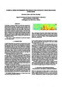
based on double sampling. After selection of a row, the pixel signals after integration of light and after reset are sampled on 2 capacitors. For this purpose, Rs and Ss are closed during a short period (fig. 2). During row readout, the column amplifier multiplexes the stored signals after another on 2 readout busses through exactly the same amplifier. One bus is called the “reset bus” and carries the reset level of each pixel and the other bus is the “signal bus” and carries the light information from each pixel. The Rx and Sx switches take care of the multiplexing. These switches are controlled by the X shift register. The differential signal on both busses carries the image information, free of pixel or column offsets. Since both signals are put on the bus through the same column amplifier, this must happen sequentially. There is thus a delay between the signals on both busses. A sample & hold stage is required on one of the busses in order to synchronize both signals. This takes place in the output amplifier. Unlike in other circuits, there is no need for multiplexing of the reset and signal levels at the double pixel rate. The successive multiplexing of the reset and signal levels is done at the normal pixel rate. While the reset level of one pixel is multiplexed on the ‘reset bus’, the signal level of the next pixel is already been put on the ‘signal bus’ (or vice versa). In our implementation, the sensor has a single-ended output. The synchronization stage is combined with the difference calculation in the output amplifier structure. Figure 3 shows the details of the column multiplexing and output amplifier. On the signal bus, there is a track & hold stage to shift the signal over ½ clock period. The output stage has a black reference clamp circuit. During the first half clock period, the signal of the signal bus is put over the series capacitor. The other side of the capacitor is clamped to the output offset level (or dark reference level). During the second half clock period, the reset signal is put at one side of the capacitor. At the other side, the difference between the reset and signal level appears, free
I. Introduction The problem of fixed pattern noise in active pixel sensors is well known and many circuits have been proposed to correct for it. [1,2] Nevertheless, it is worthwhile to improve the circuits in order to reduce residual FPN to the lowest possible value. This work was initiated by some problems related to radiation effects on CMOS imagers for space use. The strategy to tackle these effects was twofold. First, proper guarding is foreseen for transistor leakage paths that are created by positive charges build up in the oxides. [3] Effects hereof are eliminated by dedicated layout techniques, both for the pixel as well as for the peripheral circuits. Secondly, measures are taken on the circuit level. The analog circuits are designed with a low sensitivity to transistor parameters that are affected by radiation, like the MOSFET threshold voltage. The FPN specification must remain valid also after radiation. This is not always the case. The performance of some classic FPN correction circuits suffers from radiation effects, yielding higher residual FPN values after radiation. Another driving force for this development was the need for higher pixel rates. The fast column multiplexing is the readout speed bottleneck for large devices that have to be read out at high pixel rates. Since many of the current fixed pattern noise reduction circuits need signal multiplexing at the double speed of the readout rate, the maximum readout speed is limited. II. Principle Figure 1 illustrates the principle of the FPN cancellation technique. Like other circuits, it is
1
has potential for deep sub micron technologies with power supply voltages of only 1V. 3) The amplifier can be designed with the desired gain value (e.g. unity gain). E.g. an operational transconductance amplifier (OTA) can be used. A source follower, which is often used in other approaches, has a higher attenuation of the signal and less linearity. 4) The amplifier can be designed so that it can be switched on only when its column is multiplexing a signal on one of the busses. This makes it possible to reduce power consumption. The column amplifier is powered on only when it is used, namely during the readout of the column. 5) The column amplifiers require a simple and straightforward timing (one pulse for ‘R’ and one for ‘S’). The other pulses are generated locally in the columns, from the signals of the pixel clock and the X shift register. 6) No reference voltages are needed for the column amplifiers. 7) Correlated double sampling (with kTC noise elimination) can be done off-chip when the 2 bus signals are both outputted. The R signal is put in a frame buffer. The S signal is subtracted from the prior R signal.
of column or pixel offsets. A track & hold stage makes the output signal stable during the entire clock period. Basically, any kind of amplifying element can be put in the column amplifier. A simple source follower would work, but may result in additional non-linearity and an unwanted voltage level shift. In our implementation, we have used an operational transconductance amplifier, resulting in less signal attenuation and better linearity. III Alternatives Alternatively, only one readout bus can be used on which the reset signal and pixel signal are multiplexed to after each other. The signal on the bus is then very similar to a CCD output signal and can be treated by the same signal processing chain as a CCD camera. The drawback of this approach is that the X multiplexing is at the double speed of the pixel rate. Sub-sampling and windowing is also possible. If this is implemented, an extra register must be foreseen inside each column to memorize the last column that has been read out. While the reset level of a column is read out, the signal level of the memorized column is also multiplexed. Without sub-sampling, each shift register cell can control the 2 adjacent pixels. This is easier to implement. Off-chip correlated double sampling (with kTC noise elimination) can be done when the 2 bus signals are both outputted. The R signal is put in a frame buffer. The S signal is subtracted from the prior R signal
V. Results We have implemented this technique in a radiation tolerant image sensor for space use. Table 1 lists the specifications measured on this device. The remaining local fixed pattern noise (in a window of 10x10 pixels) is 6.1 mV peakto-peak (with a signal saturation level of 1.7 V, i.e. 0.35 %) and 1.2 mV RMS (0.07 %Vsat RMS). The global FPN over the entire array is 0.2% RMS Other specifications are listed in table 1. Total dose radiation tests with Co-60 have been performed up to 10.2 MRad. Even right after radiation (before any annealing step), there is no visible image quality degradation for normal integration times. FPN numbers remain the same. Only a slight increase in dark current could be observed. After 10.2 MRad, the total dose radiation experiment was finished, but the limits of the circuit are far beyond this value. Continued tests are planned to analyze other radiation effects (e.g. protons).
IV. Advantages There are several advantages of this FPN correction approach. Some are already mentioned above. Some others are: 1) The signal path is differential. Electrical crosstalk and power supply variations are common mode effects that influence both the R and S signals in the same way. They will not disturb the output signal. This is especially important for high speed and system-on-a-chip circuits. If desired, a fully differential analog chip output can be produced or the differential output signal of the image sensor can be fed directly to an on-chip processing circuit, like an analog-digital converter. 2) The amplifier in the columns can be designed for low supply voltages. If necessary, a rail-to-rail amplifier can be foreseen. The circuit
Conclusions: A generic concept and circuit for fixed pattern noise correction has been described. The peak-to-peak variation of dark FPN in any 10x10 pixel window is 0.35% of the saturation signal. This is obtained by routing the reset signal and
2
the pixel signal both through the same readout path with the same amplifiers. This concept is still operational for very low power supply levels, which is promising for future deep submicron technologies. This concept has been demonstrated on a 512 x 512 radiation-hard CMOS imager.
Row select
Row reset
Acknowledgement Part of this research has been done as part of the “Optical Inter Satellite Link” programme of the European Space Agency. References [1] S. Mendis, et al, “Progress in CMOS Active Pixel Image Sensors”, Proc. SPIE vol. 2172, pp. 19 (1994) [2] B. Dierickx, et al, “Offset-free offset correction for active pixel sensors”, Proc. 1997 IEEE CCD & AIS workshop, pp. R13 (1997) [3] J. Bogaerts, B.Dierickx, “Total Dose Effects on CMOS Active Pixel Sensors”, proc. SPIE vol. 3965, pp. 157 (2000)
Column amplifier Rs
Rx
Rx R
Ss
Sx
Sx S
Specification Resolution Pixel pitch Technology Total dose radiation tolerance Saturation charge Linear range ( 10 MRad
Signal bus Reset bus
311000 electrons 128500 electrons 5.44 µV/electron 50 mV/s 235 pA/cm2 12 MHz 10 bit 1.7 V 6.1 mV pTp (0.35%) 1.2mV RMS (0.07%) 0.2% RMS 0.63 % 73 electrons
Output amplifier
Fig. 1 : FPN correction technique
Select row Rs Reset row
72.6 dB 35% (500-670 nm) 0.4 200 mW 5V
Ss Row readout
Fig. 2 Timing diagram for Rs and Ss pulses after selection of a new row.
Table 1: image sensor specifications
3
R
Output amplifier
Reset bus
CLK_X
S
CLK_X
Column x+1
R
Column x
S
inv(CLK_X) Signal bus
CLK_X
Shift register Cell x
Shift register Cell x+1
On the falling edge of CLK_X, a new column is selected. Multiplexing of the Ssignal of column x and the R signal of column x-1 starts. On the next falling edge of CLK_X, the output amplifier samples the S-signal of column x. At this moment, also the R-signal of column x starts to be available (on the reset bus). The output signal is generated internally and put at the output after a rising edge on CLK_X.
Black Reference
Single-ended output
Fig.3: X multiplexing scheme for the FPN circuit
Fig. 4 : Image taken right after 10.2 MRad Total Dose radiation (with a Co-60 source, no annealing)
4