JOURNAL OF APPLIED PHYSICS 102, 044305 共2007兲
Formation and characterization of carbon nanowires Amit Kumar, D. K. Avasthi,a兲 and A. Tripathi Materials Science Group, Inter University Accelerator Centre, Post Box 10502, New Delhi-110067, India
L. D. Filip and J. D. Carey Advanced Technology Institute, University of Surrey, Guildford GU2 7XH, United Kingdom
J. C. Pivin CSNSM, Bâtiment 108, 91405 Orsay Campus, France
共Received 11 June 2007; accepted 17 June 2007; published online 21 August 2007兲 This article reports on the formation and electronic characteristics of conducting carbon nanowires produced by swift heavy ion irradiation of a fullerene thin film. This study shows that it is possible to create arrays of carbon nanowires, which are perfectly parallel to each other and perpendicular to the substrate. As-deposited fullerene films exhibit poor field emission characteristics with breakdown fields as high as 51 V / m, whereas low dose ion irradiated fullerene film produces a threshold field as low as 9 V / m. The present approach of making conducting carbon nanowires by ion irradiation for potential field emitters and large area applications is also discussed. © 2007 American Institute of Physics. 关DOI: 10.1063/1.2767227兴 I. INTRODUCTION
One of the main goals of nanotechnology is the ability to control or engineer the structure and properties of materials on the nanometer scale and to take advantage of the inherent properties, such as enhanced reactivity or quantum confinement. The construction of nanoelectronic devices is technologically challenging and many different approaches are possible. The controlled growth of a single nanowire or an ensemble of nanowires, their growth direction, suitable alignment, and spacing on a substrate is of paramount importance and critical to the realization of integrated electronic and photonic devices. Many methods have been developed for the fabrication of nanowire arrays including template methods,1,2 catalytic growth,3 Langmuir Blodgett, and electrospinning.4 Ion beam methods are now emerging as a tool in nanofabrication for structuring material on the nanometer scale.5,6 It is known that when a swift heavy ion 共SHI兲 i.e., a heavy ion with energy ⬎1 MeV/ nucleon, passes through a material, it induces a continuous trail of damage with several nanometers width and typically several tens of microns in length. Such ion tracks consist of material with properties that are drastically changed when compared with the surrounding virgin material. As a consequence this is a way to nanostructure a material and to change the local electronic and structural properties on the nanometer scale. In this article we report on the use of SHI to produce arrays of carbon nanowires and characterize the conduction and field emission properties. There has been considerable interest in field emission from nanostructured carbon-based system such as diamond, diamond-like carbon, carbon nanotubes, fullerene, and nanostructured carbon for field emission devices.7,8 Emission from carbon-based materials depends on various parameters, a兲
Author to whom correspondence should be addressed; electronic mail:
[email protected]
0021-8979/2007/102共4兲/044305/4/$23.00
such as negative electron affinity, band gap, surface termination, sp2 and sp3 content, etc., and is often reported as being localized rather than uniform.9–11 In the case of carbon nanotubes and nanowires the effects of varying the aspect ratio and the proximity screening12 need also to be taken into account. Ion irradiation of fullerene thin films 关Fig. 1共a兲兴 is known to break the fullerene cages and within the nanosized track to form nanocrystalline graphite.13,14 From a technological viewpoint, one of the more important aspects is the development of large scale and controllable production methods, especially for aligned nanowire production. Although electron beam lithography15 allows the formation of catalyst sites for aligned growth of nanowires, this serial technique is too slow for scalable mass production. Ion implantation is a well established method for transistor technology and offers the possibility of large area production of emitters. This has prompted us to synthesize carbon nanowire field emitters by ion irradiation. II. EXPERIMENT
Fullerene thin films of 500 nm thickness were deposited on 50 nm thick Au layers on a Si substrate. The need for a Au layer was to facilitate the characterization of conducting channels by conducting atomic force microscope 共C-AFM兲 as shown in Fig. 1共b兲. The gold films were deposited on Si substrate by resistive heating and the fullerene films were deposited on these Au films by sublimation of a C60 pellet. A small area of the Au film was masked so that it can be used as a contact for conducting AFM. The evaporation was performed at pressure of 5 ⫻ 10−7 mbar, achieved by using a diffusion pump with a LN2 trap. The thickness of the film was monitored by a quartz crystal thickness monitor. The fullerene films were irradiated by 120 MeV Au ions at fluence of 5 ⫻ 109 ions/ cm2 using 15⫻ 106 V Pelletron accelerator at Inter-University Accelerator Centre, New Delhi, India. The Au ion beam deposits ⬃13 keV/ nm by electronic
102, 044305-1
© 2007 American Institute of Physics
Downloaded 31 Mar 2009 to 131.227.178.132. Redistribution subject to AIP license or copyright; see http://jap.aip.org/jap/copyright.jsp
044305-2
Kumar et al.
J. Appl. Phys. 102, 044305 共2007兲
FIG. 2. 共Color online兲 Conducting AFM image, of the irradiated fullerene thin film. The vertical rods represent the current flowing through the conducting nanowires.
III. RESULTS AND DISCUSSION
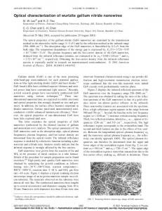
FIG. 1. 共Color online兲 Schematic of the 共a兲 conducting carbon nanowires formation in fullerene films by energetic ion irradiation and 共b兲 conducting atomic force microscopy measurement of carbon nanowires.
energy loss 共due to inelastic collision兲 and ⬃102.4 eV/ nm by nuclear energy loss 共due to elastic collision兲 as estimated by Monte-Carlo simulation 共SRIM兲.16 From the Monte Carlo simulations, the electronic energy loss in the entire thickness of the film is uniform and ions get buried deep 共23 m兲 inside the Si substrate. The fluences were kept low so as to minimize the overlap of the ion tracks. The vacuum during irradiation was approximately 10−6 mbar and the current was about 0.5 pnA 共1 particle nA= 6.25⫻ 109 ions/ s兲. The ion beam was scanned in area of 1 cm2 by an electromagnetic scanner. The C-AFM measurements were performed on the pristine and irradiated samples using the Digital Instrument Nanoscope III. The field emission characteristics of pristine and irradiated films were examined using a sphere-to-plane geometry in which a 5 mm stainless-steel ball bearing is suspended above the surface at a high positive potential in a vacuum better than 4 ⫻ 10−6 mbar.17 Field emission measurements are made by varying the relative separation between the probe and sample using a high precision manipulator with a known step size. A threshold voltage corresponding to an emission current of 1 nA is calculated at each position. A plot of the variation of the threshold voltage against relative probe separation 共not shown here兲 provides the threshold field.
Figure 2 shows the conducting AFM scan of a film irradiated with 120 MeV Au ions at a fluence of 5 ⫻ 109 ions/ cm2. The image shows that the current in the ion tracks is significantly higher than in regions not hit by the ions. For a fluence of 5 ⫻ 109 ions cm−2, a simple area estimate suggests that there should be 50 tracks per square micron or seven tracks per micron. A current of approximately 10 nA was measured 共for 4 V兲 in a cylindrical region with a diameter of a few tens of nanometers, corresponding to an ion impact. The sectional analysis reveals that the diameter of the semiconducting zone varies from 20 nm 共single or few impacts兲 to 100 nm 共many impacts兲. The observed tracks show some mismatching to incident ions. Mismatch between fluence and the ion track areal density may result from random ion impacts resulting in overlapping tracks and/or lateral conduction with the neighboring tracks. As a result not all of the nanowires are perpendicular to the substrate. In addition the finite size of tip may have influence. Fourier transform infrared spectroscopy18 has previously revealed that the track is surrounded by a polymerized annular cylindrical region. The carbon nanowires are predominantly parallel to each other and perpendicular to the substrate, because the irradiation has been performed perfectly perpendicular to fullerene films. The length of the CNW can be tuned by the thickness of fullerene film and its orientation can be engineered by simply changing the incidence angle of the ion beam. No catalysts are required and only a few seconds are required for nanowire growth. This is one of the advantages of the ion beam approach. The other interest of using swift heavy ion irradiation with respect to chemical routes to fabricate emission tips attached to a substrate is that all the tips are perfectly parallel to each other, their areal density and separation to height ratio can be controlled simply by the ion fluence and film thickness. Therefore, we can say that the present technique has definite advantages over the other techniques. Nowadays some accelerator facilities are commercially used for the applications, which require low flu-
Downloaded 31 Mar 2009 to 131.227.178.132. Redistribution subject to AIP license or copyright; see http://jap.aip.org/jap/copyright.jsp
044305-3
Kumar et al.
J. Appl. Phys. 102, 044305 共2007兲
FIG. 3. The current versus voltage 共I − V兲 characteristics of the nanowire as measured in conducting atomic force microscopy.
ence and therefore small irradiation time. The creation of micro filters/ micropores by etching of the low fluence irradiated polymers, is one such example. The I − V measurements on ion hit regions 关carbon nanowire 共CNW兲兴 in the irradiated film at fluence of 5 ⫻ 109 ions/ cm2 is shown in Fig. 3. The vertical alignment and effective high aspect ratio of CNWs makes them attractive from a field emission perspective. The field emission properties have been studied on the synthesized CNWs as shown in Fig. 4共a兲. A threshold field of about 9 V / m has been observed for CNWs where as the pristine films shown breakdown behavior at 51 V / m. The current–voltage characteristics repeated for four times are presented with no significant difference between them, which indicates good stability. The field emission properties of pristine film are shown in the inset of Fig. 4共a兲. The Fowler– Nordheim representation of one of the field emission characteristics of the irradiated sample is shown in Fig. 4共b兲. The apparent linear fit allows estimate to the field enhancement factor, . Assuming that the work function of the nanowires is approximately 5 eV, a value of  = 429 is estimated. At a typical threshold applied field of 9 V / m, the average local electric field is 3.8 V/nm, which is comparable to emission from carbon nanotubes.19 Lower values of applied field, corresponding to higher enhancement factors, are sometimes reported from ideal aligned nanowires and nanotubes.12,19 However, at high areal densities inter nanowire proximity screening becomes a significant factor. In a similar work by Nilsson et al.,12 they estimated that the ideal average separation between nanowires should be about twice the length of nanowire. With typical nanowire lengths of 500 nm 共corresponding to the film thickness兲, the average separation between impacts sites at this fluence is approximately 710 nm as estimated by section analysis. In such a situation, proximity screening is likely to be occurring to some extent. It should also be noted that in the study by Schwen et al.,20 larger threshold applied fields of 30 V / m were reported for 350 MeV Au ion SHI into tetrahedral amorphous carbon 共a-C兲 grown by mass selected ion beam deposition. They attributed the high threshold field solely to the embedding of the nanowires in the a-C matrix whose dielectric constant
FIG. 4. 共Color online兲 共a兲. The emission current versus applied voltage of the synthesized carbon nanowires by ion irradiation. Four curves are shown to demonstrate the reproducibility of emission. 共Inset兲 Emission from an unimplanted fullerene film. The inset shows the emission properties of pristine film. 共b兲 The Fowler–Nordheim representation of one of the curves in 共a兲 of the synthesized carbon nanowires by ion irradiation.
reduces the field experienced by the nanowire and consequentially larger applied fields are required for emission. However, in their study the mean separation between ion tracts was reported to be 80 nm and the length of the nanowires to be no larger than 200 nm. In such a situation the nanowires will be very strongly electrostatic screened by other nanowires as the separation-to-length ratio is only 0.4. In our study the nanowires are separated by, on average, 710 nm and have an average length of 500 nm 共corresponding to the film thickness兲. The higher average internanowire separation to length ratio in this study 共1.4兲 suggests the presence of less proximity screening and helps us to explain the lower applied field required for emission when compared with the study by Schwen and colleagues.20 The field enhancement factor value of the synthesized carbon nanowires in fullerene matrix is comparable to carbon nanohorn prepared by laser ablation of graphite, chemical vapor deposition grown carbon nanofibers and multi walled carbon nantubes.19,21 The improved field emission arises due to the structural transformation along the ion paths. Some of us have shown previ-
Downloaded 31 Mar 2009 to 131.227.178.132. Redistribution subject to AIP license or copyright; see http://jap.aip.org/jap/copyright.jsp
044305-4
J. Appl. Phys. 102, 044305 共2007兲
Kumar et al.
ously that the conductivity of the SHI irradiated fullerene thin film increases significantly,12,22 which is attributed to the fact that the swift heavy ions create track in fullerene thin film, breaking the fullerene cages within the track to form nanocrystalline graphite embedded in a-C carbon,14 which is electrically more conducting than the parent fullerene molecule. IV. CONCLUSION
In summary, the fabrication of conducting carbon nanowires in fullerene matrix by heavy ion irradiation is reported and their electrical and field emission properties are studied. No catalyst or any further purification is required, unlike in the case of carbon nanotubes. Irradiation using the mask of desired geometry can create according geometry nanowires and the conductive AFM measurements show that the nanowires are parallel to each other and perpendicular to substrate. Irradiation only requires a short time, which allows for synthesis in large quantities. Thus, the present approach of making carbon nanowires is quite promising and these CNWs may be useful for better field emitters and large scale applications. ACKNOWLEDGMENTS
Two of the authors 共D.K.A. and J.C.P.兲 are thankful to the Indo French Centre for Promotion of Advanced Research for financial support to carry out work on “Generation of nanophase by energetic ion beams”. One of the authors 共A.K.兲 is thankful to Council of Scientific and Industrial Research 共CSIR兲, New Delhi, India for providing fellowship. They are also thankful to DST for providing the financial support to procure AFM/C-AFM under the IRPHA project. Work at Surrey is sponsored by the EPSRC.
S. J. Limmer and G. Z. Cao, Adv. Mater. 15, 427 共2003兲. N. A. Melosh, A. Boukai, F. Diana, B. Gerardot, A. Badolato, P. M. Petroff, and J. R. Heath, Science 300, 112 共2003兲. 3 Z. F. Ren, Z. P. Huang, J. W. Xu, J. H. Wang, P. Bush, M. P. Siegal, and P. N. Provencio, Science 282, 1105 共1998兲. 4 X. D. Wang, C. J. Summers, and Z. L. Wang, Nano Lett. 4, 423 共2004兲. 5 S. Seki, K. Maeda, S. Tagawa, H. Kudoh, M. Sugimoio, Y. Morita, and H. Shibata, Adv. Mater. 13, 1663 共2001兲. 6 S. K. Srivastava, D. K. Avasthi, and E. Pipple, Nanotechnology 17, 2518 共2006兲. 7 M. W. Geis, J. C. Twichell, J. Macaulay, and K. Okano, Appl. Phys. Lett. 67, 1328 共1995兲. 8 R. C. Smith, J. D. Carey, R. J. Murphy, W. J. Blau, J. N. Coleman, and S. R. P. Silva, Appl. Phys. Lett. 87, 263105 共2005兲. 9 T. Hara, J. Onoe, and K. Takeuchi, J. Appl. Phys. 92, 7302 共2002兲. 10 J. D. Carey, R. D. Forrest, R. U. A. Khan, and S. R. P. Silva, Appl. Phys. Lett. 77, 2006 共2000兲. 11 W. Zhu, G. P. Kochanski, and S. Jin, Science 282, 1471 共1998兲. 12 L. Nilsson, O. Groening, C. Emmenegger, O. Kuettel, E. Schaller, L. Schlapbach, H. Kind, J.-M. Bonard, and K. Kern, Appl. Phys. Lett. 76, 2071 共2000兲. 13 J. Kastner, H. Kuzmany, and L. Palmetshofer, Appl. Phys. Lett. 65, 543 共1994兲. 14 N. Bajwa, A. Ingale, D. K. Avasthi, R. Kumar, K. Dharamvir, and V. K. Jindal, J. Appl. Phys. 94, 326 共2003兲. 15 K. B. K. Teo et al., Nanotechnology 14, 204 共2003兲. 16 J. F. Zeigler, J. P. Biersack, and V. Littmark, The Stopping and Range of Ions in Solids 共Pergamon, New York, 1985兲. 17 J. D. Carey, R. D. Forrest, and S. R. P. Silva, Appl. Phys. Lett. 78, 2339 共2001兲. 18 A. Kumar, D. K. Avasthi, A. Tripathi, D. Kabiraj, F. Singh, and J. C. Pivin, J. Appl. Phys. 101, 014308 共2007兲. 19 J.-M. Bonard, R. Gaal, S. Garaj, L. Thien-Nga, L. Forro, K. Takahashi, F. Kokai, M. Yudasaka, and S. Iijima, J. Appl. Phys. 91, 10107 共2002兲. 20 D. Schwen, C. Ronning, and H. Hofsass, Diamond Relat. Mater. 13, 1032 共2004兲; N. Koenigsfeld, H. Hofsass, and D. Schwen, ibid. 12, 469 共2003兲. 21 J.-M. Bonard, N. Weiss, H. Kind, T. Stockli, L. Forro, K. Kern, and A. Chatelain, Adv. Mater. 13, 184 共2001兲. 22 A. Kumar, F. Singh, R. Kumar, J. C. Pivin, and D. K. Avasthi, Solid State Commun. 138, 448 共2006兲. 1 2
Downloaded 31 Mar 2009 to 131.227.178.132. Redistribution subject to AIP license or copyright; see http://jap.aip.org/jap/copyright.jsp