ISSCC 2006 / SESSION 2 / BIOMEDICAL SYSTEMS / 2.2. 2.2. Fully Electronic CMOS DNA Detection Array Based on Capacitance Measurement with On-Chip.
ISSCC 2006 / SESSION 2 / BIOMEDICAL SYSTEMS / 2.2
2.2
Fully Electronic CMOS DNA Detection Array Based on Capacitance Measurement with On-Chip Analog-to-Digital Conversion
Claudio Stagni Degli Esposti1, Carlotta Guiducci1, Christian Paulus2, Meinrad Schienle2, Marcin Augustyniak3, Giampaolo Zuccheri1, Bruno Samorì1, Luca Benini1, Bruno Riccó1, Roland Thewes3 1
University of Bologna, Bologna, Italy Siemens, Munich, Germany 3 Infineon Technologies, Munich, Germany 2
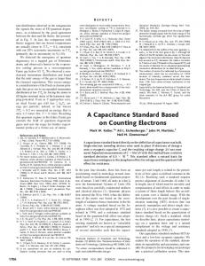
Protein and DNA microarray chips enable the highly parallel investigation concerning the presence and amount of specific proteins or DNA sequences within a given sample. For this purpose, known probe molecules are immobilized on the chip surface, and binding events with matching target molecules from the sample are detected. Today, optical detection techniques are widespread (Fig. 2.2.1, top). There, the target molecules are labeled with fluorescence markers. After the binding and a subsequent washing phase the chip is illuminated, and a fluorescence light image of the array reveals the positions with matching (i.e. chemically bound) probe and target molecules [1]. In Fig. 2.2.1 (bottom), a fully electronic, label-free method is schematically depicted which circumvents expensive optical setups and lowers the biochemical complexity by avoiding the labeling step. The equivalent electrical impedance (modeled by Rsens , Csens) is dominated by the reactive component Csens, because Rsens is very large (due to the quasi-ideal insulating properties of the electrode-solution interface [2]). Chemical binding events close to the surface of the sensor array electrodes lead to a sizable decrease of Csens [3]. In this work, we present a 16×8 CMOS sensor array for detecting DNA hybridization based on capacitance measurements. A single sensor consists of two interdigitated gold electrodes. The electrode width and spacing are 1µm, the total sensor diameter is 200µm, and the sensor pitch is 300µm. Chips with a total area of 25mm2 are fabricated in a 0.5µm, 5V standard CMOS process extended with extra steps to process the noble metal [5]. A chip micrograph with a blow-up of a single sensor is shown in Fig. 2.2.7. Figure 2.2.2 shows the capacitance measurement principle of the circuit underneath each sensor site. A constant current source (Iref) is used to alternately charge / discharge the two terminals of the sensor. The voltage difference between the two terminals is monitored using a fully differential comparator. When this amplitude exceeds a defined threshold (Vref), all switches change their state so that the charged (discharged) sensor terminal is discharged (charged) again, and the threshold voltage changes polarity. As a consequence, approximately triangular voltage waveforms are obtained at the sensor terminals VA and VB. The resulting frequency f of positive threshold crossings is measured by counting Vout pulses. The resulting frequency f as a function of current and amplitude is given by f = { Csens × Rsens × ln [ 1 / (1- Vref / ( Iref × Rsens ) ] }-1 For not too low frequencies (i.e. not too low values of Iref) the contribution of Rsens is negligible and after some mathematics the approximation Csens = Iref / ( 2 Vref f ) is obtained for the interface capacitance. The frequency range used here is 500Hz to 1kHz.
Figure 2.2.3 shows circuit design details. The sensor current Iref is provided by cascaded n- and p-MOS current sources. The pMOS source is part of an in-sensor site p-MOS current mirror biased by an n-MOS current source. The n-MOS current sources bias voltages are generated by an n-MOS cascaded current mirror input stage located at the periphery of the array. A fully-differential amplifier is operated as a comparator, whose number of output pulses within an externally settable time interval is counted by an in-sensor-site 22-stage counter [6], so that fully digital signals are available at the output of the sensor site circuit. Sensing circuit characterization results are exemplified in Fig. 2.2.4, which shows measured frequencies of the approximately triangular voltage waveform as a function of Iref for four test circuits. Solid lines correspond to pure single capacitances, 1nF and 4.7nF, respectively, dotted lines to capacitances in parallel with ohmic resistances, 1nF with 200kΩ and 4.7nF with 200kΩ, respectively. Two-terminal sensors on the chip have capacitance values of similar magnitude as compared to these test capacitances. The plot shows that the integrated sensors are able to measure reliably capacitances in this range, even in the presence of a non-negligible parallel resistance Rsens (which may be smaller than expected under unfavourable experimental conditions, due to non-ideal conditions of the molecular layer). Inter-site and inter-chip variations are extremely small (standard deviation = 0.3% within a set of 20 test chips). Characterization of the chip operated as a DNA sensor is detailed next. Figure 2.2.5 shows the average capacitance variation with respect to bare gold electrodes of: (i) electrodes functionalized with 30-mer probes; (ii) functionalized electrodes with specifically bound complementary 25-mer DNA strands; (iii) functionalized electrodes exposed to non-complementary DNA strands. We observe that, on average, functionalization leads to a decrease in capacitance, and that specific DNA binding leads to a further decrease that is significantly larger than that due to non-specific binding. Satisfactory multiple-electrode DNA-recognition on a single array is demonstrated in Fig. 2.2.6. There, the relative variation of capacitance is depicted of 12 functionalized electrodes before and after hybridization with complementary DNA samples. The horizontal line shows the worst-case (over more than 50 measurements) electrode capacitance variation due to non-specific binding. The variation due to hybridization is clearly distinguishable from the worst-case due to non-specific binding, even if we consider the error bars obtained by repeating several times electrical measurements and rinsing cycles. References: [1] M. Schena ed., “DNA Microarrays: A Practical Approach,” Oxford University Press, p. 209, Oxford, UK, 2000. [2] V. Mirsky et al., “Capacitive Monitoring of Protein Immobilization and Antigen-Antibody Reactions on Monomolecular Alkylthiol Films on Gold Electrodes,” Biosensors and Bioelectronics, p. 977-989, Jan., 1997. [3] C. Guiducci et al., “DNA Detection by Integrable Electronics,” Biosensors and Bioelectronics, p. 781-787, Mar., 2004. [4] C. Berggren et al., “A Feasibility Study of S Capacitive Biosensor for Direct Detection of DNA Hybridization,” Electroanalysis, p. 156-160, May, 1999. [5] F. Hofmann et al., “Fully Electronic DNA Detection on a CMOS Chip: Device and Process Issues,” Tech. Dig. IEDM, p. 488-491, Dec., 2002 [6] M. Schienle et al., “A Fully Electronic DNA Sensor with 128 Positions and In-Pixel A/D Conversion,” ISSCC Dig. Tech. Papers, pp. 220-221, Feb., 2004.
• 2006 IEEE International Solid-State Circuits Conference
1-4244-0079-1/06 ©2006 IEEE
ISSCC 2006 / February 6, 2006 / 2:00 PM
VA Vout Iref Vref VB
Biological layers
Electrical behavior
VA-VB=Vref
Rsense Csense
Protein
VA-VB= -Vref VA VB
Vref t
Vout
Alkanthiol or DNA
T
Figure 2.2.1: Schematic description of fluorescence label based operation of micro-arrays and impedance-based label-free fully electronic detection method.
Iref
Vcasc Vbias
VA
t
Figure 2.2.2: Detection circuit principle.
22 bit counter & shift register
digital out
Vbias
VB
control
Vref
Figure 2.2.3: Diagram of sensor site circuit.
Figure 2.2.4: Measured frequency versus bias current for different test impedances.
Figure 2.2.5: Capacitance variation (on average) with respect to gold after surface bio-modification.
Figure 2.2.6: Multiple sites measurements of DNA hybridization.A reference horizontal line has been added to compare results of hybridized electrodes with the worst-case variation due to non-specific binding.
DIGEST OF TECHNICAL PAPERS •
ISSCC 2006 / SESSION 2 / BIOMEDICAL SYSTEMS / 2.2
X-Y DECODERS
Digital and Analog I/O Pads
128 pixels Array Figure 2.2.7: Chip micrograph. The inset shows a single sensor.
• 2006 IEEE International Solid-State Circuits Conference
1-4244-0079-1/06 ©2006 IEEE
ISSCC 2006 / SESSION 2 / BIOMEDICAL SYSTEMS / 2.2
Biological layers
Electrical behavior Rsense
Protein
Csense
Alkanthiol or DNA Figure 2.2.1: Schematic description of fluorescence label based operation of micro-arrays and impedance-based label-free fully electronic detection method.
• 2006 IEEE International Solid-State Circuits Conference
1-4244-0079-1/06 ©2006 IEEE
ISSCC 2006 / SESSION 2 / BIOMEDICAL SYSTEMS / 2.2
VA Vout Iref Vref VB VA-VB=Vref
VA-VB= -Vref VA VB
Vref t
Vout T
t
Figure 2.2.2: Detection circuit principle.
• 2006 IEEE International Solid-State Circuits Conference
1-4244-0079-1/06 ©2006 IEEE
ISSCC 2006 / SESSION 2 / BIOMEDICAL SYSTEMS / 2.2
Iref
Vcasc Vbias
VA
22 bit counter & shift register
digital out
Vbias
VB
control
Vref Figure 2.2.3: Diagram of sensor site circuit.
• 2006 IEEE International Solid-State Circuits Conference
1-4244-0079-1/06 ©2006 IEEE
ISSCC 2006 / SESSION 2 / BIOMEDICAL SYSTEMS / 2.2
Figure 2.2.4: Measured frequency versus bias current for different test impedances.
• 2006 IEEE International Solid-State Circuits Conference
1-4244-0079-1/06 ©2006 IEEE
ISSCC 2006 / SESSION 2 / BIOMEDICAL SYSTEMS / 2.2
Figure 2.2.5: Capacitance variation (on average) with respect to gold after surface bio-modification.
• 2006 IEEE International Solid-State Circuits Conference
1-4244-0079-1/06 ©2006 IEEE
ISSCC 2006 / SESSION 2 / BIOMEDICAL SYSTEMS / 2.2
Figure 2.2.6: Multiple sites measurements of DNA hybridization.A reference horizontal line has been added to compare results of hybridized electrodes with the worst-case variation due to non-specific binding.
• 2006 IEEE International Solid-State Circuits Conference
1-4244-0079-1/06 ©2006 IEEE
ISSCC 2006 / SESSION 2 / BIOMEDICAL SYSTEMS / 2.2
X-Y DECODERS
Digital and Analog I/O Pads
128 pixels Array Figure 2.2.7: Chip micrograph. The inset shows a single sensor.
• 2006 IEEE International Solid-State Circuits Conference
1-4244-0079-1/06 ©2006 IEEE